

Page 1
STB70NF02L
N-CHANNEL 20V - 0.006
LOW GATE CHARGE STripFET POWER MOSFET
TYPE V
ST B70NF02L 20 V < 0.009 Ω 70 A
■ TYPICALR
■ TYPICALQ
■ OPTIMAL R
■ CONDUCTION LOSSESREDUCED
■ SWITCHINGLOSSESREDUCED
DS(on)
g
DSS
= 0.006 Ω
= 36 nC @ 10V
DS(on)xQg
DESCRIPTION
This applicationspecific Power Mosfet is the third
generation of STMicroelectronics unique ”Single
Feature Size” strip-based process. The resulting transistor shows the best trade-off between
on-resistance and gate charge. When used as
high and low side in buck regulators, it gives the
best performancein termsof both conductionand
switching losses. This is extremely important for
motherboardswhere fast switching and high efficiencyare of paramount importance.
R
DS(on)
TRADE-OFF
I
D
Ω
- 70A D2PAK
PRELIMINARY DATA
3
1
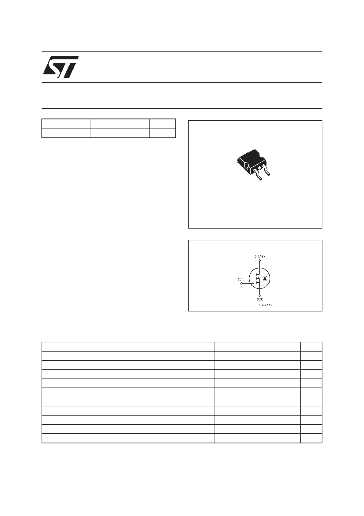
D2PAK
TO-263
ADD SUFFIX ”T4” FOR ORDERING IN TAPE & REEL
INTERNAL SCHEMATIC DIAGRAM
APPLICATIONS
■ SPECIFICALLYDESIGNEDAND
OPTIMISEDFOR HIGH EFFICIENCY CPU
CORE DC/DC CONVERTERS
ABSOLUTE MAXIMUM RATINGS
Symbol Parameter Value Unit
V
V
V
I
DM
P
T
(•) Pulse width limited by safeoperating area
Dra in- sour c e Volt age ( VGS=0) 20 V
DS
Dra in- gate V ol t age ( RGS=20kΩ)20V
DGR
Gat e-source Voltage
GS
I
Dra in C u rr ent (c ontinuous) at Tc=25oC70A
D
I
Dra in C u rr ent (c ontinuous) at Tc=100oC50A
D
(•) Dra in Current ( p uls ed ) 280 A
Tot al Dis s ipation at Tc=25oC 100 W
tot
Der ati ng Fac t or 0.67 W/
St orage Tempe rat ure -65 t o 175
stg
T
Max. O perating Junc t ion T emperat ure 175
j
20 V
±
o
C
o
C
o
C
20/01/2000
1/6
Page 2
STB70NF02L
THERMAL DATA
R
thj-case
R
thj-amb
T
Ther mal Resistanc e Junct ion-case Max
Ther mal Resistanc e Junct ion-ambient Max
Maximum Lead Tem pe ra tur e For Solder ing Purpose
l
1.5
62.5
300
o
C/W
o
C/W
o
C
ELECTRICAL CHARACTERISTICS
=25oC unless otherwisespecified)
(T
case
OFF
Symbol Parameter Test Conditions Min. Typ. Max. Unit
V
(BR)DSS
Drain-source
ID=250µAVGS=0 20 V
Break dow n V o lt age
I
DSS
I
GSS
Zero Gate Voltage
Drain Cur re nt ( V
GS
Gat e- bod y L eakage
Current (V
DS
=0)
=0)
V
=MaxRating
DS
=MaxRating Tc=125oC
V
DS
V
= ± 20 V ± 100 nA
GS
1
10
ON(∗)
Symbol Parameter Test Conditions Min. Typ. Max. Unit
V
GS(th)
R
DS(on)
I
D(on)
Gate Threshold Volt age VDS=VGSID= 250 µA12.5V
Sta t ic Drain -s ource On
Resistance
On State Drain Current VDS>I
VGS=10V ID=35A
V
=5V ID=18A
GS
D(on)xRDS(on )max
0.006
0.011
0.009
0.015
70 A
VGS=10V
DYNAMIC
Symbol Parameter Test Conditions Min. Typ. Max. Unit
g
(∗)Forward
fs
Tr ansc on duc tance
C
C
C
Input Capac i t ance
iss
Out put Capacitance
oss
Reverse Tr ansfer
rss
Capacit a nc e
VDS>I
D(on)xRDS(on )maxID
=35 A 40 S
VDS=25V f=1MHz VGS= 0 1500
900
200
µA
µ
Ω
Ω
pF
pF
pF
A
2/6
Page 3

STB70NF02L
ELECTRICAL CHARACTERISTICS
(continued)
SWITCHING ON
Symbol Parameter Test Conditions Min. Typ. Max. Unit
t
d(on)
t
Tur n-on Delay Time
Rise Ti me
r
VDD=10V ID=35A
R
=4.7
G
Ω
VGS=4.5V
25
480
(Resis t iv e Loa d, s ee fig. 3)
Q
Q
Q
Tot al Gat e Charge
g
Gat e- Source Charge
gs
Gate-Drain Charge
gd
VDD=16V ID=46A VGS=10V 36
5
10
45 nC
SWITCHING OFF
Symbol Parameter Test Conditions Min. Typ. Max. Unit
t
d(off)
Tur n-of f Delay Time
t
Fall T ime
f
VDD=10V ID=35A
R
=4.7
G
Ω
VGS=4.5V
30
110
(Resis t iv e Loa d, s ee fig. 3)
SOURCEDRAINDIODE
Symbol Parameter Test Conditions Min. Typ. Max. Unit
I
SD
I
SDM
V
SD
t
Q
I
RRM
(∗) Pulsed:Pulse duration = 300µs, duty cycle 1.5%
(•) Pulse width limited by safe operating area
Source-drain Current
(•)
Source-drain Current
70
280
(pulsed)
(∗)ForwardOnVoltage ISD=70 A VGS=0 1.2 V
Reverse Recovery
rr
Time
Reverse Recovery
rr
ISD= 70 A di/dt = 100 A /µs
=15V Tj=150oC
V
DD
(see test circuit, fig. 5)
60
100
Charge
Reverse Recovery
2
Current
ns
ns
nC
nC
ns
ns
A
A
ns
nC
A
3/6
Page 4

STB70NF02L
Fig. 1:
UnclampedInductiveLoad TestCircuit
Fig. 3: SwitchingTimes Test Circuits For
ResistiveLoad
Fig. 2:
UnclampedInductiveWaveform
Fig. 4: Gate Chargetest Circuit
Fig. 5:
Test CircuitFor InductiveLoad Switching
And Diode Recovery Times
4/6
Page 5

TO-263 (D2PAK) MECHANICAL DATA
STB70NF02L
DIM.
MIN. TYP. MAX. MIN. TYP. MAX.
A 4.4 4.6 0.173 0.181
A1 2.49 2.69 0.098 0.106
B 0.7 0.93 0.027 0.036
B2 1.14 1.7 0.044 0.067
C 0.45 0.6 0.017 0.023
C2 1.21 1.36 0.047 0.053
D 8.95 9.35 0.352 0.368
E 10 10.4 0.393 0.409
G 4.88 5.28 0.192 0.208
L 15 15.85 0.590 0.624
L2 1.27 1.4 0.050 0.055
L3 1.4 1.75 0.055 0.068
mm inch
D
A
C2
DETAIL”A”
C
A2
DETAIL”A”
A1
B2
E
L2
L
L3
B
G
P011P6/E
5/6
Page 6

STB70NF02L
Information furnishedis believed to be accurateand reliable.However, STMicroelectronics assumes no responsibilityfor the consequences
of use of such information nor for any infringement of patents or other rights of third parties which may resultfrom its use. No licenseis
granted by implication or otherwise under any patent or patentrights of STMicroelectronics. Specificationmentioned in this publicationare
subjecttochange withoutnotice.Thispublication supersedes andreplaces all informationpreviously supplied.STMicroelectronicsproducts
are not authorized for use as critical components in lifesupportdevices or systems without express written approval of STMicroelectronics.
The STlogo is a trademark of STMicroelectronics
1999 STMicroelectronics – Printed in Italy – All Rights Reserved
STMicroelectronics GROUP OF COMPANIES
Australia - Brazil - China - Finland - France - Germany - Hong Kong - India - Italy - Japan - Malaysia - Malta - Morocco -
6/6
Singapore - Spain - Sweden - Switzerland - United Kingdom - U.S.A.
http://www.st.com
.
 Loading...