

Page 1
• SUPPLY VOLTAGE 2.8V
S
• LOW CURRENT CONSUMPTION
• VERY LOW NOISE FIGURE:
NF=1.5dB @ 950MHz
NF=1.9dB @ 1850MHz
NF=2dB @ 1950MHz
• DIGITAL GAIN CONTROL
APPLICATIONS
TRI-BAND GSM/DCS/PCS FRONT-ENDS
STB7003
TRI-BAND GSM/DCS/PCS LNA
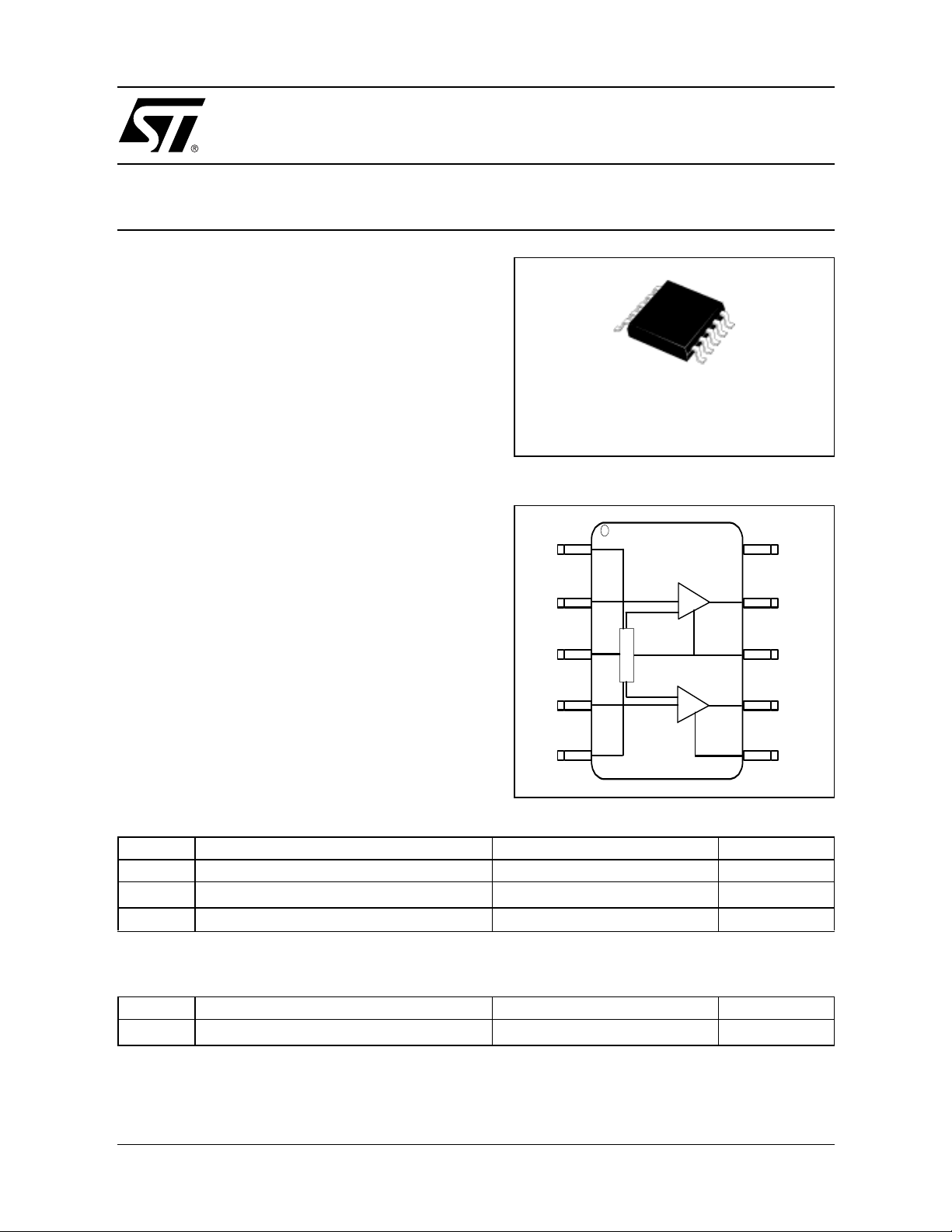
MSOP10-EP
(exposed pad)
ORDER CODE
STB7003
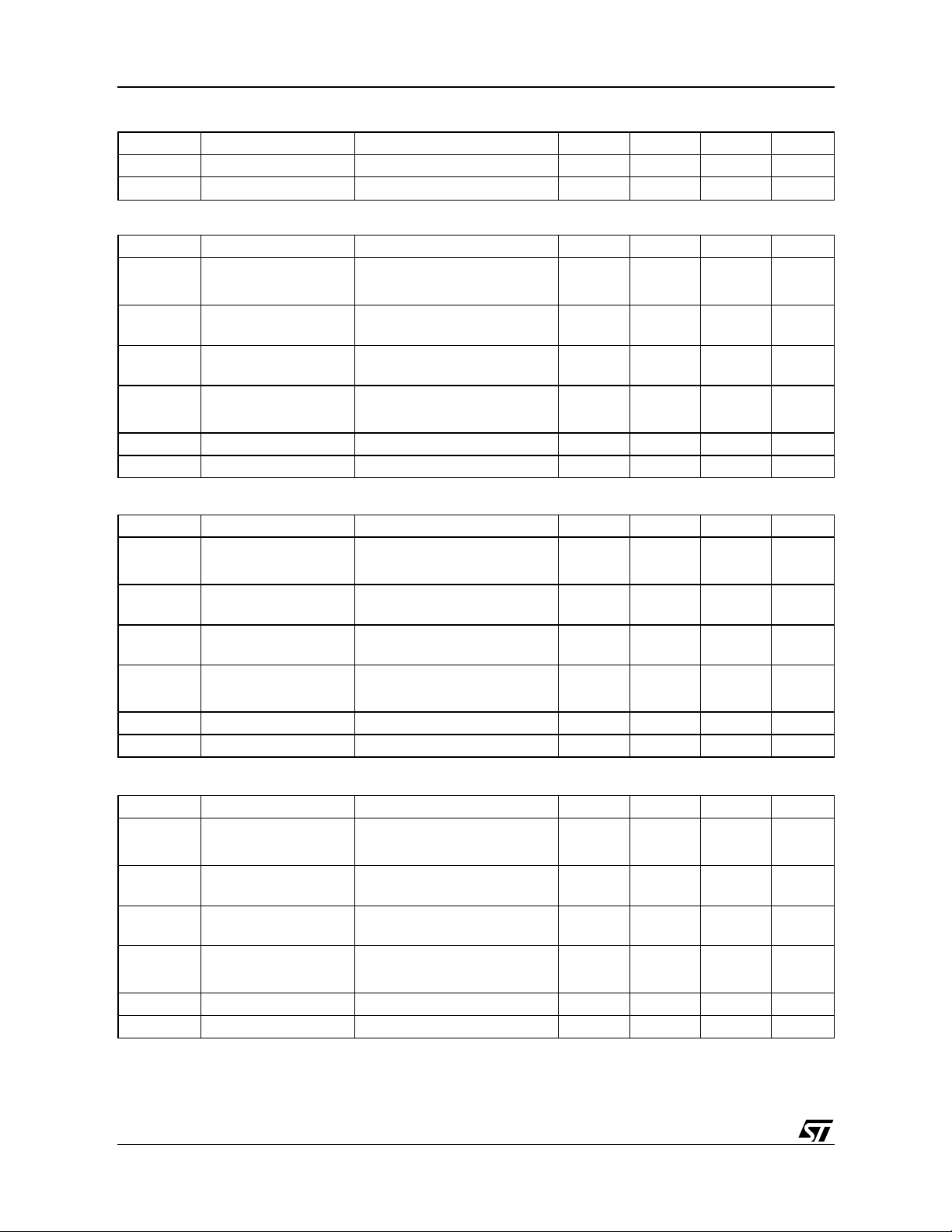
FUNCTIONAL BLOCK DIAGRAM
BRANDING
7003
DESCRIPTION
PD
The STB7003 is a tri-band LNA designed for GSM/DCS/
PCS applications. The GC pin sets the LNA gain levels.
AI1
LNA 1
The innovative architecture implemented allows to
reach very low current consumption. LNA1 works at
0.9-1.0 GHz and LNA2 over the 1.8-2GHz frequency
GND
BIAS
range.
AI2
BSW
LNA2
ABSOLUTE MAXIMUM RATING
Symbol Parameter Value Unit
Vcc Supply voltage 4.5 V
Tj Junction temperature 150
T
stg
Storage temperature -40 to +85 °C
THERMA L D ATA
Symbol Parameter Value Unit
R
th(j-a)
Thermal resistance junction- ambi ent TBD
o
C/W
GC
AO1
GSM
Vcc
AO2
DC
Vcc
o
C
1/9January, 22 2002
Page 2
STB7003
ELECTRICAL CHARACTERISTICS (Vcc = 2.8V, Tamb= 25 oC)
Symbol Parameter Test conditions Min. Typ. Max. Unit
Vcc Supply voltage 2.7 3.3 V
I
PD
LNA1 @ 950MHz
Icc Supply current 4.5 mA
G Power gain
NF
P1dB
IIP3
VSWRi Input VSWR 2:1
VSWRo Output VSWR 2:1
LNA2 @ 1850MHz
Icc Supply current 7.3 mA
G Power gain
NF Noise figure
P1dB
IIP3
VSWRi Input VSWR 2:1
VSWRo Output VSWR 2:1
Sleep supply current 5 uA
(1)
Noise figure
Input 1 dB compr.
power
Input third order
intercept
Input 1 dB compr.
power
Input third order
intercept
G
p1
(1)
G
p2
G
p1
G
p2
G
p1
G
p2
(2)
G
p1
(2)
G
p2
(1)
G
p1
(1)
G
p2
G
p1
G
p2
G
p1
G
p2
(3)
G
p1
(3)
G
p2
-1
16
5.5
1.5
-19
-21
-10.8
-12.6
-4
14.7
9.6
1.9
-11.5
-13.1
-1.4
-3.5
dB
dB
dBm
dBm
dB
dB
dBm
dBm
LNA2 @ 1950MHz
Icc Supply current 7.3 mA
(1)
G
G Power gain
NF Noise figure
P1dB
IIP3
Input 1 dB compr.
power
Input third order
intercept
p1
(1)
G
p2
G
p1
G
p2
G
p1
G
p2
(4)
G
p1
(4)
G
p2
VSWRi Input VSWR 2:1
VSWRo Output VSWR 2:1
Note(1) : Gp1 min gain, Gp2 max gain.
Note(2) : Measured data with two tones f
Note(3) : Measured data with two tones f
Note(4) : Measured data with two tones f
= 945 MHz, f
IN1
= 1850 MHz, f
IN1
= 1960 MHz, f
IN1
= 945.8 MHz, P
IN2
= 1850.8 MHz, P
IN2
= 1960.8 MHz, P
IN2
= - 33 dBm for each tone
IN
= - 33 dBm fo r each tone
IN
= - 33 dBm fo r each tone
IN
2/9
-4.5
14.7
9.8
2
-10.8
-12.6
-1.5
-3.7
dB
dB
dBm
dBm
Page 3
GAIN SELECTI ON
BSW GC
0 0 High gain Off
0 1 Low gain Off
1 0 Off High gain
1 1 Off Low gain
GSM
LNA1
DCS/PCS
LNA2
PINOUT
Pin Number Symbol Description
1 PD Power down
2 AI1 GSM LNA1 input
3 GND Ground
4 AI2 DCS/PCSl LNA2 input
5 BSW Band switch between GSM and DCS/PCS RF output
6
7 AO2 DCS/PCS LNA2 output
Vcc
DCS
DCS Supply voltage
STB7003
8
9 AO1 GSM LNA1 output
10 GC LNA1/2 gain control
Vcc
GSM
GSM/BiAS Supply voltage
3/9
Page 4

STB7003
)
0
)
TYPICAL PERFORMANCE (GSM BAND)
Power Gain vs. Frequency Noise Figure vs. Frequency
Power Gain vs. Frequency
20
High Gain
15
10
5
S21(Log Mag) (dB
0
Low Gain
-5
800 820 840 860 880 900 920 940 960 980 1000
FREQUENCY (MHz)
Input Return Loss vs. Frequency
0
-2
-4
-6
-8
-10
RETURN LOSS (dB)
-12
-14
800 820 840 860 880 900 920 940 960 980 100
HIgh Gain
Low Gain
FREQUENCY (MHz)
7
6
5
4
NF (dB)
3
2
1
920 930 940 950 960 970
Output Return Loss vs. Frequency
0
-5
-10
-15
RETURN LOSS
-20
0
-25
800 820 840 860 880 900 920 940 960 980 1000
Low Gain
High Gain
Frequency (MHz)
High Gain
Low Gain
FREQUENCY (MH z)
Reverse Isolation vs. Frequency
-40
-41
-42
-43
-44
-45
-46
S21(Log Mag) (dB
-47
-48
800 820 840 860 880 900 920 940 960 980 1000
4/9
HIgh Gain
Low Gain
FREQUENCY (MHz)
Page 5

TYPICAL PERFORMANCE (DCS / PCS BAND)
)
)
Power Gain vs. Frequency
STB7003
Noise Figure vs. Frequency
20
15
High Gain
10
5
0
S21(Log Mag) (dB
-5
Low Gain
-10
1800 1820 1840 1860 1880 1900 1920 1940 1960 1980 2000
FREQUENCY (MHz)
Input Return Loss vs. Frequency
0
-2
-4
-6
-8
-10
-12
RETURN LOSS
-14
-16
-18
-20
1800 1820 1840 1860 1880 1900 1920 1940 1960 1980 2000
High Gain
Low Gain
FREQUENCY (MHz)
11
10
Low Gain
9
8
7
6
NF (dB)
5
4
3
High Gain
2
1
1800 1850 1900 1950 2000
FREQUENCY (MHz)
Output Return Loss vs. Frequency
0
-2
-4
-6
-8
RETURN LOSS (dB)
-10
-12
1800 1820 1840 1860 1880 1900 1920 1940 1960 1980 2000
High Gain
Low Gain
FREQUENCY (MHz)
Reverse Isolation vs. Frequency
-35
-36
-37
-38
-39
-40
-41
-42
S12 (Log Mag) (dB
-43
-44
18001820184018601880190019201940196019802000
High Gain
Low Gain
FREQUENCY (MHz)
5/9
Page 6

STB7003
TEST CIRCUIT SCHEMATIC
J1
SMA_in900
C4
0.5p
S1
SW SPDT
C3
2p2
L2
2n7
S2
SW SPDT
L1
12n
C5
10n
VCC
J2
SMA in1800
VCC
C2
10n
U1
PD
GC
AI1
AO1
GND
VCC
AI2
AO2
BSW VCClna
STB7003
12
L3
5n1
R1
510
C6
10n
JP1
VCC
2 HEADER
L5
4n3
1
2
J3
SMA
J4
SMA
R3
130
VCC
C14
C9
10n
VCC
C10
L7
110n
L8
68n
C12
10n
L4
110n
n/c
470p
S3
SW SPDT
C8
100p
C11
n/c
R2
0
C13
33p
C15
12p
C1
4u7
VCC
C7
4p
C17
2p
L6
1n
VCC
VCC
BILL OF MATERIAL
Used Part Type Designator Footprint Description
1 12n L1 0603 COILCRAFT KIT C124-2
1 2n7 L2 0603 COILCRAFT KIT C124-2
1 5n1 L3 0603 COILCRAFT KIT C124-2
2 110n L4, L7 0603 COILCRAFT KIT C124-2
1 4n3 L5 0603 COILCRAFT KIT C124-2
1 1n L6 0402 COILCRAFT KIT C128
1 68n L8 0603 COILCRAFT KIT C124-2
1 1u C1 TAG A
6 10n C2, C5, C6 0603 MURATA 0603 KIT
C9, C14
1 2p2 C3 0603 MURATA 0603 KIT
1 0.5p C4 0603 MURATA 0603 KIT
1 4p C7 0603 MURATA 0603 KIT
1 100p C8 0603 MURATA 0603 KIT
1 470p C10 0603 MURATA 0603 KIT
2 n/c C11, C12 0603
1 33p C13 0603 MURATA 0603 KIT
1 12p C15 0603 MURATA 0603 KIT
1 2p C17 0603 MURATA 0603 KIT
1 510 R1 0603
1 0 R2 0603
1 130 R3 0603
6/9
Page 7

EVALUATION BOARD
STB7003
TOP LAYER
COMPONENTS PLACEMENT
37mm
27mm
PCB CROSS SECTION
0.01 inch/0.25 m m
0.01 inch/0.25 m m
0.02 inch/0.5m m
0.02 inch/0.5m m
Layer for m e ch anical rigidity of PC B
Layer for m e ch anical rigidity of PC B
Top Layer
Top Layer
Internal La yer ( Ground Layer)
Internal La yer ( Ground Layer)
Bottom La yer
Bottom La yer
7/9
Page 8

STB7003
MECHNANICAL DATA
8/9
Page 9

STB7003
p
Information furnished is believed to be accurate and reliable. However, STM ic roelectronics assumes no responsi bility for the co nsequences
of use of such information nor for any infringement of patents or other rights of third parties which may result from its use. No license is granted
by implic ation or o th erwise under any patent or patent rights of STMi croelectronics. Sp ecifications menti oned in thi s publicati on are subject
to change without notice. This publication supersedes and replaces all information previously supplied. STMicroelectronics produ ct s are not
authorized for use as cri tical comp onents in lif e support dev i ces or systems wi thout exp ress written approval of STMicroel ectronics.
The ST log o i s registered trademark of STMicroelectronics
2002 STMicroelectronic s - All Right s Reserved
All other names are the property of their respective ow ners.
Australi a - Brazil - Ca nada - China - Fi nland - France - Germa ny - Hong Kong - India - Isr ael - Italy - Jap an -
Malaysia - Malta - Morocco - Singapore - Spain - Sweden - Switzerland - United Kingdom - U.S.A.
STMicroelectron ics GROUP OF COMPANIES
htt
://www.st.com
9/9
 Loading...