

Page 1
1/7January, 22 2002
STB7002
1.8GHz THREE GAIN LEVEL LNA
• FULLY INTEGRATED 1.8GHz LNA
• THREE GAIN LEVELS (0dB, 18dB, 26dB typ.
@ 2.8V)
• LOW NOISE FIGURE
• TEMPERATURE COM PENSATED
APPLICATIONS
• DCS HANDSETS
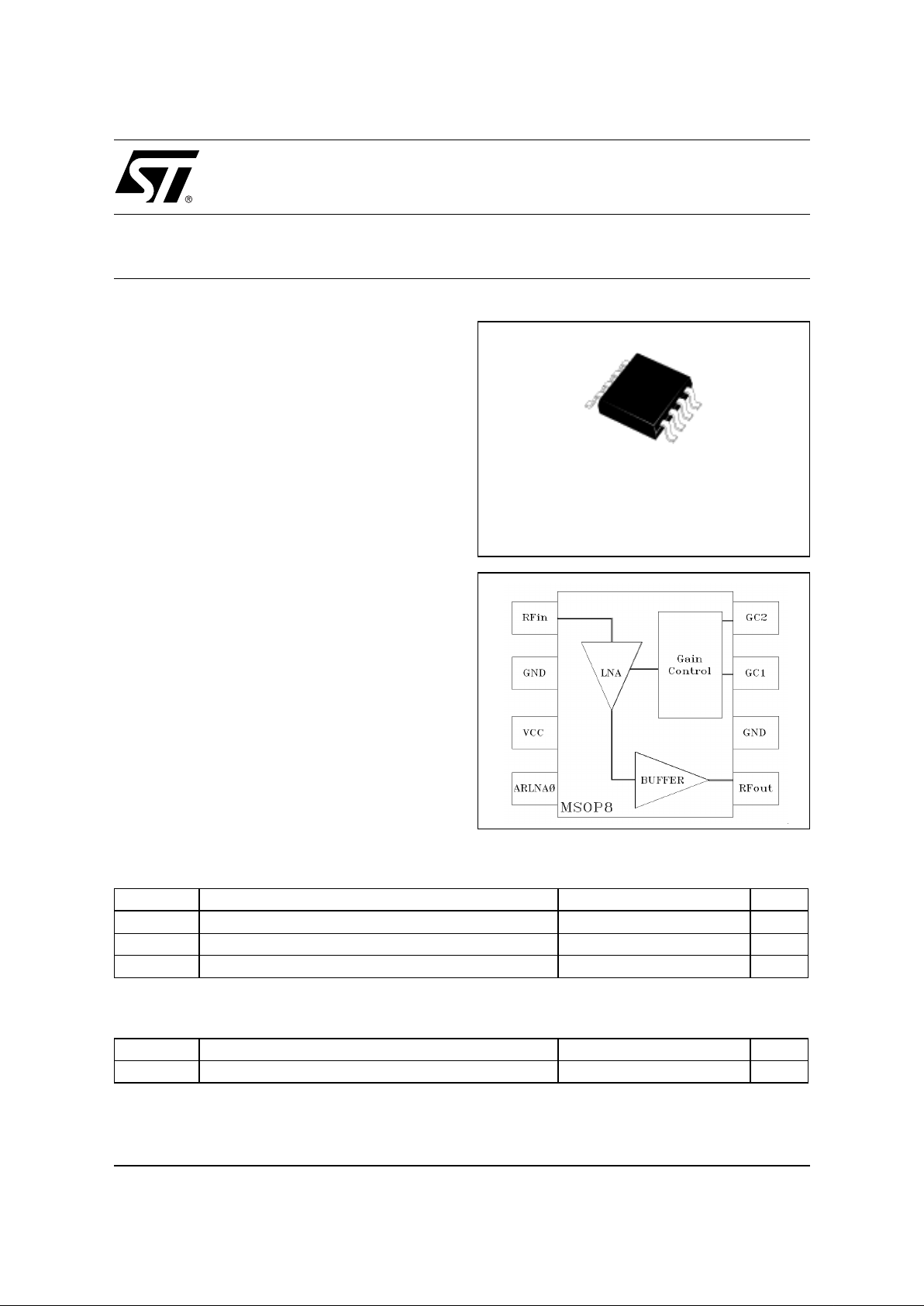
DESCRIPTION
The STB7002 is a Silicon monolithic amplifier, that
offers low noise figure and three gain levels for
1.8GHz applications. STB7002 is housed in a
small industry-standard MSOP8-EP surface
mount package, requiring very little board space
(50% reduction vs SO8 Package). MSOP8-EP
dimensions are 3mmx5mm with a 1.1mm
thickness. STB7002 is ESD protected and
requires minimum external components in the
application circuit, for the on-chip bias and gain
control. Furthermore, temperature and supply
voltage compensation ensu res high stability over
a wide range of operating conditions.
MSOP8-EP
(exposed pad)
ORDER CODE
STB7002
BRANDING
7002
ABSOLUTE MAXIMUM RATINGS
Symbol Parameter Value Unit
V
cc
Supply voltage 4 V
Tj Junction Temperature 150 °C
T
stg
Storage temperature -40 to +85 °C
THERMA L DA TA
Symbol Parameter Value Unit
R
th(j-a)
Junction -ambient Thermal Resistance TBD °C/W
Page 2
STB7002
2/7
ELECTRICAL SPECIFICATION (T
amb
= 25°C, Vcc = 2.8V)
Note(1) : Gp1 m in gain, Gp2 mid gain and Gp3 max gain.
Symbol Parameters Test Conditions Min. Typ. Max. Unit
Vcc Supply voltage 2.7 2.8 2.9 V
I
bias
Bias current
for G
p1
(1)
G
p2
(1)
G
p3
(1)
8
14
10
11.5
17.5
15.0
15.0
22.519mA
Istby
Standby current 20 µA
f Frequency range 1805 1880 MHz
G
p1,2,3
Power gain
G
p1
G
p2
G
p3
-3.0
16.0
24.0
0.0
18.0
26.0
3.0
20.0
28.0
dB
NF
1,2,3
Noise figure
for G
p1
G
p2
G
p3
9
2.9
2.6
dB
P1dB
1,2,3
Input 1 dB Compr.Power
for G
p1
G
p2
G
p3
-15.5
-19
-27
dBm
IIP3
1,2,3
Input Third Order Intercept
for G
p1
G
p2
G
p3
-4
-9
-17
dBm
VSWRi
Input VSWR
for G
p1
G
p2
G
p3
2.5:1
2.2:1
1.5:1
VSWRo
Output VSWR
for G
p1
G
p2
G
p3
1.3:1
1.5:1
1.8:1
AZout Zout LNA on/off 15 %
PINOUT
Pin Number Symbol Description Evaluation circuit components
1 RFin RF input L2 = 3.3nH, C2 =0.5pF
2 Gnd Ground
3 Vcc Voltage supply C4 = 4pF, L1 = 110nH, C7 = 10nF
4 ARLNA0 Enable for power down C3 = 10nF
5 RFout RF output C9 = 3pf, L3 = 5.6nH, C10 = 10nF, C11 = 100pF, L4 = 110nH
6 Gnd Ground
7 GC1 Gain selection C5 = 10nF
8 GC2 Gain selection C8 = 10nF
GAIN SELECTI0 N
G
p1Gp2Gp3
GC1 001
GC2 011
Page 3
3/7
STB7002
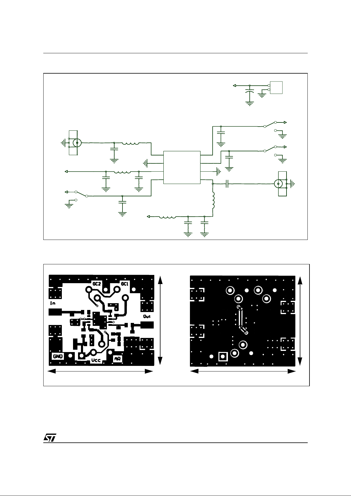
TEST CIRCUIT SCHEMATIC
RF_IN
1
GND
2
VCC
3
ARLNA0
4
GC2
8
GC1
7
GND
6
RF_OUT
5
STB7002
U1
C4
4p
C7
10n
C2
0.5p
C8
10n
C5
10n
C9
3p
C10
10n
C11
100p
C3
10n
L1
110n
L2
3.3n
*
VCC
L3
5.6n
L4
110n
VCC
1
2
JP1
BIAS
C6
4u7
VCC
S2
SW SPDT
S1
SW SPDT
S3
SW SPDT
VCC
VCC
VCC
J1
SMA_IN
J2
SMA_OUT
RF_IN
1
GND
2
VCC
3
ARLNA0
4
GC2
8
GC1
7
GND
6
RF_OUT
5
STB7002
U1
C4
4p
C7
10n
C2
0.5p
C8
10n
C5
10n
C9
3p
C10
10n
C11
100p
C3
10n
L1
110n
L2
3.3n
*
VCC
L3
5.6n
L4
110n
VCC
1
2
JP1
BIAS
C6
4u7
VCC
S2
SW SPDT
S1
SW SPDT
S3
SW SPDT
VCC
VCC
VCC
J1
SMA_IN
J2
SMA_OUT
TEST CIRCUIT PHOTOMASTER (board dimention s 23.5x20. 3mm )
BOTTOM VIEW
23.5mm
20.3mm
TOP VIEW
23.5mm
20.3mm
Page 4

STB7002
4/7
MAX GAI N
Freq. VSWRi VSWRo Isolation Gain
1802 1.48 1.94 -36.91 24.83
1813 1.45 1.94 -36.37 24.79
1824 1.43 1.94 -35.51 24.76
1835 1.41 1.93 -35.14 24.75
1846 1.38 1.92 -34.95 24.74
1857 1.36 1.91 -34.03 24.71
1868 1.35 1.89 -34.17 24.68
1879 1.33 1.87 -33.08 24.59
1890 1.32 1.84 -33.53 24.52
1901 1.30 1.83 -32.87 24.45
1912 1.29 1.79 -33.03 24.38
1923 1.28 1.77 -32.55 24.29
MID GAI N
Freq. VSWRi VSWRo Isolation Gain
1802 2.14 1.67 -36.70 18.32
1813 2.15 1.68 -36.07 18.33
1824 2.14 1.69 -35.58 18.34
1835 2.14 1.69 -35.13 18.37
1846 2.13 1.69 -34.51 18.40
1857 2.12 1.69 -33.92 18.43
1868 2.11 1.68 -33.38 18.45
1879 2.10 1.68 -32.30 18.42
1890 2.10 1.67 -33.39 18.41
1901 2.09 1.66 -32.80 18.39
1912 2.08 1.65 -32.72 18.35
1923 2.08 1.63 -32.20 18.32
INPUT/OUTPUT VSWR, ISOLATION AND GAIN PARAMETERS (MEASURED DATA)
Page 5

5/7
STB7002
MIN GAI N
Freq. VSWRi VSWRo Isolation Gain
1802 2.26 1.21 -34.63 1.9 7
1813 2.30 1.21 -34.45 1.9 3
1824 2.33 1.21 -33.83 1.8 9
1835 2.36 1.21 -33.57 1.8 6
1846 2.38 1.22 -32.99 1.8 2
1857 2.41 1.22 -32.3 1.79
1868 2.43 1.22 -31.94 1.7 6
1879 2.46 1.22 -31.55 1.7 0
1890 2.48 1.22 -31.91 1.6 6
1901 2.50 1.22 -31.52 1.6 3
1912 2.52 1.22 -31.34 1.5 8
1923 2.53 1.22 -31.09 1.5 3
Page 6

STB7002
6/7
MSOP8-EP MECHANICAL DATA
MIN. MAX MIN. MAX
A 0.037 0.043 0.94 1.10
A1 0.002 0.006 0.05 0.15
B 0.010 0.014 0.25 0.36
C 0.005 0.007 0.13 0.18
D 0.116 0.120 2.95 3.05
e
E 0.1 16 0.120 2.95 3.05
H 0.188 0.198 4.78 5.03
L 0.016 0.026 0.41 0.66
α
0° 6° 0° 6°
*X 0.087 0.099 2.210 2.515
*Y 0.062 0.074 1.575 1.880
Inch. mm
0.0256 BSC 0.65 BSC
Page 7

7/7
STB7002
Information furnished is believed to be accurate an d rel i able. However, STMicroelectronics assum es no responsibility for the co nsequences
of use of such information nor for any infringement of patents or other rights of third parties which may result from its use. No license is granted
by implic ation or otherwise under any patent or patent ri ghts of STM i croelectr onics. Sp ecifications menti oned in thi s publicati on are subject
to change without notice. This publication supersedes and replaces all information previously supplied. STMicroelectronics produ ct s are not
authorized for use as cri tical comp onents in lif e support devi ces or systems without express writ t en approval of STM i croelectronics.
The ST logo i s registered trademark of STMicroelectronics
2002 STMicroel ectronics - All Rights Reserved
All other names are the property of their respective ow ners.
STMicroelectroni cs GROUP OF COMPANIES
Australi a - B razil - Canada - China - Finland - France - Germany - Hong K ong - India - Israel - Italy - Japan -
Malaysia - Malta - Morocco - Singapore - Spain - Sweden - Switzerland - United Kingdom - U.S.A.
htt
p
://www.st.com
 Loading...