

Page 1
STB6NB50
N - CHANNEL 500V - 1.35Ω - 5.8A - D2PAK/I2PAK
PowerMESH MOSFET
TYPE V
DSS
R
DS(on)
I
D
STB6NB50 500 V < 1.5 Ω 5.8 A
■ TYPICALR
■ EXTREMELYHIGH dv/dtCAPABILITY
■ 100%AVALANCHETESTED
■ VERYLOW INTRINSIC CAPACITANCES
■ GATECHARGE MINIMIZED
DS(on)
= 1.35 Ω
DESCRIPTION
Using the latesthigh voltage MESH OVERLAY
process, STMicroelectronics has designed an
advanced family of power MOSFETs with
outstanding performances. The new patent
pending strip layout coupled with the Company’s
proprietary edge termination structure, gives the
lowest RDS(on) per area, exceptional avalanche
and dv/dt capabilities and unrivalled gate charge
and switching characteristics.
APPLICATIONS
■ HIGHCURRENT, HIGH SPEED SWITCHING
■ SWITCHMODE POWER SUPPLIES(SMPS)
■ DC-AC CONVERTERS FOR WELDING
EQUIPMENTAND UNINTERRUPTIBLE
POWERSUPPLIESAND MOTORDRIVE
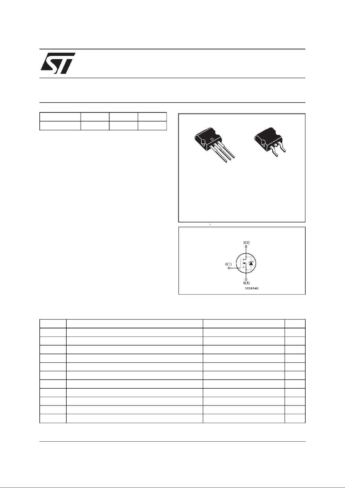
3
1
1
I2PAK
TO-262
(suffix”-1”)
3
2
D2PAK
TO-263
(Suffix ”T4”)
INTERNAL SCHEMATIC DIAGRAM
ABSOLUTE MAXIMUM RATINGS
Symbol Parameter Value Unit
V
V
V
I
DM
P
dv/ dt(
T
(•) Pulse width limited by safeoperating area (1)I
November 1999
Drain-source Voltage (VGS=0) 500 V
DS
Dra in- gate Volt age (RGS=20kΩ)
DGR
Gate -sourc e Volta ge
GS
I
Drain C urrent (co ntinuous) at Tc=25oC5.8A
D
I
Drain C urrent (co ntinuous) at Tc=100oC3.7A
D
500 V
30 V
±
(•) Drain C urrent (pu lsed) 23.2 A
Total Dissipation at Tc=25oC100W
tot
Derating Factor 0.8 W/
1) Peak Dio de Recovery volt age slope 4.5 V/ns
St orage T e m pe rature -65 t o 150
stg
T
Max. Op erating Junctio n T e m pe rat ure 150
j
≤
6A, di/dt≤200 A/µs, V
SD
≤
DD
V
(BR)DSS
,Tj≤T
JMAX
o
C
o
C
o
C
1/9
Page 2

STB6NB50
THERMAL DATA
R
thj-case
Rthj-a mb
R
thc-sink
T
AVALANCHE CHARACTERISTICS
Symbol Para meter Max Val ue Uni t
I
AR
E
Ther mal Resis t an ce Junc ti on-cas e Max
Ther mal Resis t an ce Junc ti on-ambien t Max
Thermal Resistance Case-sink Typ
Maximum Lead Tem peratu re Fo r Sold er ing Pur p os e
l
Avalanche Cur rent, Repetit iv e or No t- Re petitiv e
(pulse width limited by T
Single Pulse Avalanche Energy
AS
(starting T
=25oC, ID=IAR,VDD=50V)
j
max)
j
1.25
62.5
0.5
300
5.8 A
290 mJ
o
C/W
oC/W
o
C/W
o
C
ELECTRICAL CHARACTERISTICS (T
=25oC unless otherwisespecified)
case
OFF
Symbol Parameter Test Conditions Min. Typ. Max. Unit
V
(BR)DSS
Drain-sourc e
=250µAVGS=0
I
D
500 V
Break d own V o lt age
I
DSS
I
GSS
Zero Gate Voltage
Drain Cu rr ent (V
GS
Gat e- b ody Le aka ge
Current (V
DS
=0)
=0)
V
=MaxRating
DS
= Max Rating Tc=125oC
V
DS
= ± 30 V
V
GS
1
50
± 100 nA
ON(∗)
Symbol Parameter Test Conditions Min. Typ. Max. Unit
V
GS(th)
Gate Threshold
V
DS=VGSID
= 250 µA
345V
Voltage
R
DS(on)
Static Drain-source On
VGS=10V ID= 2.9 A 1.35 1.5
Resistanc e
I
D(on)
On S t ate Drain Cu rr ent VDS>I
D(on)xRDS(on)max
5.8 A
VGS=10V
DYNAMIC
Symbol Parameter Test Conditions Min. Typ. Max. Unit
g
(∗)Forward
fs
Tr ansconduc tance
C
C
C
Input Cap ac i t an c e
iss
Out put Capacita nce
oss
Reverse Transfer
rss
Capacitance
VDS>I
D(on)xRDS(on)maxID
=2.9A 2.5 4 S
VDS=25V f=1MHz VGS=0 680
110
12
884
149
16
µA
µ
Ω
pF
pF
pF
A
2/9
Page 3

STB6NB50
ELECTRICAL CHARACTERISTICS
(continued)
SWITCHINGON
Symbol Parameter Test Conditions Min. Typ. Max. Unit
t
d(on)
Turn-on Time
r
Rise Time
t
VDD= 250 V ID=2.9A
R
=4.7
G
Ω
VGS=10V
11.5
8
16
12
(see test circuit, figure 3)
Q
Q
Q
Total Gate Charge
g
Gat e- Source Cha rge
gs
Gate-Drain Charge
gd
VDD= 400 V ID=5.8AVGS=10V 21
7.2
8
30 nC
SWITCHINGOFF
Symbol Parameter Test Conditions Min. Typ. Max. Unit
t
r(Voff)
t
t
Off -voltage Rise Time
Fall Time
f
Cross-ov er Time
c
VDD= 400 V ID=5.8A
=4.7 ΩVGS=10V
R
G
(see test circuit, figure 5)
7
5
15
12
10
23
SOURCEDRAINDIODE
Symbol Parameter Test Conditions Min. Typ. Max. Unit
I
SD
I
SDM
V
SD
t
Q
I
RRM
(∗) Pulsed: Pulse duration = 300 µs, dutycycle 1.5%
(•) Pulse width limited by safe operating area
Source-drain Curr ent
(•)
Source-drain Curr ent
5.8
23.2
(pulsed)
(∗) F or ward O n Voltage ISD=5.8A VGS=0 1.6 V
Reverse Recov er y
rr
Time
Reverse Recov er y
rr
=5.8A di/dt=100A/µs
I
SD
= 100 V Tj=150oC
V
DD
(see test circuit, figure 5)
435
3.3
Charge
Reverse Recov er y
15
Current
ns
ns
nC
nC
ns
ns
ns
A
A
ns
µ
A
C
SafeOperating Area ThermalImpedance
3/9
Page 4

STB6NB50
OutputCharacteristics
Transconductance
TransferCharacteristics
Static Drain-sourceOn Resistance
Gate Charge vs Gate-sourceVoltage
4/9
CapacitanceVariations
Page 5
STB6NB50
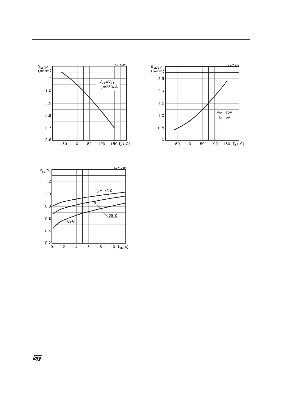
Normalized Gate ThresholdVoltage vs
Temperature
Source-drainDiode Forward Characteristics
Normalized On Resistancevs Temperature
5/9
Page 6

STB6NB50
Fig. 1:
UnclampedInductive Load Test Circuit
Fig. 3: Switching Times Test CircuitsFor
ResistiveLoad
Fig. 2:
UnclampedInductive Waveform
Fig. 4: Gate Charge test Circuit
Fig. 5:
Test CircuitFor InductiveLoad Switching
And Diode Recovery Times
6/9
Page 7

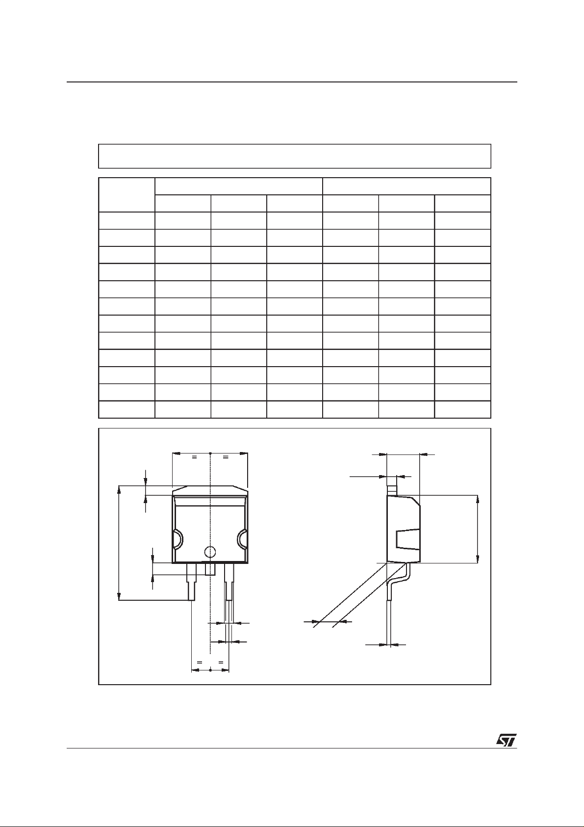
TO-262 (I2PAK) MECHANICAL DATA
STB6NB50
DIM.
MIN. TYP. MAX. MIN. TYP. MAX.
A 4.3 4.6 0.169 0.181
A1 2.49 2.69 0.098 0.106
B 0.7 0.93 0.027 0.036
B1 1.2 1.38 0.047 0.054
B2 1.25 1.4 0.049 0.055
C 0.45 0.6 0.017 0.023
C2 1.21 1.36 0.047 0.053
D 8.95 9.35 0.352 0.368
e 2.44 2.64 0.096 0.104
E 10 10.28 0.393 0.404
L 13.2 13.5 0.519 0.531
L1 3.48 3.78 0.137 0.149
L2 1.27 1.4 0.050 0.055
mm inch
CA1
A
C2
B2
B
e
E
L1
L2
D
L
P011P5/C
7/9
Page 8
STB6NB50
TO-263(D2PAK) MECHANICALDATA
DIM.
MIN. TYP. MAX. MIN. TYP. MAX.
A 4.3 4.6 0.169 0.181
A1 2.49 2.69 0.098 0.106
B 0.7 0.93 0.027 0.036
B2 1.25 1.4 0.049 0.055
C 0.45 0.6 0.017 0.023
C2 1.21 1.36 0.047 0.053
D 8.95 9.35 0.352 0.368
E 10 10.28 0.393 0.404
G 4.88 5.28 0.192 0.208
L 15 15.85 0.590 0.624
L2 1.27 1.4 0.050 0.055
L3 1.4 1.75 0.055 0.068
mm inch
E
A
C2
8/9
L2
D
L
L3
B2
B
A1
C
G
P011P6/C
Page 9

STB6NB50
Information furnished is believed tobeaccurateand reliable.However, STMicroelectronics assumes no responsibilityforthe consequences
of use of such information nor for any infringement of patents or other rights of third parties which may result from its use. No license is
granted by implication or otherwise under any patent or patent rights ofSTMicroelectronics. Specificationmentioned in this publication are
subjecttochange without notice. This publicationsupersedesandreplaces all information previouslysupplied. STMicroelectronicsproducts
are not authorized for use as critical components in life support devices or systemswithout express written approval of STMicroelectronics.
The ST logo is a trademark of STMicroelectronics
1999 STMicroelectronics – Printed in Italy – All Rights Reserved
STMicroelectronics GROUP OF COMPANIES
Australia - Brazil - China - Finland - France - Germany - Hong Kong - India - Italy - Japan - Malaysia - Malta - Morocco -
Singapore - Spain - Sweden - Switzerland - United Kingdom - U.S.A.
http://www.st.com
.
9/9
 Loading...