

Page 1
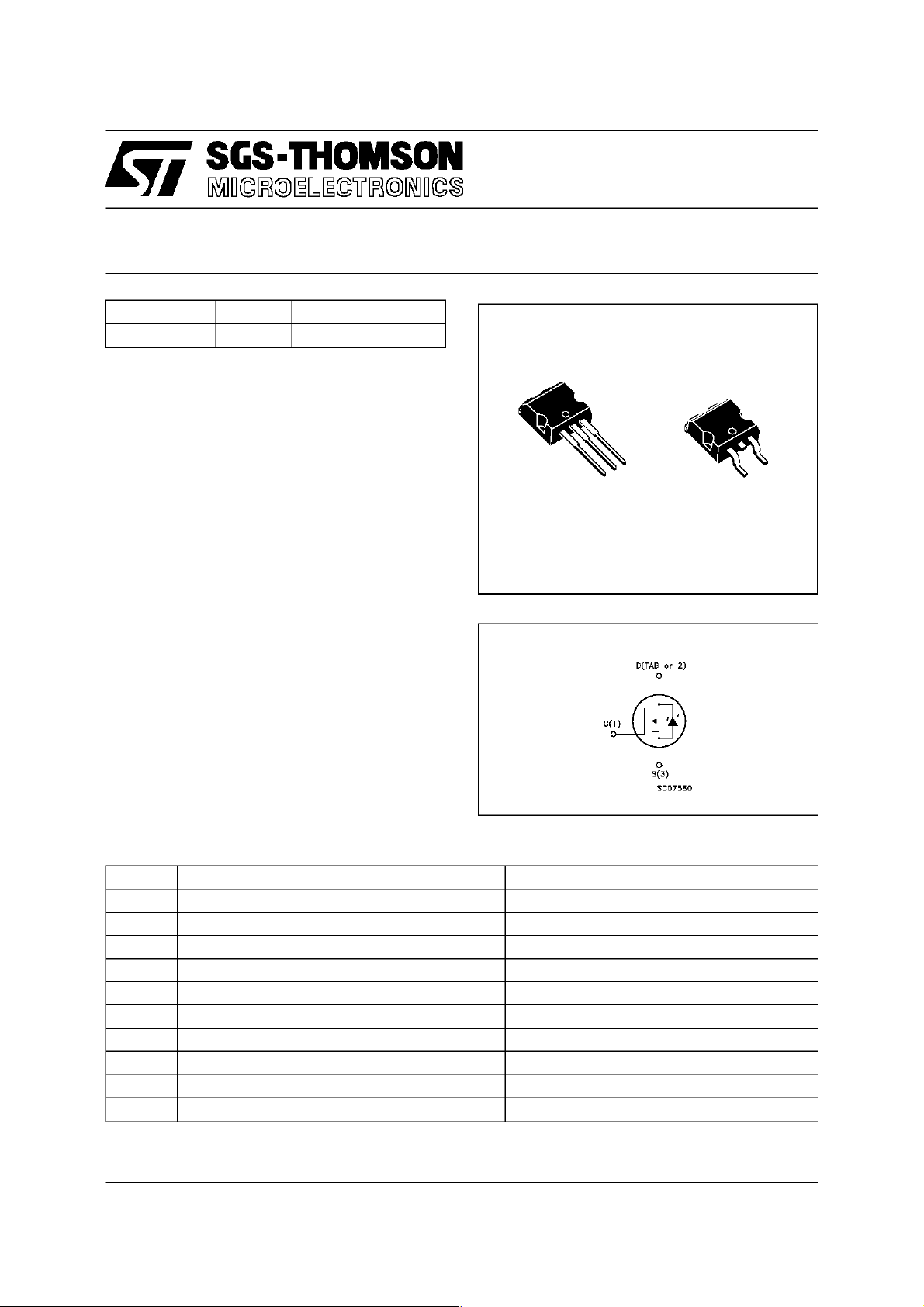
STB6NA60
N - CHANNEL ENHANCEMENT MODE
FAST POWER MOS TRANSISTOR
TYPE V
DSS
R
DS(on )
I
D
STB 6NA60 600 V < 1.2 Ω 6.5 A
TYPICALR
±30V GATE TO SOURCE VOLTAGE RATING
100% AVALANCHETESTED
REPETITIVEAVALANCHEDATAAT100
LOW INTRINSIC CAPACITANCES
GATECHARGE MINIMIZED
REDUCEDTHRESHOLD VOLTAGESPREAD
THROUGH-HOLEI2PAK (TO-262) POWER
DS(on)
=1Ω
o
C
PACKAGEIN TUBE(SUFFIX ”-1”)
SURFACE-MOUNTING D2PACK (TO-263)
POWERPACKAGEIN TUBE(NO SUFFIX)
OR IN TAPE& REEL(SUFFIX ”T4”)
APPLICATIONS
HIGH CURRENT, HIGHSPEED SWITCHING
SWITCHMODE POWER SUPPLIES(SMPS)
DC-AC CONVERTERSFOR WELDING
EQUIPMENTANDUNINTERRUPTIBLE
POWERSUPPLIESAND MOTOR DRIVE
3
2
1
I2PAK
TO-262
1
D2PAK
TO-263
INTERNAL SCHEMATIC DIAGRAM
3
ABSOLUTE MAXIMUM RATINGS
Symbol Parameter Val ue Uni t
V
V
V
I
DM
P
T
(•) Pulsewidth limitedby safe operating area
October 1995
Drain-source Voltage (VGS= 0) 600 V
DS
Drain- gate Volt age (RGS=20kΩ) 600 V
DGR
Gate-s ource Voltage ± 30 V
GS
I
Drain Cur rent (con t inuous) at Tc=25oC6.5A
D
I
Drain Cur rent (con t inuous) at Tc=100oC4.3A
D
(•) Drain Cur rent (pul sed) 26 A
Tot al Dis s ipation at Tc=25oC 125 W
tot
Derat ing Fa ct or 1 W/
Sto rage Tem perature -65 t o 150
stg
T
Max. O per ating Junc t i on Tem perat u r e 150
j
o
o
o
C
C
C
1/10
Page 2
STB6NA60
THERMAL DATA
R
thj-case
R
thj-amb
R
thc-sink
T
AVALANCHE CHARACTERISTICS
Symb ol Param et er Max Val ue Unit
I
AR
E
E
I
AR
Therm al Resistanc e Juncti on-c ase Max
Therm al Resistanc e Juncti on-am b ient Max
Therm al Resistanc e Case-sink Ty p
Maxim um Lead T em p erat ur e For Soldering Purpose
l
Avalanc h e Current , Repet it ive or Not - Rep et it i v e
(pulse w idt h lim i te d by T
Single P ulse A v al anc he E ne r gy
AS
(starting T
Repetit ive Avalan che E ner gy
AR
=25oC, ID=IAR,VDD=50V)
j
(pulse w idt h lim i te d by T
max, δ <1%)
j
max, δ <1%)
j
Avalanc h e Current , Repet it ive or Not - Rep et it i v e
=100oC, pulse widt h limi t ed by Tjmax, δ <1%)
(T
c
1
62.5
0.5
300
6.5 A
215 mJ
9.5 mJ
4.3 A
o
C/W
o
C/W
o
C/W
o
C
ELECTRICAL CHARACTERISTICS (T
=25oC unlessotherwise specified)
case
OFF
Symb ol P ar ameter Test Co ndi t ion s Min. Typ . Max. Unit
V
(BR)DSS
Drain-s ource
ID= 250 µAVGS=0 600 V
Break down Vol t age
I
DSS
I
GSS
Zero G ate Voltage
Drain Current ( V
GS
Gat e- body Leakage
Current (V
DS
=0)
=0)
V
= M ax R at ing
DS
= M ax R at ing x 0.8 Tc=125oC
V
DS
V
= ± 30 V ± 100 nA
GS
250
1000µAµA
ON (∗)
Symb ol P ar ameter Test Co ndi t ion s Min. Typ . Max. Unit
V
GS(t h)
R
DS(on)
I
D(on)
Gat e Thr eshold Volt age VDS=VGSID= 250 µA 2.25 3 3.75 V
Sta t ic Drain-source O n
Resistance
VGS= 10V ID=3A
=10V ID=3A Tc=100oC
V
GS
On State Drain Cu rr ent VDS>I
D(on)xRDS(on)max
6.5 A
11.2
2.4
VGS=10V
DYNAMIC
Symb ol P ar ameter Test Co ndi t ion s Min. Typ . Max. Unit
g
(∗)Forward
fs
Tra nsconductance
C
C
C
Input Capacitance
iss
Out put Capac i t anc e
oss
Reverse Transfer
rss
Capacit an c e
VDS>I
D(on)xRDS(on)maxID
=3A 3.5 5.6 S
VDS=25V f=1MHz VGS= 0 1 150
155
40
1550
210
55
Ω
Ω
pF
pF
pF
2/10
Page 3
STB6NA60
ELECTRICAL CHARACTERISTICS (continued)
SWITCHING ON
Symb ol P ar ameter Test Co ndi t ion s Min. Typ . Max. Unit
t
d(on)
t
r
Turn-on Time
Rise Time
VDD= 300 V ID=3A
=47 Ω VGS=10V
R
G
(see t est cir cuit, figure 3)
(di/dt)
Turn-on Current Slope VDD= 480 V ID=6A
on
=47 Ω VGS=10V
R
G
(see t est cir cuit, figure 5)
Q
Q
Q
Total Ga te Charge
g
Gat e- Source Char ge
gs
Gate-Drain Charge
gd
VDD=480V ID=3A VGS=10V 54
SWITCHING OFF
Symb ol P ar ameter Test Co ndi t ion s Min. Typ . Max. Unit
t
r(Voff)
t
Off-voltage Rise Tim e
t
Fall Time
f
Cross-over Ti me
c
VDD= 480 V ID=6A
=47 Ω VGS=10V
R
G
(see t est cir cuit, figure 5)
SOURCEDRAIN DIODE
35
90
50
125
200 A/µs
75 nC
8
23
80
20
115
110
30
155
ns
ns
nC
nC
ns
ns
ns
Symb ol P ar ameter Test Co ndi t ion s Min. Typ . Max. Unit
I
SDM
I
SD
Source-drain Current
(•)
Source-drain Current
6.5
26
(pulsed)
(∗) F orward O n V olt ag e ISD=6.5A VGS=0 1.6 V
V
SD
t
Q
Revers e Recovery
rr
Time
Revers e Recovery
rr
ISD= 6 A di/dt = 100 A/ µs
=100V Tj=150oC
V
DD
(see t est cir cuit, figure 5)
600
9
Charge
I
RRM
Revers e Recovery
30
Current
(∗) Pulsed: Pulse duration =300 µs, duty cycle 1.5 %
(•) Pulse widthlimitedby safeoperating area
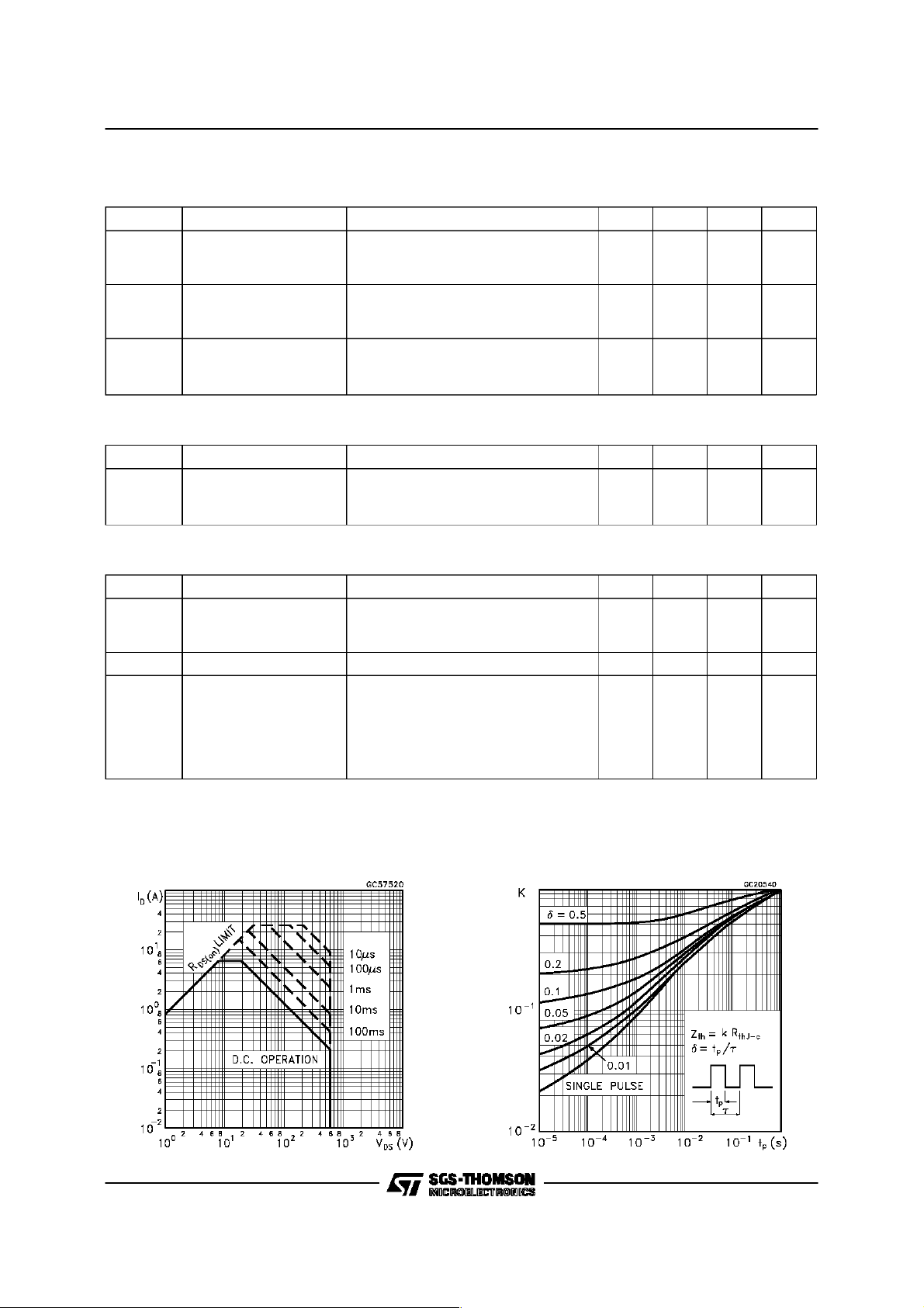
Safe Operating Area ThermalImpedance
A
A
ns
µC
A
3/10
Page 4

STB6NA60
Derating Curve
TransferCharacteristics
Output Characteristics
Transconductance
Static Drain-sourceOn Resistance
4/10
Gate Charge vs Gate-source Voltage
Page 5

STB6NA60
CapacitanceVariations
NormalizedOn Resistance vs Temperature
NormalizedGate Threshold Voltage vs
Temperature
Turn-onCurrent Slope
Turn-offDrain-sourceVoltageSlope
Cross-overTime
5/10
Page 6

STB6NA60
SwitchingSafe OperatingArea
Source-drainDiode Forward Characteristics
AccidentalOverloadArea
Fig. 1: UnclampedInductiveLoad TestCircuit
6/10
Fig. 2: Unclamped Inductive Waveform
Page 7

STB6NA60
Fig. 3: SwitchingTimes Test Circuits For
ResistiveLoad
Fig. 5: Test Circuit For Inductive Load Switching
And DIodeRecovery Times
Fig. 4: Gate Charge test Circuit
7/10
Page 8

STB6NA60
TO-262 (I2PAK) MECHANICAL DATA
DIM.
MIN. TYP. MAX. MIN. TYP. MAX.
A 4.3 4.6 0.169 0.181
A1 2.49 2.69 0.098 0.106
B 0.7 0.93 0.027 0.036
B1 1.2 1.38 0.047 0.054
B2 1.25 1.4 0.049 0.055
C 0.45 0.6 0.017 0.023
C2 1.21 1.36 0.047 0.053
D 9 9.35 0.354 0.368
e 2.44 2.64 0.096 0.104
E 10 10.28 0.393 0.404
L 13.2 13.5 0.519 0.531
L1 3.48 3.78 0.137 0.149
L2 1.27 1.37 0.050 0.054
mm inch
8/10
C
A
A1
C2
B2
B
e
E
L1
L2
D
L
Page 9

TO-263 (D2PAK) MECHANICAL DATA
STB6NA60
DIM.
MIN. TYP. MAX. MIN. TYP. MAX.
A 4.3 4.6 0.169 0.181
A1 2.49 2.69 0.098 0.106
B 0.7 0.93 0.027 0.036
B2 1.25 1.4 0.049 0.055
C 0.45 0.6 0.017 0.023
C2 1.21 1.36 0.047 0.053
D 9 9.35 0.354 0.368
E 10 10.28 0.393 0.404
G 4.88 5.28 0.192 0.208
L 15 15.85 0.590 0.624
L2 1.27 1.37 0.050 0.054
L3 1.4 1.75 0.055 0.068
mm inch
E
A
C2
L2
D
L
L3
B2
B
A1
C
G
9/10
Page 10

STB6NA60
Information furnished is believed to be accurateand reliable.However, SGS-THOMSON Microelectronics assumes no responsability for the
consequences of use of such informationnor forany infringement ofpatents or other rights of third parties which may results fromits use.No
licenseisgranted by implication orotherwise underanypatent orpatent rights ofSGS-THOMSON Microelectronics. Specifications mentioned
in this publicationare subjectto change without notice. Thispublicationsupersedes and replacesall information previouslysupplied.
SGS-THOMSON Microelectronicsproductsarenotauthorized for use ascriticalcomponentsin lifesupportdevices or systemswithoutexpress
writtenapproval of SGS-THOMSON Microelectonics.
1995 SGS-THOMSONMicroelectronics - All RightsReserved
Australia- Brazil - France- Germany - HongKong - Italy - Japan- Korea - Malaysia- Malta-Morocco- TheNetherlands-
Singapore- Spain- Sweden- Switzerland- Taiwan - Thailand - United Kingdom- U.S.A
SGS-THOMSONMicroelectronics GROUPOF COMPANIES
...
10/10
 Loading...