

Page 1
STB60NF03L
N-CHANNEL 30V - 0.008
TYPE V
ST B60NF03L 30 V < 0.01 Ω 60 A
■ TYPICALR
■ OPTIMIMIZED FOR HIGH SWITCHING
DS(on)
DSS
= 0.008 Ω
OPERATIONS
■ LOW THRESHOLDDRIVE
■ LOGICLEVEL GATE DRIVE
DESCRIPTION
This Power Mosfet is the latest development of
STMicroelectronics unique ”Single Feature
Size” strip-based process. The resulting
transistor shows extremely high packing density
for low on-resistance, rugged avalance
characteristics and less critical alignment steps
therefore a remarkable manufacturing
reproducibility.
APPLICATIONS
■ LOW VOLTAGEDC-DC CONVERTERS
■ HIGHCURRENT, HIGHSPEED SWITCHING
■ HIGHEFFICIENCY SWITCHINGCIRCUITS
R
DS(on)
I
D
Ω
- 60A D2PAK
STripFET POWER MOSFET
PRELIMINARY DATA
3
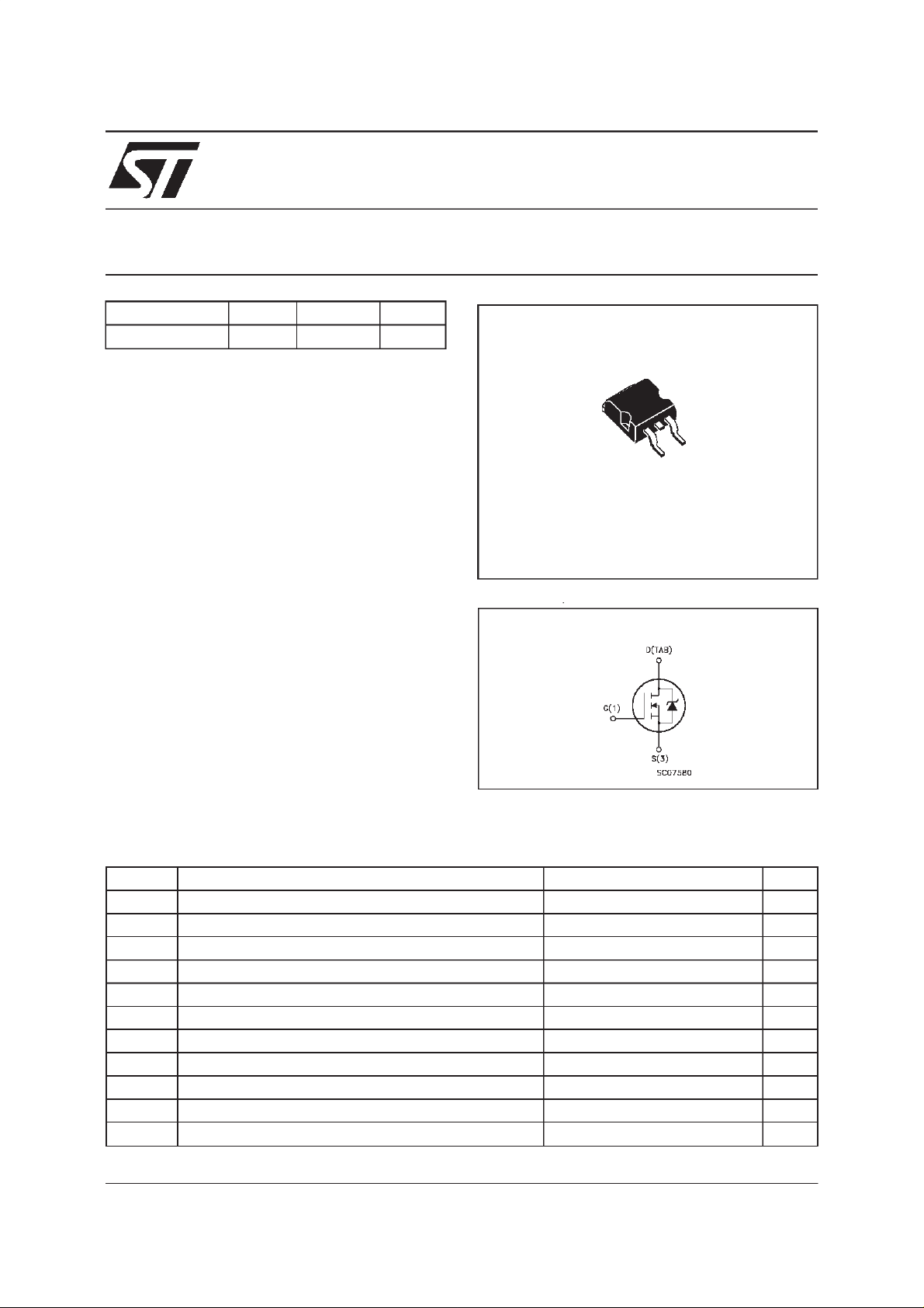
1
D2PAK
TO-263
ADD SUFFIX ”T4” FOR ORDERING IN TAPE & REEL
INTERNAL SCHEMATIC DIAGRAM
ABSOLUTE MAXIMUM RATINGS
Symbol Parameter Value Unit
V
V
V
I
DM
P
E
AS(1
T
(•) Pulse width limited by safeoperating area (1) starting Tj
September 1999
Dra in- sour c e Volt age ( VGS=0) 30 V
DS
Dra in- gate V ol t age (RGS=20kΩ)30V
DGR
Gat e-source Voltage
GS
I
Dra in Current ( continuous ) a t Tc=25oC60A
D
I
Dra in Current ( continuous ) a t Tc=100oC42A
D
(•) Dra in Current ( p uls ed ) 240 A
Tot al Dissipat ion at Tc=25oC 100 W
tot
Der ati ng Fac t or 0.67 W/
) Single Puls e Av alan che Energy 650 mJ
St orage Tempe rat ure -65 t o 175
stg
T
Max. O perating Junc t ion T emperat ure 175
j
=25oC,ID=30A,VDD= 20V
20 V
±
o
C
o
C
o
C
1/6
Page 2

STB60NF03L
THERMAL DATA
R
thj-case
R
thj-amb
T
Ther mal Resistanc e Junct ion-case Max
Ther mal Resistanc e Junct ion-ambient Max
Maximum Lead Temperature For Solder ing Purpose
l
1.5
62.5
300
o
C/W
o
C/W
o
C
ELECTRICAL CHARACTERISTICS
=25oC unless otherwisespecified)
(T
case
OFF
Symbol Parameter Test Conditions Min. Typ. Max. Unit
V
(BR)DSS
Drain-source
ID=250µAVGS=0 30 V
Break dow n V o lt age
I
DSS
I
GSS
Zero Gate Voltage
Drain Curr e nt (V
GS
Gat e- bod y L eakag e
Current (V
DS
=0)
=0)
V
=MaxRating
DS
=MaxRating Tc=125oC
V
DS
V
= ± 20 V ± 100 nA
GS
1
10
ON(∗)
Symbol Parameter Test Conditions Min. Typ. Max. Unit
V
GS(th)
R
DS(on)
I
D(on)
Gate Threshold Voltage VDS=VGSID= 250 µA11.52.5V
Sta t ic Drain -s our c e O n
Resistance
On State Drain Current VDS>I
VGS=10V ID=30A
V
=4.5V ID=30A
GS
D(on)xRDS(on)max
0.008
0.0095
0.01
0.015
60 A
VGS=10V
DYNAMIC
Symbol Parameter Test Conditions Min. Typ. Max. Unit
g
(∗)Forward
fs
Tr ansc on duc tance
C
C
C
Input Capacitance
iss
Out put Capacitance
oss
Reverse Tr ansfer
rss
Capacit a nc e
VDS>I
D(on)xRDS(on)maxID
=30 A 60 S
VDS=25V f=1MHz VGS= 0 2550
630
215
µA
µ
Ω
Ω
pF
pF
pF
A
2/6
Page 3

STB60NF03L
ELECTRICAL CHARACTERISTICS
(continued)
SWITCHING ON
Symbol Parameter Test Conditions Min. Typ. Max. Unit
t
d(on)
t
Tur n-on Delay Time
Rise Ti me
r
VDD=15V ID=30A
R
=4.7
G
Ω
VGS=4.5V
40
250
(Resis t iv e Loa d, s ee fig. 3 )
Q
Q
Q
Tot al Gat e Charge
g
Gat e- Source Charg e
gs
Gate-Drain Charge
gd
VDD=24V ID=60A VGS=5V 43
12
21
58 nC
SWITCHING OFF
Symbol Parameter Test Conditions Min. Typ. Max. Unit
t
d(off)
Tur n-of f Delay Time
t
Fall T ime
f
VDD=15V ID=30A
=4.7 Ω VGS=4.5V
R
G
60
70
(Resis t iv e Loa d, s ee fig. 3 )
SOURCEDRAINDIODE
Symbol Parameter Test Conditions Min. Typ. Max. Unit
I
V
I
SDM
SD
Q
I
RRM
SD
t
Source-drain Current
(•)
Source-drain Current
60
240
(pulsed)
(∗)ForwardOnVoltage ISD=60A VGS=0 1.5 V
Reverse Recovery
rr
Time
Reverse Recovery
rr
ISD= 60 A di/dt = 100 A/ µ s
=15V Tj=150oC
V
DD
(see test circuit, fig. 5)
75
100
Charge
Reverse Recovery
2.6
Current
ns
ns
nC
nC
ns
ns
A
A
ns
nC
A
(∗) Pulsed: Pulse duration = 300µs, duty cycle 1.5 %
(•) Pulse width limited by safe operatingarea
3/6
Page 4

STB60NF03L
Fig. 1:
UnclampedInductiveLoad TestCircuit
Fig. 3: SwitchingTimes Test Circuits For
ResistiveLoad
Fig. 2:
UnclampedInductive Waveform
Fig. 4: Gate Chargetest Circuit
Fig. 5:
Test CircuitFor InductiveLoad Switching
And Diode Recovery Times
4/6
Page 5

TO-263 (D2PAK) MECHANICAL DATA
STB60NF03L
DIM.
MIN. TYP. MAX. MIN. TYP. MAX.
A 4.4 4.6 0.173 0.181
A1 2.49 2.69 0.098 0.106
B 0.7 0.93 0.027 0.036
B2 1.14 1.7 0.044 0.067
C 0.45 0.6 0.017 0.023
C2 1.21 1.36 0.047 0.053
D 8.95 9.35 0.352 0.368
E 10 10.4 0.393 0.409
G 4.88 5.28 0.192 0.208
L 15 15.85 0.590 0.624
L2 1.27 1.4 0.050 0.055
L3 1.4 1.75 0.055 0.068
mm inch
D
A
C2
DETAIL”A”
C
A2
DETAIL”A”
A1
B2
E
L2
L
L3
B
G
P011P6/E
5/6
Page 6

STB60NF03L
Information furnishedis believedto be accurateand reliable.However, STMicroelectronics assumes no responsibilityfor the consequences
of use of such information nor for any infringement of patents or other rights of third parties which may result from its use. No license is
granted by implication or otherwise under any patent or patent rights ofSTMicroelectronics. Specificationmentioned in this publication are
subjectto change without notice.Thispublicationsupersedes and replacesall informationpreviouslysupplied. STMicroelectronicsproducts
are not authorized for use as critical components in life support devicesor systemswithout express written approvalof STMicroelectronics.
The STlogo is a trademark of STMicroelectronics
1999 STMicroelectronics – Printed in Italy – All Rights Reserved
STMicroelectronics GROUP OF COMPANIES
Australia - Brazil - China - Finland - France - Germany - Hong Kong - India - Italy - Japan - Malaysia - Malta - Morocco -
6/6
Singapore - Spain - Sweden - Switzerland - United Kingdom - U.S.A.
http://www.st.com
.
 Loading...