

Page 1
STB60NE06L-16
N - CHANNEL 60V - 0.014Ω - 60A D2PAK
STripFET POWER MOSFET
TYPE V
DSS
R
DS(on)
I
D
ST B60NE06L-16 60 V < 0.16 Ω 60 A
■ TYPICALR
■ AVALANCHERUGGEDTECHNOLOGY
■ LOW GATE CHARGE
■ HIGHCURRENT CAPABILITY
■ 175
■ LOW THRESHOLDDRIVE
■ FORTHROUGH-HOLE VERSION CONTACT
o
C OPERATINGTEMPERATURE
DS(on)
= 0.014 Ω
SALESOFFICE
DESCRIPTION
This Power Mosfet is the latest development of
STMicroelectronisunique ”Single Feature Size”
strip-based process. The resulting transistor
shows extremely high packing density for low
on-resistance, rugged avalance characteristics
and less critical alignment steps therefore a
remarkablemanufacturingreproducibility.
APPLICATIONS
■ HIGHCURRENT, HIGH SPEED SWITCHING
■ SOLENOIDAND RELAYDRIVERS
■ DC-DC& DC-ACCONVERTERS
■ AUTOMOTIVEENVIRONMENT
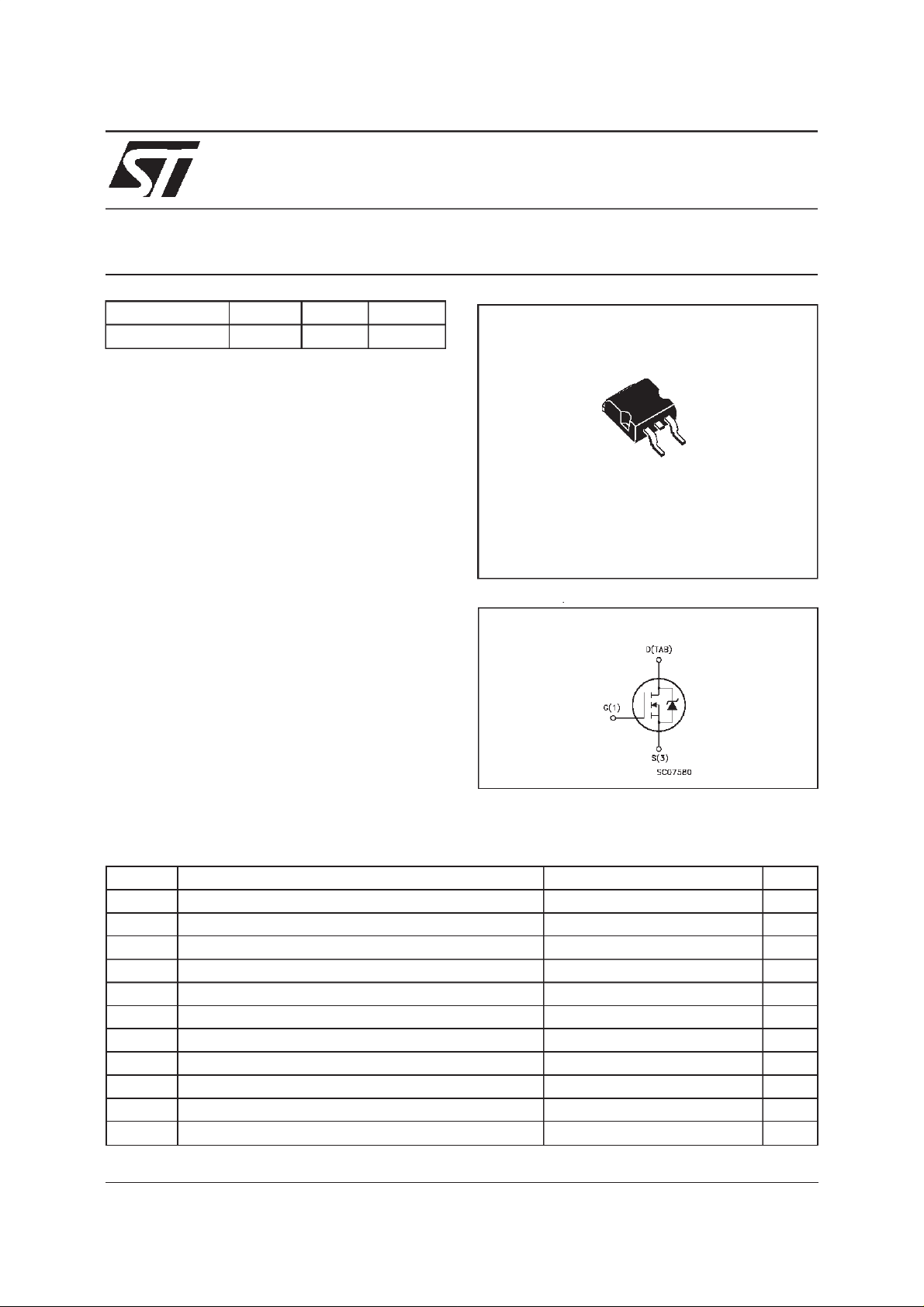
3
1
D2PAK
TO-263
(suffix ”T4”)
INTERNAL SCHEMATIC DIAGRAM
ABSOLUTE MAXIMUM RATINGS
Symbol Parameter Value Unit
V
V
V
I
DM
P
dv/ dt Peak Diode Re c overy v olt age slope 1 V/ns
T
(•) Pulsewidth limited by safeoperating area (1)ISD≤60 A, di/dt ≤ 300 A/µs, VDD≤ V
May 2000
Dra in- sour c e Vol t age (VGS=0) 60 V
DS
Dra in- gate Voltage (RGS=20kΩ)60V
DGR
Gat e-source Voltage
GS
I
Dra in Current ( continuous) at Tc=25oC60A
D
I
Dra in Current ( continuous) at Tc=100oC42A
D
15 V
±
(•) Dra in Current ( p uls ed ) 240 A
Tot al Diss ipation at Tc=25oC 150 W
tot
Derating Factor 1 W/
St orage T empe r at ure -65 to 175
stg
T
Max. Operat ing Junction Tem perature 175
j
(BR)DSS,Tj≤TJMAX
o
C
o
C
o
C
1/8
Page 2
STB60NE06L-16
THERMAL DATA
R
thj-case
Rthj-amb
R
thc-sink
T
AVALANCHE CHARACTERISTICS
Symbol Parameter Max Value Unit
I
AR
E
Ther mal Resistanc e Junct ion-case Max
Ther mal Resistanc e Junct ion-ambient Max
Ther mal Resistanc e Case-sink Ty p
Maximum L ead Temperat ur e For Solder ing Purp ose
l
Avalanche Current, Repetitive or Not-Repetitive
(pulse width limited by T
Single Pulse A valanche Energy
AS
(starting T
=25oC, ID=IAR,VDD=25V)
j
max)
j
1
62.5
0.5
300
60 A
400 mJ
o
C/W
o
C/W
o
C/W
o
C
ELECTRICAL CHARACTERISTICS
=25oC unless otherwisespecified)
(T
case
OFF
Symbol Parameter Test Conditions Min. Typ. Max. Unit
V
(BR)DSS
Drain-source
ID=250µAVGS=0 60 V
Break dow n Voltage
I
DSS
I
GSS
Zero Gate Voltage
Drain Current (V
GS
Gat e- bod y Leakage
Current (V
DS
=0)
=0)
V
=MaxRating
DS
=MaxRating Tc= 125oC
V
DS
V
=± 15 V
GS
1
10
100 nA
±
ON(∗)
Symbol Parameter Test Conditions Min. Typ. Max. Unit
V
GS(th)
R
DS(on)
I
D(on)
Gate Threshold Voltage VDS=VGSID= 250 µ A11.62.5V
Sta t ic Drain-sour ce On
Resistance
VGS=5V ID=30A
=10V ID=30A
V
GS
On State Drain Current VDS>I
D(on)xRDS(on )max
0.014
0.012
60 A
0.016
0.014ΩΩ
VGS=10V
DYNAMIC
Symbol Parameter Test Conditions Min. Typ. Max. Unit
g
(∗)Forward
fs
Tr ansc on duc tance
C
C
C
Input Capacitance
iss
Out put Capacitance
oss
Reverse Transfer
rss
Capacit a nc e
VDS>I
D(on)xRDS(on )maxID
=30 A 30 S
VDS=25V f=1MHz VGS= 0 4150
590
150
µ
µA
pF
pF
pF
A
2/8
Page 3
STB60NE06L-16
ELECTRICAL CHARACTERISTICS
(continued)
SWITCHINGON
Symbol Parameter Test Conditions Min. Typ. Max. Unit
t
d(on)
t
Tur n-on Delay T ime
Rise Time
r
VDD=30V ID=30A
R
=4.7 W VGS=5V
G
50
155
(see test circuit, figure 3)
Q
Q
Q
Tot al Gate Charge
g
Gat e- Source Charge
gs
Gate-Drain Charge
gd
VDD=40V ID=60A VGS=5V 55
15
30
70 nC
SWITCHINGOFF
Symbol Parameter Test Conditions Min. Typ. Max. Unit
t
r(Voff)
t
t
Off-volt age Rise Tim e
Fall T ime
f
Cross-over Time
c
VDD=48V ID=20A
=4.7 Ω VGS=5V
R
G
(see test circuit, figure 5)
45
220
280
SOURCEDRAINDIODE
Symbol Parameter Test Conditions Min. Typ. Max. Unit
I
SD
I
SDM
V
SD
t
Q
I
RRM
(∗) Pulsed:Pulse duration = 300µs, duty cycle 1.5%
(•) Pulse width limited by safeoperating area
Source-drain Current
(•)
Source-drain Current
60
240
(pulsed)
(∗)ForwardOnVoltage ISD=60A VGS=0 1.5 V
Reverse Recovery
rr
Time
Reverse Recovery
rr
ISD= 60 A di/dt = 100 A/µs
=30V Tj= 150oC
V
DD
(see test circuit, figure 5)
85
300
Charge
Reverse Recovery
7
Current
ns
ns
nC
nC
ns
ns
ns
A
A
ns
nC
A
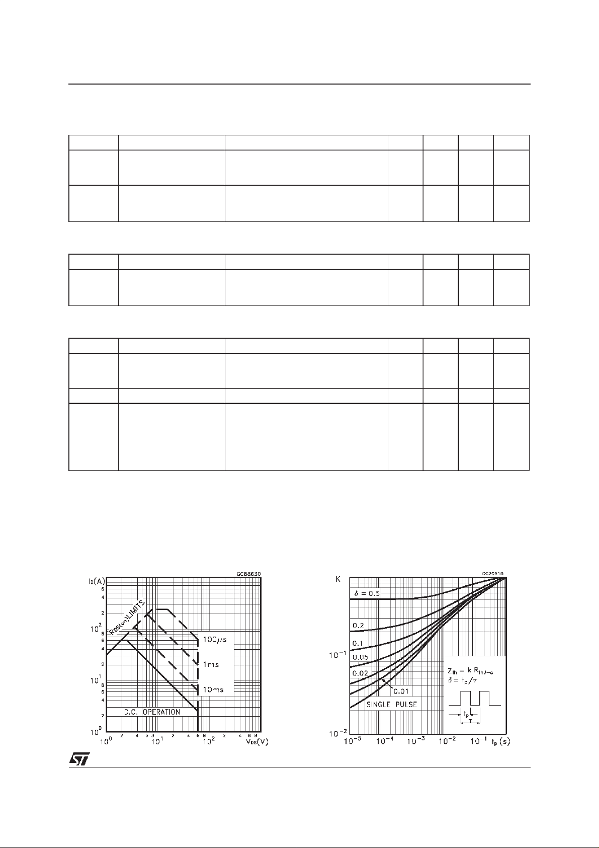
SafeOperating Area ThermalImpedance
3/8
Page 4

STB60NE06L-16
OutputCharacteristics
Transconductance
TransferCharacteristics
Static Drain-sourceOn Resistance
Gate Charge vs Gate-sourceVoltage
4/8
CapacitanceVariations
Page 5

STB60NE06L-16
NormalizedGate ThresholdVoltage vs
Temperature
Source-drainDiode Forward Characteristics
NormalizedOn Resistancevs Temperature
5/8
Page 6

STB60NE06L-16
Fig. 1:
UnclampedInductiveLoad TestCircuit
Fig. 3: SwitchingTimes Test Circuits For
ResistiveLoad
Fig. 2:
UnclampedInductiveWaveform
Fig. 4: Gate Charge test Circuit
Fig. 5:
Test CircuitFor InductiveLoad Switching
And Diode Recovery Times
6/8
Page 7

TO-263 (D2PAK) MECHANICAL DATA
STB60NE06L-16
DIM.
MIN. TYP. MAX. MIN. TYP. MAX.
A 4.4 4.6 0.173 0.181
A1 2.49 2.69 0.098 0.106
B 0.7 0.93 0.027 0.036
B2 1.14 1.7 0.044 0.067
C 0.45 0.6 0.017 0.023
C2 1.21 1.36 0.047 0.053
D 8.95 9.35 0.352 0.368
E 10 10.4 0.393 0.409
G 4.88 5.28 0.192 0.208
L 15 15.85 0.590 0.624
L2 1.27 1.4 0.050 0.055
L3 1.4 1.75 0.055 0.068
mm inch
D
A
C2
DETAIL”A”
C
A2
DETAIL”A”
A1
B2
E
L2
L
L3
B
G
P011P6/E
7/8
Page 8

STB60NE06L-16
Information furnished is believed to be accurate and reliable. However, STMicroelectronics assumes no responsibility for the consequences
of use of such information nor for any infringement of patents or other rights of third parties which may result from its use. No license is
granted by implication or otherwise under any patent or patent rights of STMicroelectronics. Specification mentioned in thispublication are
subject to change withoutnotice. Thispublication supersedes and replaces allinformation previously supplied. STMicroelectronics products
are not authorized for use as critical components in life support devices or systems without express written approval ofSTMicroelectronics.
The ST logo is a trademark of STMicroelectronics
2000 STMicroelectronics – Printedin Italy –All Rights Reserved
STMicroelectronics GROUP OF COMPANIES
Australia - Brazil -China - Finland- France- Germany -Hong Kong - India- Italy- Japan - Malaysia- Malta -Morocco -
Singapore - Spain - Sweden -Switzerland - United Kingdom - U.S.A.
http://www.st.com
8/8
 Loading...