

Page 1
STB60NE06-16
N - CHANNEL ENHANCEMENT MODE
” SINGLE FEATURE SIZE ” POWER MOSFET
TYPE V
DSS
R
DS(on)
I
D
ST B60NE 06-1 60 V < 0.016 Ω 60 A
■ TYPICALR
■ EXCEPTIONALdV/dt CAPABILTY
■ 100% AVALANCHETESTED
■ LOW GATE CHARGE 100
■ HIGH dV/dt CAPABILITY
■ APPLICATIONORIENTED
DS(on)
=0.013 Ω
o
C
CHARACTERIZATION
■ FOR THROUGH-HOLE VERSIONCONTACT
SALESOFFICE
DESCRIPTION
This Power Mosfet is the latest development of
SGS-THOMSONunique ” Single FeatureSize”
strip-based process. The resulting transistor
shows extremelyhigh packing density for low onresistance, rugged avalanche characteristics and
less critical alignment steps therefore a remarkable manufacturingreproducibility.
APPLICATIONS
■ DC MOTOR CONTROL
■ DC-DC& DC-AC CONVERTERS
■ SYNCHRONOUSRECTIFICATION
3
1
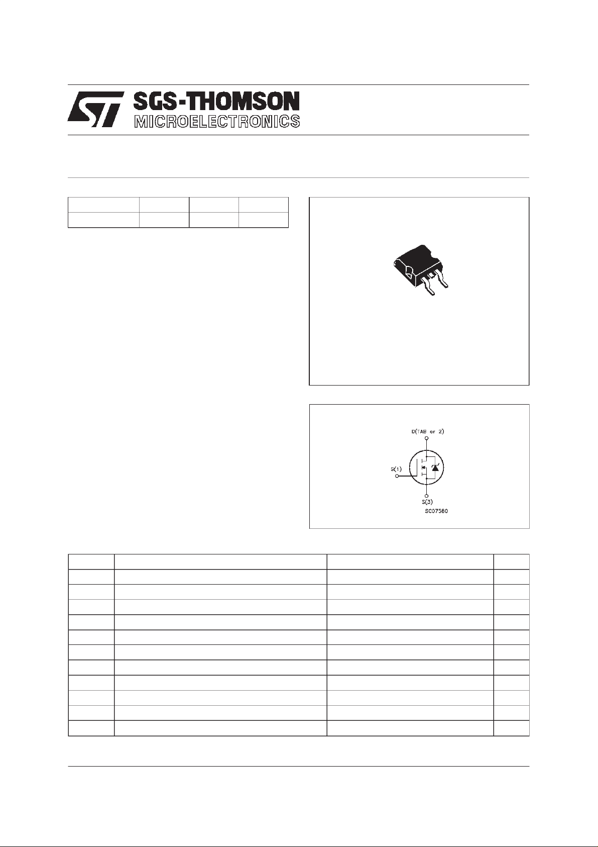
D2PAK
TO-263
(Suffix”T4”)
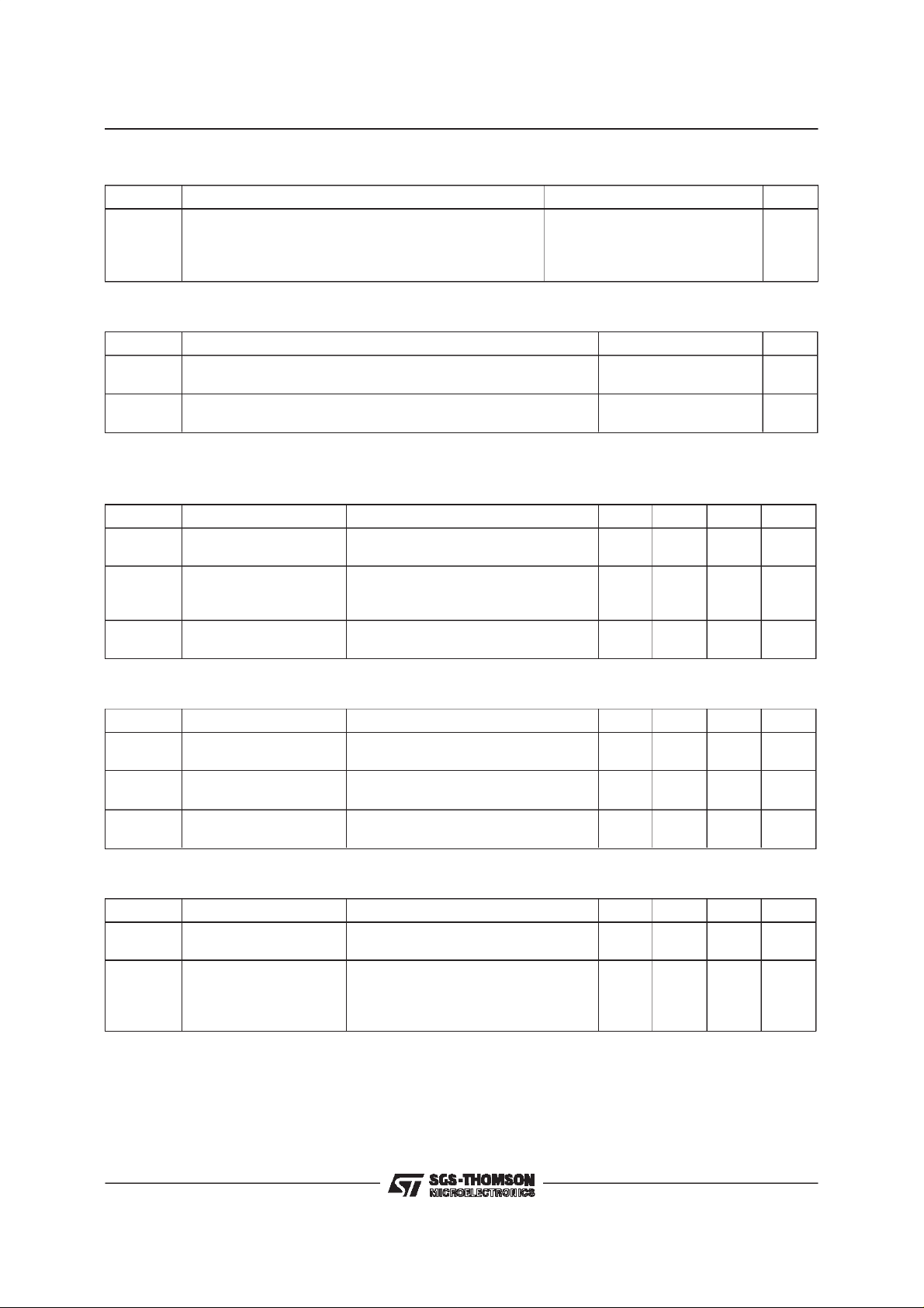
INTERNAL SCHEMATIC DIAGRAM
ABSOLUTE MAXIMUM RATINGS
Symbol Parameter Value Unit
V
V
DGR
V
I
DM
P
dV/ dt(
T
(•) Pulsewidth limitedby safe operatingarea (1)ISD≤ 60 A,di/dt ≤ 200 A/µs, VDD
January 1998
Drain-s ou r ce V olt ag e (VGS=0) 60 V
DS
Drain- gate Voltag e (RGS=20kΩ)
Gate-source Voltage ± 20 V
GS
I
Drain Curren t (cont inu ous) at Tc=25oC60A
D
I
Drain Curren t (cont inu ous) at Tc=100oC42A
D
60 V
(•) Drain Curren t (pulsed) 240 A
Tot al Di s sipa t ion at Tc=25oC 150 W
tot
Derating Factor 1 W/
1) Pea k Diode Recovery vo lta ge slope 6 V/ns
Storage Temperature -65 to 175
stg
T
Max. Operat ing Junct ion Tempe rature 175
j
≤ V
(BR)DSS,TJ
≤
T
JMAX
o
C
o
C
o
C
1/9
Page 2
STB60NE06-16
THERMAL DATA
R
thj-case
Rthj-amb
R
thc-sin k
T
Ther mal Resist ance Junctio n- case Max
Ther mal Resist ance Junctio n- ambient Max
Ther mal Resist ance Case-si nk Ty p
Maximum Lead T e mpera t ure For Sold eri ng P urp os e
l
1
62.5
0.5
300
AVALANCHE CHARACTERISTICS
Symbol Para met e r Max Valu e Unit
I
AR
E
Avalanch e Curre nt , Repet it i v e or Not - Re petit ive
(pulse w idth limited by T
Single Pulse Avalanche Energy
AS
(starting T
=25oC, ID=IAR,VDD=25V)
j
max, δ <1%)
j
ELECTRICAL CHARACTERISTICS (T
=25oC unlessotherwisespecified)
case
60 A
350 mJ
OFF
Symbol Parameter Test Cond ition s Min. Typ. Max. Unit
V
(BR)DSS
I
DSS
I
GSS
Drain-sou rc e
Breakdown Voltage
Zer o Gate Vo lt age
Drain Cur rent (V
GS
Gat e-body Leaka ge
Current (V
DS
=0)
=0)
=250µAVGS=0
I
D
V
=MaxRating
DS
=MaxRating Tc=125
V
DS
o
C
= ± 20 V
V
GS
60 V
1
10
± 100 nA
o
C/W
o
C/W
oC/W
o
C
µA
µA
ON (∗)
Symbol Parameter Test Cond ition s Min. Typ. Max. Unit
V
GS(th )
Gate Threshold
V
DS=VGSID
=250µA
234V
Voltage
R
DS(on)
Stati c Drain-so urce On
VGS=10V ID= 30 A 0.013 0.016 Ω
Resistance
I
D(on)
On Stat e Drain Cur rent VDS>I
D(on)xRDS(on)max
60 A
VGS=10V
DYNAMIC
Symbol Parameter Test Cond ition s Min. Typ. Max. Unit
g
(∗)Forward
fs
Tr anscond uctanc e
C
C
C
Input Capaci t an ce
iss
Out put C apa citance
oss
Reverse Transfer
rss
Capa cit an c e
VDS>I
D(on)xRDS(on)maxID
=30 A 20 35 S
VDS=25V f=1MHz VGS= 0 4600
580
140
6200
800
200
pF
pF
pF
2/9
Page 3
STB60NE06-16
ELECTRICAL CHARACTERISTICS (continued)
SWITCHINGON
Symbol Parameter Test Cond ition s Min. Typ. Max. Unit
t
d(on)
(di/dt)
Q
Q
Q
Turn-on Time
Rise Time
t
r
Turn-on Current Slope VDD=48V ID=60A
on
Total Gate Charge
g
Gat e-Sou r ce Charge
gs
Gate-Drain Charge
gd
VDD=30V ID=30A
=4.7 Ω VGS=10V
R
G
=47 Ω VGS=10 V
R
G
VDD=48V ID=60A VGS= 10 V 115
SWITCHINGOFF
Symbol Parameter Test Cond ition s Min. Typ. Max. Unit
t
r(Voff)
t
Of f - voltag e Rise T ime
t
Fall Time
f
Cross-over Time
c
VDD=48V ID=60A
=4.7 Ω VGS=10V
R
G
SOURCE DRAIN DIODE
Symbol Parameter Test Cond ition s Min. Typ. Max. Unit
I
SD
I
SDM
V
SD
t
Q
I
RRM
(∗) Pulsed: Pulse duration =300 µs, duty cycle1.5 %
(•) Pulse widthlimited by safe operating area
Source-drain Current
(•)
Source-drain Current
(pulsed)
(∗) For ward On Voltage ISD=60A VGS=0 1.5 V
Reverse Recov ery
rr
Time
Reverse Recov ery
rr
= 60 A di/dt = 10 0 A/µs
I
SD
=30V Tj=150oC
V
DD
Charge
Reverse Recov ery
Current
40
12560180
280 A/ µs
160 nC
25
40
15
150
180
25
210
260
60
240
100
0.4
8
ns
ns
nC
nC
ns
ns
ns
A
A
ns
µC
A
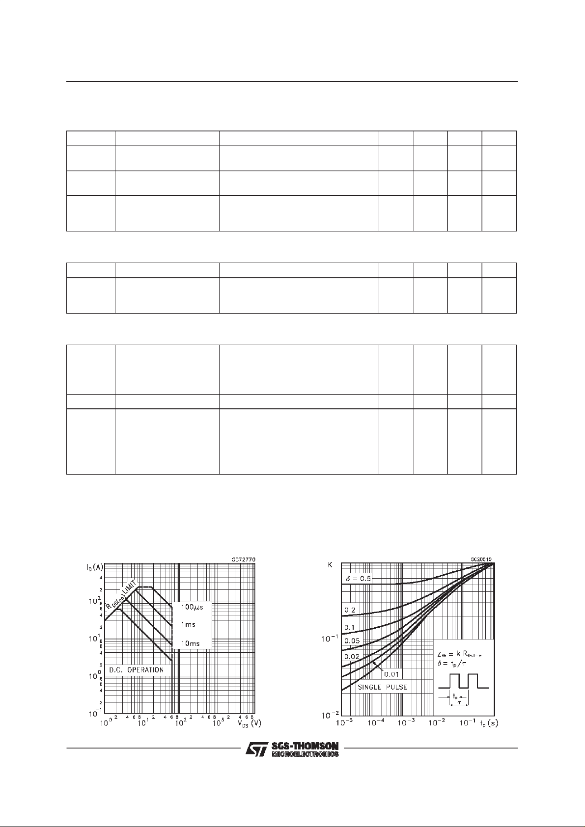
Safe Operating Area ThermalImpedance
3/9
Page 4

STB60NE06-16
Derating Curve
TransferCharacteristics
OutputCharacteristics
Transconductance
StaticDrain-source On Resistance
4/9
Gate Charge vsGate-sourceVoltage
Page 5

STB60NE06-16
CapacitanceVariations
Normalized OnResistance vsTemperature
Normalized Gate ThresholdVoltagevs
Temperature
Turn-onCurrent Slope
Turn-offDrain-source VoltageSlope
Cross-overTime
5/9
Page 6

STB60NE06-16
SwitchingSafe OperatingArea
Source-drainDiode Forward Characteristics
AccidentalOverloadArea
Fig. 1: UnclampedInductiveLoad TestCircuit
6/9
Fig. 2: UnclampedInductiveWaveform
Page 7

STB60NE06-16
Fig. 3: Switching Times Test CircuitsFor
ResistiveLoad
Fig. 5: Test CircuitFor InductiveLoad Switching
And DIodeRecovery Times
Fig. 4: Gate Chargetest Circuit
7/9
Page 8

STB60NE06-16
TO-263 (D2PAK) MECHANICAL DATA
DIM.
MIN. TYP. MAX. MIN. TYP. MAX.
A 4.3 4.6 0.169 0.181
A1 2.49 2.69 0.098 0.106
B 0.7 0.93 0.027 0.036
B2 1.25 1.4 0.049 0.055
C 0.45 0.6 0.017 0.023
C2 1.21 1.36 0.047 0.053
D 8.95 9.35 0.352 0.368
E 10 10.28 0.393 0.404
G 4.88 5.28 0.192 0.208
L 15 15.85 0.590 0.624
L2 1.27 1.4 0.050 0.055
L3 1.4 1.75 0.055 0.068
mm inch
E
A
C2
L2
D
L
L3
B2
B
A1
C
G
P011P6/C
8/9
Page 9

STB60NE06-16
Information furnished is believed to be accurateand reliable. However, SGS-THOMSONMicroelectronics assumes no responsability for the
consequencesof use ofsuch information nor for any infringement of patentsor other rights of third parties whichmay resultsfrom its use. No
licenseisgrantedby implicationor otherwise underany patentorpatent rightsofSGS-THOMSONMicroelectronics.Specifications mentioned
in this publicationare subjectto change without notice.This publicationsupersedes and replaces all informationpreviouslysupplied.
SGS-THOMSONMicroelectronics products are notauthorizedforuseas criticalcomponents in lifesupportdevices or systemswithoutexpress
writtenapproval of SGS-THOMSONMicroelectonics.
1997 SGS-THOMSONMicroelectronics- Printedin Italy- AllRights Reserved
Australia- Brazil - Canada- China- France-Germany- Italy- Japan - Korea -Malaysia- Malta- Morocco - The Netherlands -
Singapore- Spain- Sweden- Switzerland- Taiwan - Thailand - United Kingdom- U.S.A
SGS-THOMSONMicroelectronics GROUPOF COMPANIES
...
9/9
 Loading...