

Page 1
STP5NC50 - STP5NC50FP
STB5NC50 - STB5NC50-1
N-CHANNEL 500V - 1.3Ω - 5.5A T O-220/FP/D2PAK/I2PAK
PowerMesh™II MOSFET
TYPE V
STP5NC50
STP5NC50FP
STB5NC50
STB5NC50-1
■ TYPICAL R
■ EXTREMELY HIGH dv/dt CAPABILITY
■ 100% A V ALANCHE TESTED
■ NEW HIGH VOLTAGE BENCHMARK
■ GATE CHARGE MINIMIZED
DS
DSS
500 V
500 V
500 V
500 V
(on) = 1.3Ω
R
DS(on)
<1.5Ω
<1.5Ω
<1.5Ω
<1.5Ω
I
D
5.5A
5.5A
5.5A
5.5A
DESCRIPTION
The PowerMESH
generation of MESH OV ERLAY
™II is the evolution of the first
™. T he layout re-
finements introduced greatly improv e the Ron*area
figure of merit while keeping the device at the leading edge for what concerns swithing s peed, gate
charge and ruggedness.
APPLICATIONS
■ HIGH CURRENT, HIGH SPEED SWITCHING
■ SWITH MODE POWER SUPPLIES (SMPS)
■ DC-AC CONVERTERS FOR WELDING
EQUIPMENT AND UNINTERRUPTIBLE
POWER SUPPLIES AND MOTOR DRIVES
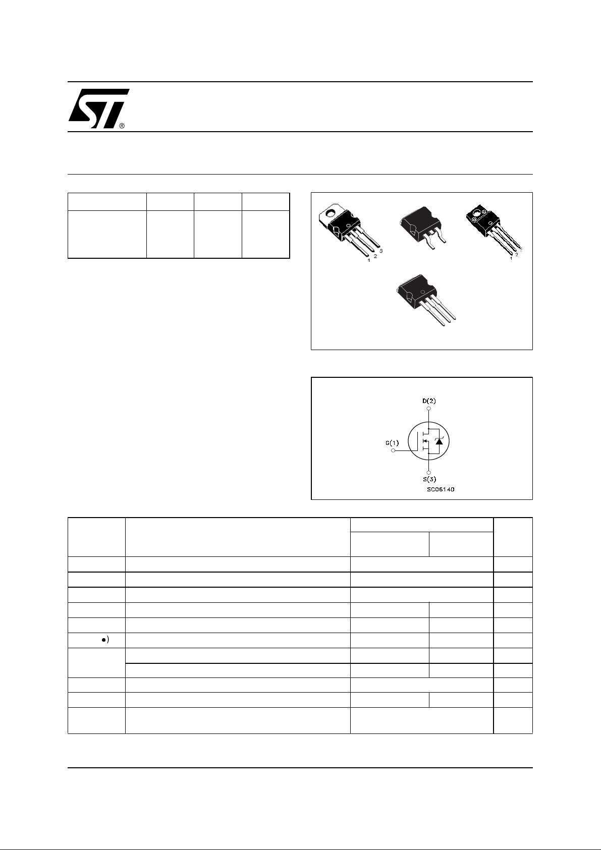
3
1
TO-220
D2PAK
3
2
1
TO-220FP
I2PAK
INTERNAL SCHEM ATIC DIAGRAM
ABSOLUTE MAXIMUM RATINGS
Symbol Parameter Value Unit
STP5NC50
STB5NC50/-1
Drain-source Voltage (VGS=0)
Drain-gate Voltage (RGS=20kΩ)
Gate- source Voltage ±30 V
Drain Current (continuos) at TC= 25°C
Drain Current (continuos) at TC= 100°C
()
Drain Current (pulsed) 22 22 A
Total Dissipation at TC= 25°C
5.5 5.5(*) A
3.5 3.5(*) A
100 35 W
I
V
DM
P
V
DGR
V
I
I
TOT
DS
GS
D
D
Derating Factor 0.8 0.28 W/°C
dv/dt(1) Peak Diode Recovery voltage slope 3.5 V/ns
V
ISO
T
T
stg
(•)Pulse width limited by safe operating area
≤5.5A, di/dt ≤100A/µs, VDD≤ V
(1)I
SD
Insulation Withstand Voltage (DC) - 2500 V
Operating Junction Temperature
j
Storage Temperature
(*)Limited only by maximum temperature allowed
(BR)DSS,Tj≤TJMAX.
-55 to 175
-65 to 175
STP5NC50FP
500 V
500 V
°C
°C
1/12December 2002
Page 2
STP5NC50 - ST P5NC 50FP - STB5N C50 - STB5NC50-1
THERMAL DATA
TO-220
2
D
PAK
2
PAK
I
Rthj-case Thermal Resistance Junction-case Max 1.25 3.57 °C/W
Rthj-amb Thermal Resistance Junction-ambient Max 62.5 °C/W
T
Maximum Lead Temperature For Soldering Purpose 300 °C
l
AVALANCHE CHARACTERISTICS
Symbol Parameter Max Value Unit
I
AR
E
AS
Avalanche Current, Repetitive or Not-Repetitive
(pulse width limited by T
max)
j
Single Pulse Avalanche Energy
(starting T
= 25 °C, ID=IAR,VDD=50V)
j
ELECTRICAL CHARACTERISTICS (TCASE = 25 °C UNLESS OTHE RWIS E SPECIFIED)
OFF
Symbol Parameter Test Conditions Min. Typ. Max. Unit
V
(BR)DSS
I
DSS
I
GSS
Drain-source
Breakdown Voltage
Zero Gate Voltage
Drain Current (V
GS
Gate-body Leakage
Current (V
DS
=0)
=0)
ID= 250µA, VGS= 0 500 V
V
= Max Rating
DS
= Max Rating, TC= 125 °C
V
DS
V
= ±30V ±100 nA
GS
TO-220FP
5.5 A
280 mJ
1µA
50 µA
(1)
ON
Symbol Parameter Test Conditions Min. Typ. Max. Unit
V
GS(th)
R
DS(on)
Gate Threshold Voltage
Static Drain-source On
V
DS=VGS,ID
VGS=10V,ID=2A
= 250µA
234V
1.3 1.5 Ω
Resistance
DYNAMIC
Symbol Parameter Test Conditions Min. Typ. Max. Unit
(1)
g
fs
C
iss
C
oss
C
rss
Forward Transconductance VDS>I
Input Capacitance
Output Capacitance 80 pF
Reverse Transfer
Capacitance
D(on)xRDS(on)max,
ID= 2.5A
V
=25V,f=1MHz,VGS=0
DS
4S
480 pF
11.5 pF
2/12
Page 3
STP5NC50 - STP5NC50FP - STB5NC50 - STB5NC50-1
ELECTRICAL CHARACTERISTICS
(CONTINUED)
SWITCHING ON
Symbol Parameter Test Conditions Min. Typ. Max. Unit
V
t
d(on)
t
r
Q
Q
gs
Q
gd
Turn-on Delay Time
Rise Time
Total Gate Charge
g
Gate-Source Charge 3 nC
Gate-Drain Charge 9 nC
SWITCHING OFF
Symbol Parameter Test Conditions Min. Typ. Max. Unit
t
r(Voff)
t
t
f
c
Off-voltage Rise Time
Fall Time 14 ns
Cross-over Time 20 ns
SOURCE DR AIN DIODE
Symbol Parameter Test Conditions Min. Typ. Max. Unit
I
SD
I
SDM
V
SD
t
rr
Q
rr
I
RRM
Note: 1. Pulsed:Pulseduration=300µs,dutycycle1.5%.
2. Pulse width limited by safeoperating area.
Source-drain Current 5.5 A
(2)
Source-drain Current (pulsed) 22 A
(1)
Forward On Voltage
Reverse Recovery Time
Reverse Recovery Charge 1.6 µC
Reverse Recovery Current 9 A
=250V,ID= 2.5A
DD
R
= 4.7Ω VGS=10V
G
(see test circuit, Figure 3)
V
=400V,ID= 5.5A,
DD
=10V
V
GS
V
= 400V, ID= 5.5A,
DD
RG=4.7Ω, VGS= 10V
(see test circuit, Figure 5)
ISD= 5.5A, VGS=0
I
= 5.5A, di/dt = 100A/µs,
SD
VDD=100V,Tj=150°C
(see test circuit, Figure 5)
14 ns
15 ns
17.5 24.5 nC
12 ns
1.6 V
360 ns
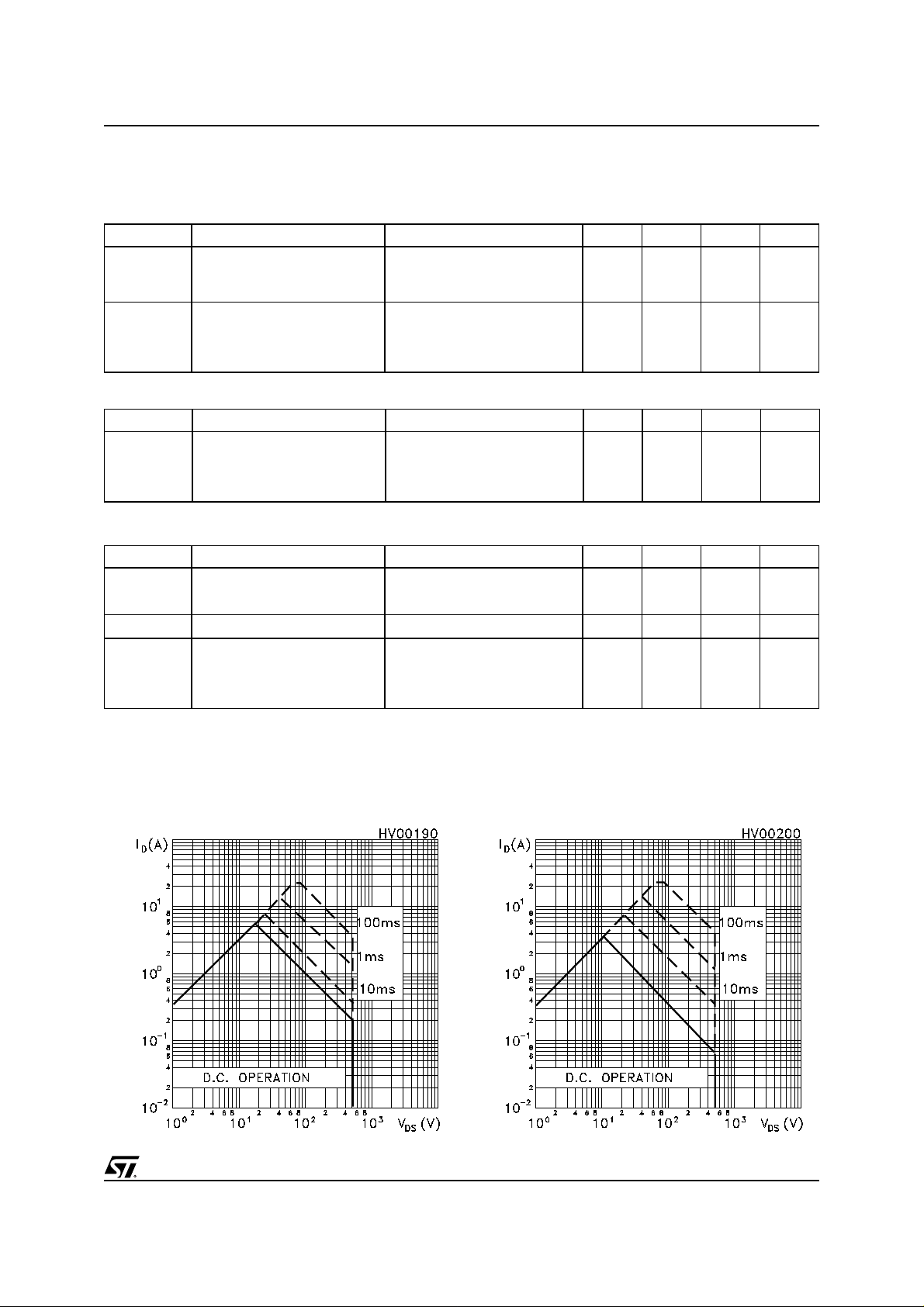
Safe Operating Area for TO-220FPSafe Operating Area for TO-220/D2PAK/I2PAK
3/12
Page 4
STP5NC50 - ST P5NC 50FP - STB5N C50 - STB5NC50-1
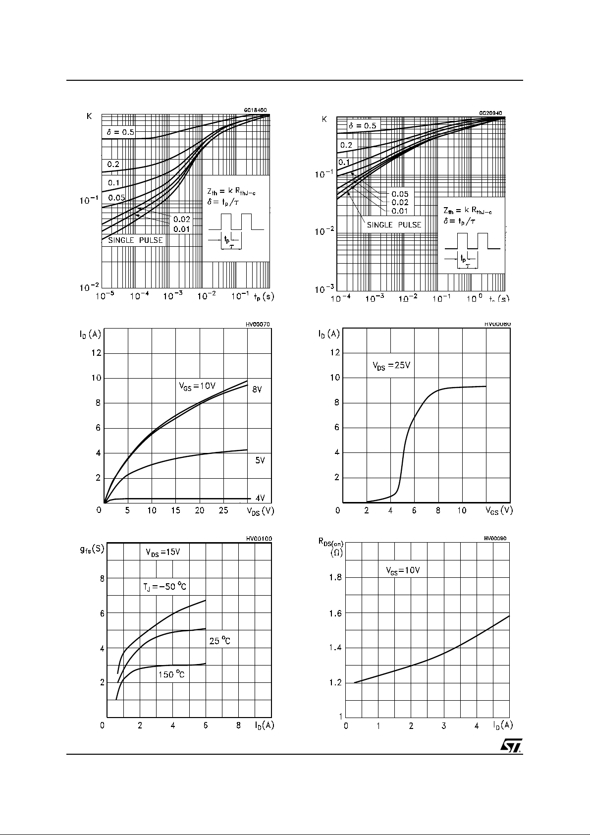
Thermal Impedence for TO-220/D2PAK/I2PAK
Output Characteristics
Thermal Impedence for TO-220FP
Transfer Characteristics
Transconductance Static D rain-source On Resistance
4/12
Page 5

STP5NC50 - STP5NC50FP - STB5NC50 - STB5NC50-1
Gate Char ge vs Gate-sourc e Voltage Capacitance Variations
Normalized Gate Threshold Voltage vs Temp.
Source-drain Diode Forward Characteristics
Normalized On Resistance vs Temperature
5/12
Page 6

STP5NC50 - ST P5NC 50FP - STB5N C50 - STB5NC50-1
Fig. 2: Unclamped Inductive WaveformFig. 1: Unclamped Inductive Load Test Circuit
Fig. 3: Switching Times Test Circuit For
Resistive Load
Fig. 5: Test Circuit For Inductive Load Switching
And Diode Recovery T imes
Fig. 4: Gate Charge test Circuit
6/12
Page 7

STP5NC50 - STP5NC50FP - STB5NC50 - STB5NC50-1
E
P011C
TO-220 MECHANICAL DATA
DIM.
A 4.40 4.60 0.173 0.181
C 1.23 1.32 0.048 0.051
D 2.40 2.72 0.094 0.107
D1 1.27 0.050
E 0.49 0.70 0.019 0.027
F 0.61 0.88 0.024 0.034
F1 1.14 1.70 0.044 0.067
F2 1.14 1.70 0.044 0.067
G 4.95 5.15 0.194 0.203
G1 2.4 2.7 0.094 0.106
H2 10.0 10.40 0.393 0.409
L2 16.4 0.645
L4 13.0 14.0 0.511 0.551
L5 2.65 2.95 0.104 0.116
L6 15.25 15.75 0.600 0.620
L7 6.2 6.6 0.244 0.260
L9 3.5 3.93 0.137 0.154
DIA. 3.75 3.85 0.147 0.151
MIN. TYP. MAX. MIN. TYP. MAX.
mm inch
A
C
D
L5
Dia.
L7
D1
L6
L2
L9
F1
G1
F
H2
G
F2
L4
7/12
Page 8

STP5NC50 - ST P5NC 50FP - STB5N C50 - STB5NC50-1
TO-220FP MECHANICAL DATA
DIM.
A 4.4 4.6 0.173 0.181
B 2.5 2.7 0.098 0.106
D 2.5 2.75 0.098 0.108
E 0.45 0.7 0.017 0.027
F 0.75 1 0.030 0.039
F1 1.15 1.5 0.045 0.067
F2 1.15 1.5 0.045 0.067
G 4.95 5.2 0.195 0.204
G1 2.4 2.7 0.094 0.106
H 10 10.4 0.393 0.409
L2 16 0.630
L3 28.6 30.6 1.126 1.204
L4 9.8 10.6 0.385 0.417
L5 2.9 3.6 0.114 0.141
L6 15.9 16.4 0.626 0.645
L7 9 9.3 0.354 0.366
Ø 3 3.2 0.118 0.126
MIN. TYP MAX. MIN. TYP. MAX.
mm. inch
E
A
D
B
L3
L6
L7
¯
F1
F
G1
H
G
F2
123
L2
L5
L4
8/12
Page 9

STP5NC50 - STP5NC50FP - STB5NC50 - STB5NC50-1
D2PAK MECHANICAL DATA
DIM.
MIN. TYP MAX. MIN. TYP. MAX.
A 4.4 4.6 0.173 0.181
A1 2.49 2.69 0.098 0.106
A2 0.03 0.23 0.001 0.009
B 0.7 0.93 0.027 0.036
B2 1.14 1.7 0.044 0.067
C 0.45 0.6 0.017 0.023
C2 1.23 1.36 0.048 0.053
D 8.95 9.35 0.352 0.368
D1 8 0.315
E 10 10.4 0.393
E1 8.5 0.334
G 4.88 5.28 0.192 0.208
L 15 15.85 0.590 0.625
L2 1.27 1.4 0.050 0.055
L3 1.4 1.75 0.055 0.068
mm. inch
M 2.4 3.2 0.094 0.126
R 0.4 0.015
V2 0º 8º
3
9/12
1
Page 10

STP5NC50 - ST P5NC 50FP - STB5N C50 - STB5NC50-1
P011P5/E
TO-262 (I2PAK) MECHANICAL DATA
DIM.
MIN. TYP. MAX. MIN. TYP. MAX.
A 4.4 4.6 0.173 0.181
A1 2.49 2.69 0.098 0.106
B 0.7 0.93 0.027 0.036
B2 1.14 1.7 0.044 0.067
C 0.45 0.6 0.017 0.023
C2 1.23 1.36 0.048 0.053
D 8.95 9.35 0.352 0.368
e 2.4 2.7 0.094 0.106
E 10 10.4 0.393 0.409
L 13.1 13.6 0.515 0.531
L1 3.48 3.78 0.137 0.149
L2 1.27 1.4 0.050 0.055
mm inch
C
A
A1
10/12
C2
B2
B
e
E
L1
L2
D
L
Page 11

STP5NC50 - STP5NC50FP - STB5NC50 - STB5NC50-1
D2PAK FOOTPRINT
TAPE AND REEL SHIPMENT (suffix ”T4”)*
TUBE SHIPMENT (no suffix)*
REEL MECHANICAL DATA
DIM.
A 330 12.992
B 1.5 0.059
C 12.8 13. 2 0.504 0.520
D 20.2 0795
G 24.4 26.4 0.960 1.039
N 100 3.937
T 30.4 1.197
mm inch
MIN. MAX. MIN. MAX.
TAPE MECHANICAL DATA
DIM.
A0 10.5 10.7 0.413 0.421
B0 15.7 15.9 0.618 0.626
D 1.5 1.6 0.059 0 .063
D1 1.59 1.61 0. 062 0.063
E 1. 65 1.85 0.065 0.073
F 11.4 11.6 0.449 0 .456
K0 4. 8 5.0 0.189 0.197
P0 3.9 4.1 0.153 0.161
P1 11.9 12.1 0.468 0.476
P2 1.9 2.1 0.075 0.082
R 50 1.574
T 0.25 0.35 0.0098 0.0137
W 23.7 24.3 0.933 0.956
* on sales type
mm inch
MIN. MAX. MIN. MAX.
BASE QTY BULK QTY
1000 1000
11/12
Page 12

STP5NC50 - ST P5NC 50FP - STB5N C50 - STB5NC50-1
Information furnished is believed to be accurate and reliable. However, STMicroelectronics assumes no responsibility for t he
consequences of use of su ch in formation nor for any in fringement of patents or other rights of third parties w hich may result from
its use. No license is granted by implication or otherwise under any patent or patent rights of STMicroelectronics. Specifications
mentioned in this publication are subject to change without notice. This publication supersedes and replaces all information
previously suppli ed. STMi croelect ronics pr oducts are not author ized for use as cr itical component s in li fe suppo rt devi ces or
systems without express written approval of STMicroelectronics.
Australia - Brazil - Canada - China - Finland - France - Germany - Hong Kong - India - Israel - Italy - Japan - Malaysia - Malta - Morocco
© The ST logo is a registered trademark of STMicroelectronics
© 2002 STMicroelectronics - Printed in Italy - All Rights Reserved
Singapore - Spain - Sweden - Switzerland - United Kingdom - United States.
STMicroelectronics GROUP OF COMPANIES
© http://www.st.com
12/12
 Loading...