

Page 1
STB5NB80
N - CHANNEL 800V - 1.8Ω -5A-D2PAK
PowerMESH MOSFET
TYPE V
DSS
R
DS(on)
I
D
STB5NB80 800 V < 2.2 Ω 5A
■ TYPICALR
■ EXTREMELYHIGH dv/dt CAPABILITY
■ 100%AVALANCHETESTED
■ VERYLOW INTRINSIC CAPACITANCES
■ GATECHARGE MINIMIZED
■ ADDSUFFIX ”T4” FOR ORDERING IN TAPE
DS(on)
= 1.8
Ω
& REEL
DESCRIPTION
Using the latest high voltageMESH OVERLAY
process, STMicroelectronics has designed an
advanced family of power MOSFETs with
outstanding performances. The new patent
pending strip layout coupled with the Company’s
proprietary edge termination structure, gives the
lowest RDS(on) per area, exceptional avalanche
and dv/dt capabilities and unrivalled gate charge
and switching characteristics.
APPLICATIONS
■ HIGHCURRENT, HIGHSPEEDSWITCHING
■ DC-AC CONVERTERS FOR WELDING
■ EQUIPMENTAND UNINTERRUPTIBLE
POWERSUPPLIESAND MOTORDRIVE
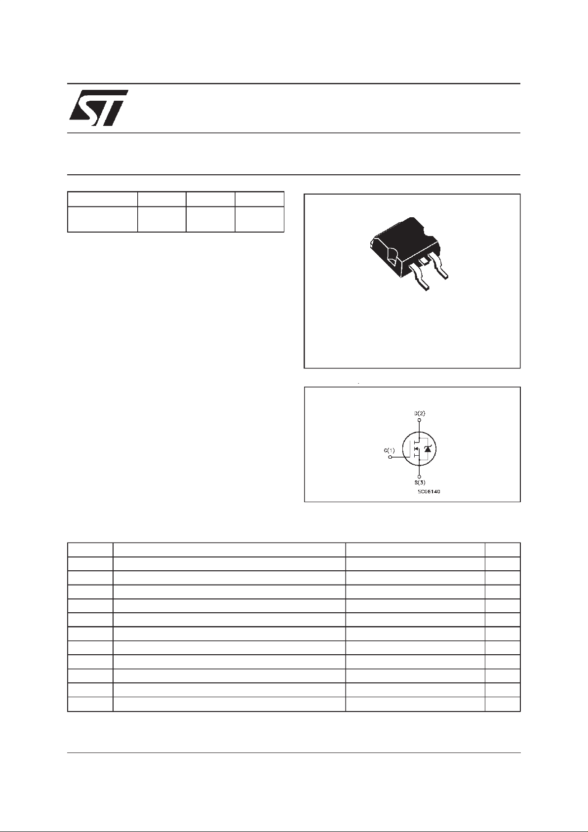
3
1
D2PAK
TO-263
INTERNAL SCHEMATIC DIAGRAM
ABSOLUTE MAXIMUM RATINGS
Symbol Parameter Value Unit
V
V
V
I
DM
P
dv/ dt(
T
(*) Limited only by maximum temperature allowed (1)ISD≤ 5A, di/dt ≤ 200 A/µs,VDD≤ V
March 1999
Drain-source Voltage (VGS=0) 800 V
DS
Dra in- gat e Voltage (RGS=20kΩ)
DGR
Gate -source Voltage
GS
I
Dra in Cur ren t (continuous ) a t Tc=25oC5A
D
I
Dra in Cur ren t (continuous ) a t Tc= 100oC3.2A
D
800 V
30 V
±
(•) Dra in Curr en t (puls ed) 20 A
Tot al Dissipati on at Tc=25oC110W
tot
Der at ing Factor 0.88 W/
1) Peak Diode Recovery voltag e slope 4 V / ns
St orage Tem pe ra t ure -65 to 150
stg
T
Max. Op erat i ng J unction Temperature 150
j
,Tj≤T
(BR)DSS
JMAX
o
C
o
C
o
C
1/8
Page 2

STB5NB80
THERMAL DATA
R
thj-case
R
thj-amb
R
thc-sink
T
AVALANCHE CHARACTERISTICS
Ther mal Resis t an ce Junc ti on-cas e Max 1.13
Ther mal Resis t an ce Junc ti on-ambien t Max
Thermal Resistance Case-sink Typ
Maximum Lead Tem per at ure For S old er ing Pur p ose
l
62.5
0.5
300
o
C/W
o
C/W
o
C/W
o
C
Symbol Para meter Mi n .
I
AR
E
ELECTRICAL CHARACTERISTICS
Avalanche Curr ent, Repet itiv e or Not-Repetitive
(pulse width limited by T
Single Pu lse Avalanche En ergy
AS
(starting T
=25oC, ID=IAR,VDD=50V)
j
max)
j
(T
case
=25oC unless otherwisespecified)
Value
Max.
Value
5A
300 mJ
OFF
Symbol Parameter Test Conditions Min. Typ. Max. Unit
V
(BR)DSS
Drain-sourc e
=250µAVGS=0
I
D
800 V
Break d own Voltage
I
DSS
I
GSS
Zero Gate Voltage
Drain Cu rr ent (V
GS
Gat e- b ody Leak a ge
Current (V
DS
=0)
=0)
V
=MaxRating
DS
= Max Rating Tc=125oC
V
DS
=± 30 V
V
GS
1
50
100 nA
±
ON(∗)
Symbol Parameter Test Conditions Min. Typ. Max. Unit
V
GS(th)
R
DS(on)
I
D(on)
Gate Threshold
V
DS=VGSID
Voltage
Static Drain-source O n
VGS=10V ID= 2.5 A 1.8 2.2 Ω
Resistanc e
On Stat e Dra in Curr ent VDS>I
VGS=10V
= 250µA
D(on)xRDS(on)max
345V
5A
Unit
A
µ
µA
DYNAMIC
Symbol Parameter Test Conditions Min. Typ. Max. Unit
g
(∗)Forward
fs
C
iss
C
oss
C
rss
2/8
Tr ansconduc tance
Input Cap acitan ce
Out put Capac it ance
Reverse Transfer
Capacitance
VDS>I
D(on)xRDS(on)maxID
=2.5A 1.5 4 S
VDS=25V f=1MHz VGS= 0 1050
135
15
pF
pF
pF
Page 3
STB5NB80
ELECTRICAL CHARACTERISTICS
(continued)
SWITCHING ON
Symbol Parameter Test Conditions Min. Typ. Max. Unit
t
d(on)
Turn-on delay Time
t
Rise Time
r
VDD= 400 V ID=3A
=4.7 Ω VGS=10V
R
G
18
9
(see t est circuit, figure 3)
Q
Q
Q
Total Gate Charge
g
Gat e- Source Char ge
gs
Gate-Drain Charge
gd
VDD= 480 V ID=5.6A VGS=10V 30
9
14
42 nC
SWITCHING OFF
Symbol Parameter Test Conditions Min. Typ. Max. Unit
t
r(Voff)
t
t
Off -voltage R ise T ime
Fall Time
f
Cross-ov er Ti m e
c
VDD= 640 V ID=5.6A
=4.7 Ω VGS=10V
R
G
(see t est circuit, figure 5)
14
14
21
SOURCEDRAINDIODE
Symbol Parameter Test Conditions Min. Typ. Max. Unit
I
SD
I
SDM
V
SD
t
Q
I
RRM
(∗) Pulsed: Pulse duration = 300 µs, duty cycle 1.5 %
(•) Pulse width limited by safe operatingarea
Source-drain Curr ent
(•)
Source-drain Curr ent
5
20
(pulsed)
(∗) F orwar d On Voltage ISD=5A VGS=0 1.6 V
Reverse Recov ery
rr
Time
Reverse Recov ery
rr
=5.6A di/dt=100A/µs
I
SD
= 100 V Tj=150oC
V
DD
(see t est circuit, figure 5)
700
5
Charge
Reverse Recov ery
14
Current
ns
ns
nC
nC
ns
ns
ns
A
A
ns
µ
A
C
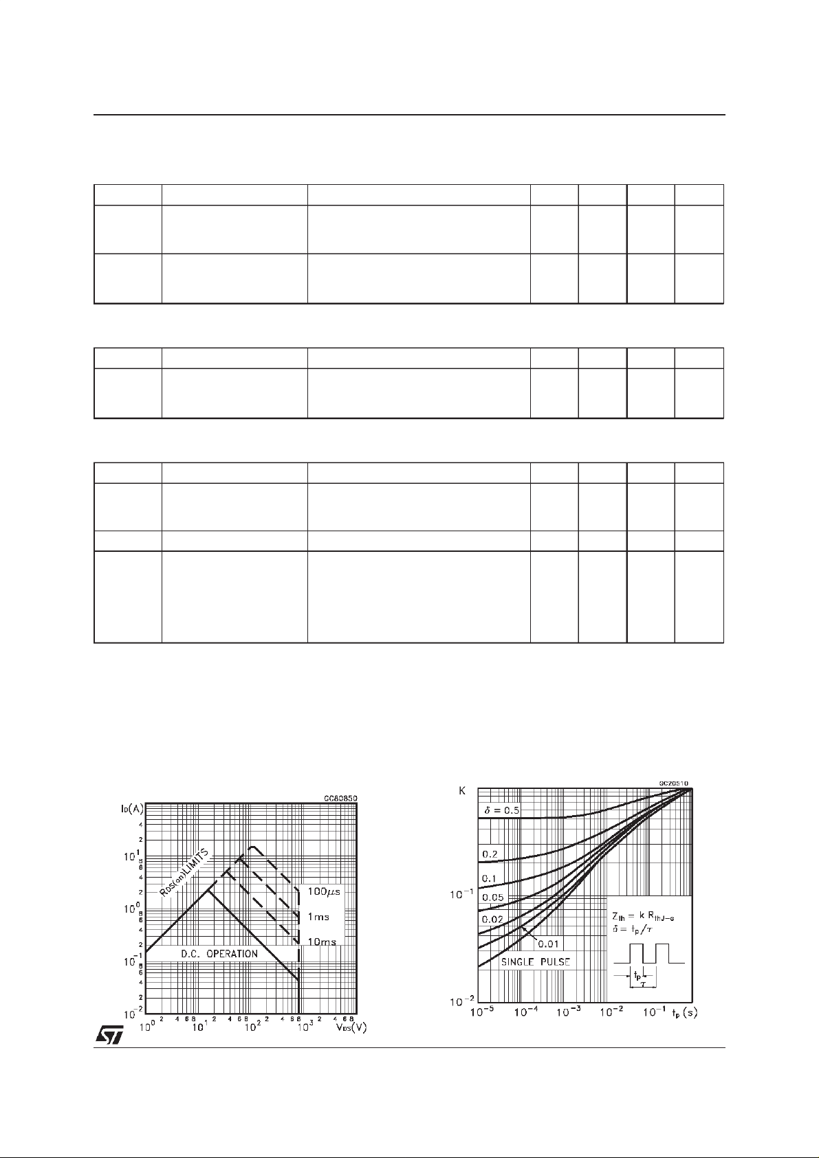
SafeOperating Area Thermal Impedance
3/8
Page 4

STB5NB80
OutputCharacteristics
Transconductance
TransferCharacteristics
Static Drain-sourceOn Resistance
Gate Charge vs Gate-sourceVoltage
4/8
CapacitanceVariations
Page 5

STB5NB80
Normalized GateThresholdVoltage vs
Temperature
Source-drainDiode Forward Characteristics
Normalized On Resistance vsTemperature
5/8
Page 6

STB5NB80
Fig. 1: Unclamped InductiveLoad Test Circuit
Fig. 3: Switching Times Test CircuitsFor
ResistiveLoad
Fig. 2: Unclamped InductiveWaveform
Fig. 4: Gate Chargetest Circuit
Fig. 5: Test Circuit For InductiveLoad Switching
And Diode Recovery Times
6/8
Page 7

TO-263 (D2PAK) MECHANICAL DATA
STB5NB80
DIM.
MIN. TYP. MAX. MIN. TYP. MAX.
A 4.3 4.6 0.169 0.181
A1 2.49 2.69 0.098 0.106
B 0.7 0.93 0.027 0.036
B2 1.25 1.4 0.049 0.055
C 0.45 0.6 0.017 0.023
C2 1.21 1.36 0.047 0.053
D 8.95 9.35 0.352 0.368
E 10 10.28 0.393 0.404
G 4.88 5.28 0.192 0.208
L 15 15.85 0.590 0.624
L2 1.27 1.4 0.050 0.055
L3 1.4 1.75 0.055 0.068
mm inch
E
A
C2
L2
D
L
L3
B2
B
A1
C
G
P011P6/C
7/8
Page 8

STB5NB80
Information furnishedis believedto beaccurate and reliable.However, STMicroelectronics assumesno responsibility for the consequences
of use of such information nor for any infringement of patents or other rights of third parties which may result from its use. No license is
granted by implication or otherwise under any patent or patent rights of STMicroelectronics. Specificationmentioned in this publication are
subjecttochange without notice. This publicationsupersedesandreplaces all information previouslysupplied. STMicroelectronicsproducts
are not authorized for use as critical components in life support devicesor systemswithout express written approval of STMicroelectronics.
The STlogo is atrademark of STMicroelectronics
1999 STMicroelectronics – Printed in Italy – All Rights Reserved
STMicroelectronics GROUP OF COMPANIES
Australia - Brazil - Canada -China - France - Germany - Italy - Japan - Korea - Malaysia - Malta - Mexico - Morocco - The Netherlands -
8/8
Singapore - Spain - Sweden - Switzerland - Taiwan - Thailand - United Kingdom - U.S.A.
http://www.st.com
.
 Loading...