

Page 1
N - CHANNEL ENHANCEMENT MODE
TYPE V
DSS
STB5NA80 800 V < 2.4 Ω 4.7 A
R
DS(on)
I
D
STB5NA80
POWER MOS TRANSISTOR
PRELIMINARY DATA
■ TYPICALR
■ AVALANCHERUGGEDTECHNOLOGY
■ 100% AVALANCHETESTED
■ REPETITIVEAVALANCHEDATAAT 100
■ LOW GATE CHARGE
■ VERYHIGH CURRENT CAPABILITY
■ APPLICATIONORIENTED
DS(on)
=1.8 Ω
o
C
CHARACTERIZATION
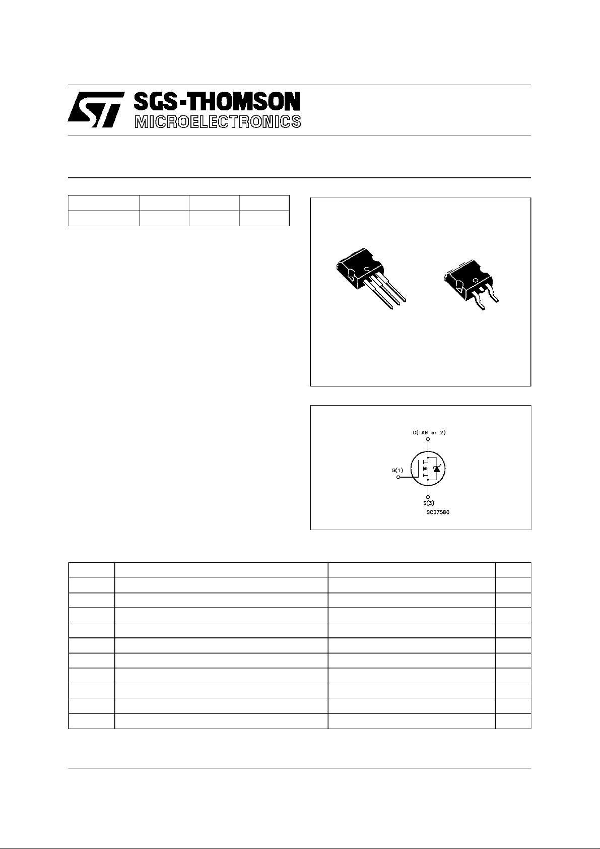
■ THROUGH-HOLE I2PAK (TO-262) POWER
PACKAGEIN TUBE(SUFFIX ”-1”)
■ SURFACE-MOUNTINGD2PACK (TO-263)
POWERPACKAGE IN TUBE (NO SUFFIX)
OR IN TAPE & REEL (SUFFIX ”T4”)
APPLICATIONS
■ HIGH CURRENT, HIGH SPEEDSWITCHING
■ SOLENOIDANDRELAY DRIVERS
■ REGULATORS
■ DC-DC& DC-AC CONVERTERS
■ MOTORCONTROL,AUDIO AMPLIFIERS
■ AUTOMOTIVEENVIRONMENT (INJECTION,
ABS, AIR-BAG,LAMPDRIVERS,Etc.)
3
2
1
I2PAK
TO-262
1
D2PAK
TO-263
INTERNAL SCHEMATIC DIAGRAM
3
ABSOLUTE MAXIMUM RATINGS
Symb o l Parame t er Val u e Uni t
V
V
DGR
V
I
DM
P
T
(•) Pulse width limited by safe operating area
March 1996
Drain-source Voltage (VGS= 0) 800 V
DS
Drain- gate Voltage (RGS=20kΩ) 800 V
Gate-source Voltage ± 30 V
GS
I
Drain Current (c ont inuo us) a t Tc=25oC4.7A
D
I
Drain Current (c ont inuo us) a t Tc=100oC3A
D
(•) Drain Current (puls ed) 19 A
Total Dissipat i on at Tc=25oC 125 W
tot
Derat ing Factor 1 W/
Stora ge Temperature -65 to 150
stg
T
Max. Operat ing Junct i on Temperatu re 150
j
o
o
o
C
C
C
1/10
Page 2
STB5NA80
THERMAL DATA
R
thj-case
R
thj-amb
R
thj-amb
T
AVALANCHE CHARACTERISTICS
Symb o l Para met er Max V alue Uni t
I
AR
E
E
I
AR
Ther mal Resistance Junct ion-case Max
Ther mal Resistance Junct ion-ambient Max
Ther mal Resistance Case-s i nk Typ
Maximum Lead Tempera t ure For Solder ing Purpo se
l
Avalanche Current , Repet it iv e or Not-Repe t it ive
(pulse width limi t ed by T
Single Pu lse Avalanc he E nerg y
AS
(starti ng T
Repetitive Avalanche Energy
AR
=25oC, ID=IAR,VDD=25V)
j
(pulse width limi t ed by T
max, δ <1%)
j
max, δ <1%)
j
Avalanche Current , Repet it iv e or Not-Repe t it ive
=100oC, p ulse wid t h limited by Tjmax, δ <1%)
(T
c
1
62.5
0.5
300
4.7 A
110 mJ
4.5 mJ
3A
o
C/W
o
C/W
o
C/W
o
C
ELECTRICAL CHARACTERISTICS (T
=25oC unlessotherwise specified)
case
OFF
Symbol Parameter Test Condition s Min. Typ. Max. Unit
V
(BR)DSS
Drain-source
ID= 250 µAV
= 0 800 V
GS
Break dow n Voltage
I
I
DSS
GSS
Zero Gate Voltage
Drain Current (V
GS
Gat e- bod y Leaka ge
Current (V
DS
=0)
=0)
=MaxRating
V
DS
V
=MaxRatingx0.8 Tc= 125oC
DS
V
= ± 30 V ±100 nA
GS
250
1000µAµA
ON (∗)
Symbol Parameter Test Condition s Min. Typ. Max. Unit
V
GS(th )
R
DS(on)
I
D(on)
Gat e Thre shold Volt age VDS=VGSID=250µA2.533.75V
St at ic Drain-source On
Resistance
VGS=10V ID=2.5A
=10V ID=2.5A Tc= 100oC
V
GS
On State Drain Current VDS>I
D(on)xRDS(on)maxVGS
=10 V 4.7 A
1.8 2.4
4.8
DYNAMIC
Symbol Parameter Test Condition s Min. Typ. Max. Unit
g
(∗)Forward
fs
Tr ansc on ductance
C
C
C
Input Capac it an ce
iss
Out put Capac itance
oss
Reverse Transfer
rss
Capacit a nc e
VDS>I
D(on)xRDS(on)maxID
=2.5A 2.7 5.2 S
VDS=25V f=1MHz VGS= 0 1250
140
35
1700
190
50
Ω
Ω
pF
pF
pF
2/10
Page 3
STB5NA80
ELECTRICAL CHARACTERISTICS (continued)
SWITCHINGON
Symbol Parameter Test Condition s Min. Typ. Max. Unit
t
d(on)
t
r
Turn-on Time
Rise Time
VDD=400V ID=2.5A
=4.7 Ω VGS=10V
R
G
(see test cir cuit, figure 3)
(di/dt)
Tur n-on C urr ent Slope VDD=640V ID=5A
on
R
=47 Ω VGS=10V
G
(see test cir cuit, figure 5)
Q
Q
Q
Tot al Gat e Charge
g
Gate-Source Charge
gs
Gat e- Drain Charge
gd
VDD= 640 ID=5A VGS=10V 55
SWITCHINGOFF
Symbol Parameter Test Condition s Min. Typ. Max. Unit
t
r(Voff)
t
Off -voltage Rise Time
t
Fall T ime
f
Cross-over Time
c
VDD=640V ID=5A
=47Ω VGS=10V
R
G
SOURCE DRAIN DIODE
40
10055135
180 A/ µs
75 nC
8
24
75
25
110
100
35
150
ns
ns
nC
nC
ns
ns
ns
Symbol Parameter Test Condition s Min. Typ. Max. Unit
I
I
SDM
SD
Source-drain Current
(•)
Source-drain Current
4.7
19
(pulsed)
(∗)ForwardOnVoltage ISD=4.7A VGS=0 1.6 V
V
SD
t
Q
Reverse Recovery
rr
Time
Reverse Recovery
rr
ISD= 5 A di/dt = 100 A/µs
=100V Tj=150oC
V
DD
800
15.2
Charge
I
RRM
Reverse Recovery
38
Current
(∗) Pulsed: Pulse duration =300 µs,duty cycle 1.5 %
(•) Pulse width limited by safe operating area
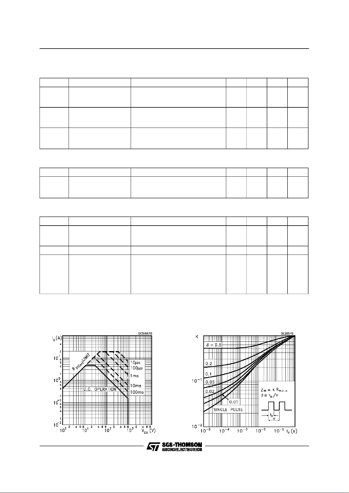
Safe Operating Area ThermalImpedance
A
A
ns
µC
A
3/10
Page 4

STB5NA80
Derating Curve
TransferCharacteristics
OutputCharacteristics
Transconductance
StaticDrain-source On Resistance
4/10
Gate Charge vs Gate-source Voltage
Page 5

STB5NA80
CapacitanceVariations
Normalized OnResistance vs Temperature
Normalized GateThreshold Voltage vs
Temperature
Turn-onCurrent Slope
Turn-offDrain-source VoltageSlope
Cross-overTime
5/10
Page 6

STB5NA80
SwitchingSafe Operating Area
Source-drainDiode Forward Characteristics
AccidentalOverload Area
Fig. 1: UnclampedInductive Load Test Circuit Fig.2: UnclampedInductive Waveform
6/10
Page 7

STB5NA80
Fig. 3: SwitchingTimes Test Circuits For
ResistiveLoad
Fig. 5: Test CircuitFor Inductive Load Switching
And DIodeRecovery Times
Fig. 4: GateCharge test Circuit
7/10
Page 8

STB5NA80
TO-262(I2PAK) MECHANICALDATA
DIM.
MIN. TYP. MAX. MIN. TYP. MAX.
A 4.3 4.6 0.169 0.181
A1 2.49 2.69 0.098 0.106
B 0.7 0.93 0.027 0.036
B1 1.2 1.38 0.047 0.054
B2 1.25 1.4 0.049 0.055
C 0.45 0.6 0.017 0.023
C2 1.21 1.36 0.047 0.053
D 9 9.35 0.354 0.368
e 2.44 2.64 0.096 0.104
E 10 10.28 0.393 0.404
L 13.2 13.5 0.519 0.531
L1 3.48 3.78 0.137 0.149
L2 1.27 1.37 0.050 0.054
mm inch
8/10
C
A
A1
C2
B2
B
e
E
L1
L2
D
L
Page 9

TO-263 (D2PAK) MECHANICAL DATA
STB5NA80
DIM.
MIN. TYP. MAX. MIN. TYP. MAX.
A 4.3 4.6 0.169 0.181
A1 2.49 2.69 0.098 0.106
B 0.7 0.93 0.027 0.036
B2 1.25 1.4 0.049 0.055
C 0.45 0.6 0.017 0.023
C2 1.21 1.36 0.047 0.053
D 9 9.35 0.354 0.368
E 10 10.28 0.393 0.404
G 4.88 5.28 0.192 0.208
L 15 15.85 0.590 0.624
L2 1.27 1.37 0.050 0.054
L3 1.4 1.75 0.055 0.068
mm inch
E
A
C2
L2
D
L
L3
B2
B
A1
C
G
9/10
Page 10

STB5NA80
Information furnished is believedto be accurateand reliable. However, SGS-THOMSON Microelectronics assumes no responsability for the
consequencesof use ofsuch informationnor for any infringement of patents or otherrights of third parties which may resultsfrom its use. No
licenseis grantedby implicationor otherwise underany patentor patentrights ofSGS-THOMSONMicroelectronics. Specificationsmentioned
in this publicationare subject to change without notice.This publication supersedes andreplacesall information previously supplied.
SGS-THOMSONMicroelectronics productsarenotauthorizedfor useascriticalcomponents inlife supportdevices or systems withoutexpress
writtenapproval of SGS-THOMSONMicroelectonics.
1995 SGS-THOMSONMicroelectronics - All Rights Reserved
Australia - Brazil- France - Germany - HongKong - Italy- Japan- Korea - Malaysia - Malta - Morocco- The Netherlands -
Singapore- Spain- Sweden - Switzerland- Taiwan - Thailand - United Kingdom- U.S.A
SGS-THOMSONMicroelectronicsGROUPOF COMPANIES
...
10/10
 Loading...