

Page 1
• ONE CHIP SYSTEM TO INTERFACE GPS
ANTENNA TO GPS MICRO CONTROLLER
• ABLE TO SUPPORT ACTI VE AND PASSIVE
ANTENNA
• MINIMUM EXTERNAL COMPONENTS
• COMPATIB LE WITH GPS L1 SPS SIGNAL AN D
GALILEO FREQU ENCIES
• CMOS OUTPUT LEVELS
• 2.7 V .. 3.6 V SUPPLY VO LTAGE
• EMBEDDED LOW PHASE NOISE PLL
• ACTIVE ANTENNA SENSOR
• SMART CHIP ENABLE FUNCTION FOR POWER
CONSUMPTION OPTIMIZATION
• ESD PROTECTED
STB5610
GPS RF FRONT-END IC
PRELIMINARY DATA
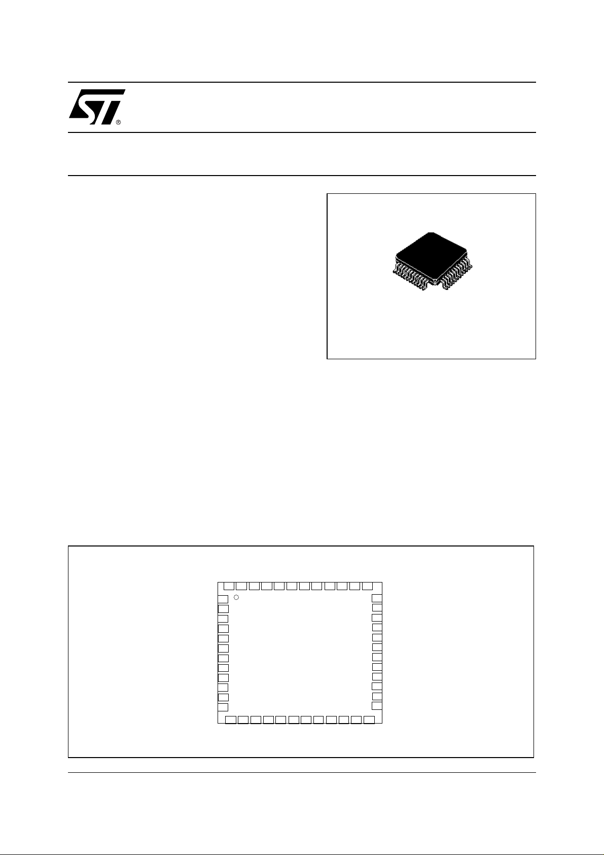
TQFP48
ORDER CODE
STB5610
BRANDING
STB5610
DESCRIPTION
The STB5610, using ST Microelectronics RF Bipolar
technology, implements a Global Positioning System
RF front-end. The chip provides down conversion
from the 1575.42 MHz GPS (L1) signal to 4.092 MHz
Output signal. The integrated PLL with on-chip
reference oscillator uses a low cost 16.368 MHz
crystal. No TCXO is required.
PIN CONNECTION
XTAL_out
R
F
+
L
A
n
i
T
F
_
X
I
L
_
_
A
d
c
c
n
T
V
X
G
LNA_out+
Gnd_RF
RF-
V
c
c
_
R
F
Vcc_XTAL
Vcc_Logic
Vcc_VCO
Gnd
TNK1
TNK2
Gnd
Gnd
IF1+
IF1Gnd
L
A
T
X
_
d
n
G
47 46 45 44 434241 40 39 38
47 46 45 44 434241 40 39 38 37
47 46 45 44 434241 40 39 38
47 46 45 44 434241 40 39 38
48
48
48
48
1
1
2
2
3
3
LF
4
4
5
5
6
6
7
7
8
8
9
9
10
10
11
11
12
13 14 15 16 17 18 19 20 21 22 23 24
Gnd_RF
F
I
_
-
d
2
n
F
I
G
IF2+
L
V
N
c
c
A
_
_
L
o
N
u
A
t
-
E
C
Gnd_IF
Fselect
CE2
36
Vcc_Logic2
35
Gnd
34
DATA
33
CLK
32
Gnd_Driver
31
Vcc_Driver
30
Gnd_Loic
29
Vcc_Logic
28
AS1
27
AS2
26
As_out
25
GC
G
LNA_in+
L
G
N
n
d
n
A
d
_
i
n
-
May, 7 2002
1/11
Page 2

STB5610
PIN CONFIGURATION
PIN Symbol Typ. DC Bias Description External Circuit
1 Vcc_XTAL Power supply
2 Vc c_Lo gic P ower suppl y
3 LF Loop filter
4 Vcc_VCO Power supply
5 Gnd Ground
6 TNK1 Tank Input
7 TNK2 Tank Input
8 Gnd Ground
9 Gnd Ground
10 IF1+ Mixer Output
11 IF1- Mixer Output
12 Gnd Ground
13 Gnd_RF Ground
14 RF+ RF amp. input
15 RF- RF amp. input
16 Gnd_RF Ground
17 Vcc_ RF Power supply
18 LNA_Out+ LNA output
19 LNA_Out- LNA output
20 Vcc_LNA Power supply
21 Gnd_L NA Ground
22 LNA_in+ LNA input
23 LNA_in- LNA input
24 Gnd_LNA Ground
2/11
Page 3

PIN CONFIGURATION
PIN Symbol Typ. DC Bias Description External Circuit
25 GC LNA Gain control
26 AS_Out Antenna sensor output
27 AS2 Antenna sensor input
28 AS1 Vcc Antenna Supply
29 Vc c_Lo gic P ower suppl y
30 Gnd_Logic Ground
31 Vcc_Driver Supply Voltage
32 Gnd_Driver Ground
33 CLK Clock
34 DATA Data
35 Gnd Ground
36 Vcc_Logic2 Supply Voltage
37 CE2 Chip Enable (no data)
38 CE Chip Enable
39 Fselect Frequency Selector
40 Gnd_IF Ground
41 IF2- Lim. Amp. Output
42 IF2+ Lim. Amp. Output
43 Gnd_IF Ground
44 Vcc_IF Supply Voltage
45 Gnd_XTAL Ground
46 XTAL_in Crystal Input
47 XTAL_out Crystal Output
48 Gnd_XTAL Ground
STB5610
3/11
Page 4

STB5610
BLOCK DIAGRAM (GPS L1)
SAW F ilt e r
Passive
Antenna
Two gain
LNA
Gain
Select.
16.368 MHz
Quartz
1.57 GHz
PLL
LC Filter
RF Amp. Mixer D Latc h Output buffer
1.55 GHz
VCO
~
LC Filter
1ST Lim. amp. 2ND Lim. amp.
20 MHz
20 MHz
D
Q
CK
4 MHz
16 MHz
Data @ 4 MHz
CMOS levels
CLK @ 16MHz
CMOS levels
Loop
Freq.
Filter
select
ExternalTank
FUNCTIONAL DESCRIPTION
LNA section
The RF input signal is amplified by two gain levels
LNA. Using gain control pin the LNA gain is set to
19 dB to support passive antenna or 10 dB to support active antenna. The LNA ou tput signal i s filtered by 1575.42 MHz SAW filter.
RF Amplifier plus mixer section
The 1575.42 MHz input signal, amplified by RF
amp., is mixed with the VCO signal to generate a
differential 20.46MHz IF signal
IF section
Two LC filters at mixer output and at first limiting
output are used to s uppress undesirab le signals
and mixer products. The second stage limiting
amplifier is connected to a D-Type latch clocked
by 16.368MHz crystal oscillator signal. The effect
of sampling the 20.46MHz signal at 16.368MHz is
to create sub-sampling alias at 4.092MHz. This is
fed to the output level converter.
Output section
The output buffers perform level translation from
the internal ECL levels to CMOS output levels referred to ground. The Data signal changes during
the clock signal negative edge.
CE
ASout
CE2
VCO and PLL
Using external tank the VCO is able to provide
very low phase noise signal. Through the freq. selector pin the VC O signal is set at 1554.96 M Hz
and at 1571.328 MHz. The on-chip ref erence oscillator uses a low cost 16.368 MHz crystal.
Antenna sensor circuitry
Integrated sensor circuitry is ab le to eval uate th e
antenna current consum ption; the As out pin output provides this info externally. Using external
sensing resistor of 10 Ohm if the antenna current
consumption is inside the range 10mA…40mA
(active antennas typical current consumption) the
Asout output logic level is High, if the antenna current consumption is outside the ab ove reported
range (passive anten na or problem on antenna
connection) the Asout output logic level is low.
Chip enable
Using the CE pin it is possible to switch off all the
chip ( neither data nor clock available).
Using CE2 pin it is possible to disable the analog
portion of the chip (no data available) maintaining
the digital portion active (Clock available) optimizing the chip current consumption.
Power supplies
The STB5610, has been designed to support
from 2.7 V to 3.6 V supply voltage.
4/11
Page 5

STB5610
ABSOLUTE MAXIMUM RATING
Symbol Parameter Value Unit
Vcc Supply voltage 5.9 V
Tj Junction operating temperature -40 to 125
THERMA L D ATA
Symbol Parameter Value Unit
2.1
o
C/W
Rthj-case Thermal resistance junction- case TBD
ELECTRICAL CHARACTERISTICS (Vcc = 3+/-10%, Tcase= 25 oC)
Symbol Parameter Test conditions Min. Typ. Max. Unit
SUPPLY
Vcc Supply voltage 2.7 3.3 3.6 V
Icc Supply current 37 mA
AS1
Vcc Antenna
Supply
2.7 3.3 / 5 5.5 V
LNA
Gp Power gain
NF Noise figure
IIP3 Input IP3
VSWRin
Voltage St at. Wave
Ratio
Pin GC at GND
Pin GC at Vcc
Pin GC at GND
Pin GC at Vcc
Pin GC at GND
Pin GC at Vcc
=50Ω
Z
L
19
10
3
10
-20
-5
o
C
dB
dB
dBm
RF AMPLIFIER AND MIXER CHAIN
IIP3 Input IP3 -19 dBm
NF Noise Figure 5.5 dB
Z
IN
Z
OUT
fRF Input signal RF 1.575 MHz
G
Input impedance 50 Ω
Differential output
impedance
Voltage Convertion
Gain
1.4 ΚΩ
30 dB
FIRST LIMI TI N G AM P L I FI ER
G Voltage Gain 60 dB
Z
OUT
Differential output
impedance
2.4 ΚΩ
5/11
Page 6

STB5610
ELECTRICAL CHARACTERISTICS (Vcc = 3+/-10%, Tcase= 25 oC)
Symbol Parameter Test conditions Min. Typ. Max. Unit
SECOND LIMITING AMPLIFIER
G Voltage Gain 30 dB
VCO
(GPS LO frequency 1555MHz)
VCO
Phase noise
∆f = 1KHz, SSB (10KHz PLL
closed loop bandwith)
-60 dBc/Hz
OUTPUT BUFFER
V
OH
V
OL
(square wave CMOS level)
High output voltage Vcc-0.4 Vcc V
Low output voltage 0 0+0.4 V
PHASE LOCKED LOOP
XTAL
INPUT CONTROL PINS TABLE
Reference crystal 16.368 MHz
(The logic levels are TTL compatible)
GC Pin (lna gain control pin)
Logic level Value
Low Max Gain
High Min Gain
CE2 Pin (Analog porti on e n a bl e pi n)
Logic level Value
Low Switch-o ff
High Switch-on
CE Pin (Tot al chip enable pin)
Logic level Value
Low Switch-off
High Switch-on
FSELECT ( Frequencie s Selector Pin)
Logic level Value
Low GPS frequency
High Galileo frequency
OUTPUT CONTROL PINS TABLE
The Asout pin output provides information on Antenna current consumption
ASout Pi n (A nt enna sensor pi n)
*
Logic level V alue
Low** Iant<10mA
Iant.>40mA
High** 10mA<Iant<40mA
* It is referred to external sensing resistor of 10 O Hm
Application requiring higher or lower current threshold should adjust the resistor value appropiately
** The logic levels are referred to STB5610 Supply Voltage
6/11
Page 7

APPLICATION BOARD SCHEMATIC (ACTIVE ANTENNA)
STB5610
T
S
QUE
A
V
A
I
L
A
B
L
E
ON
RE
7/11
Page 8

STB5610
APPLICATION BOARD LAYOUT (ACTIVE ANTENNA)
T
S
QUE
A
V
A
I
L
A
B
L
E
ON
RE
8/11
Page 9

BILL OF MATERIALS
STB5610
T
S
QUE
A
V
A
I
L
A
B
L
E
ON
RE
9/11
Page 10

STB5610
MECHANICAL DATA
mm
DIM.
A 1.60
A1 0.05 0.15
A2 1.35 1.40 1.45
D 8.75 9.00 9.25
D1 6.9 7.00 7.1
E 8.75 9.00 9.25
E1 6.9 7.00 7.1
L 0.5 0.60 0.75
e0.5
b 0.17 0.22 0.27
ccc 0.08
ddd 0.08
TETA
Note: L is measured at gage plane (at 0.25 above the seating plane)
MIN. TYP. MAX
o
0
o
7
10/11
Page 11

STB5610
Information furnished is believed to be accurate and reliable. However, STMicroelectronics assumes no responsibility for the consequences
of use of such information nor for any infringement of patents or other rights of third parties which may result from its use. No license is granted
by implic ation or otherwise under any patent or pat ent rights of STMicroelectronics. Specifications mentioned in thi s publicati on are subject
to change without notice. This publication supersedes and replaces all information previously supplied. STMicroelectronics products are not
authorized for use as cri tical comp onents in life support dev i ces or systems wi thout express written approval of STM i croelect ronics.
The ST logo is registered trademark of STMicroelectronics
2002 STMicroelectroni cs - All Righ ts Reserved
All other na m es are the prop erty of their respectiv e owners.
Austra lia - Brazil - Canada - Ch i na - F i nl and - Fran ce - Germany - Hong Kong - In di a - I srael - Italy - Japan -
Malaysi a - M alta - Moroc co - Singapore - Spain - Sw eden - Switz erland - Unit ed Kingdo m - U. S. A.
STMicroelectroni cs GROUP OF COMPANIES
http://www.st.co m
11/11
 Loading...