

Datasheet STP55NF06LFP, STP55NF06L, STB55NF06L-1, STB55NF06L Datasheet (SGS Thomson Microelectronics)
Page 1
STP55NF06L - STP55NF06LFP
STB55NF06L - STB55NF06L-1
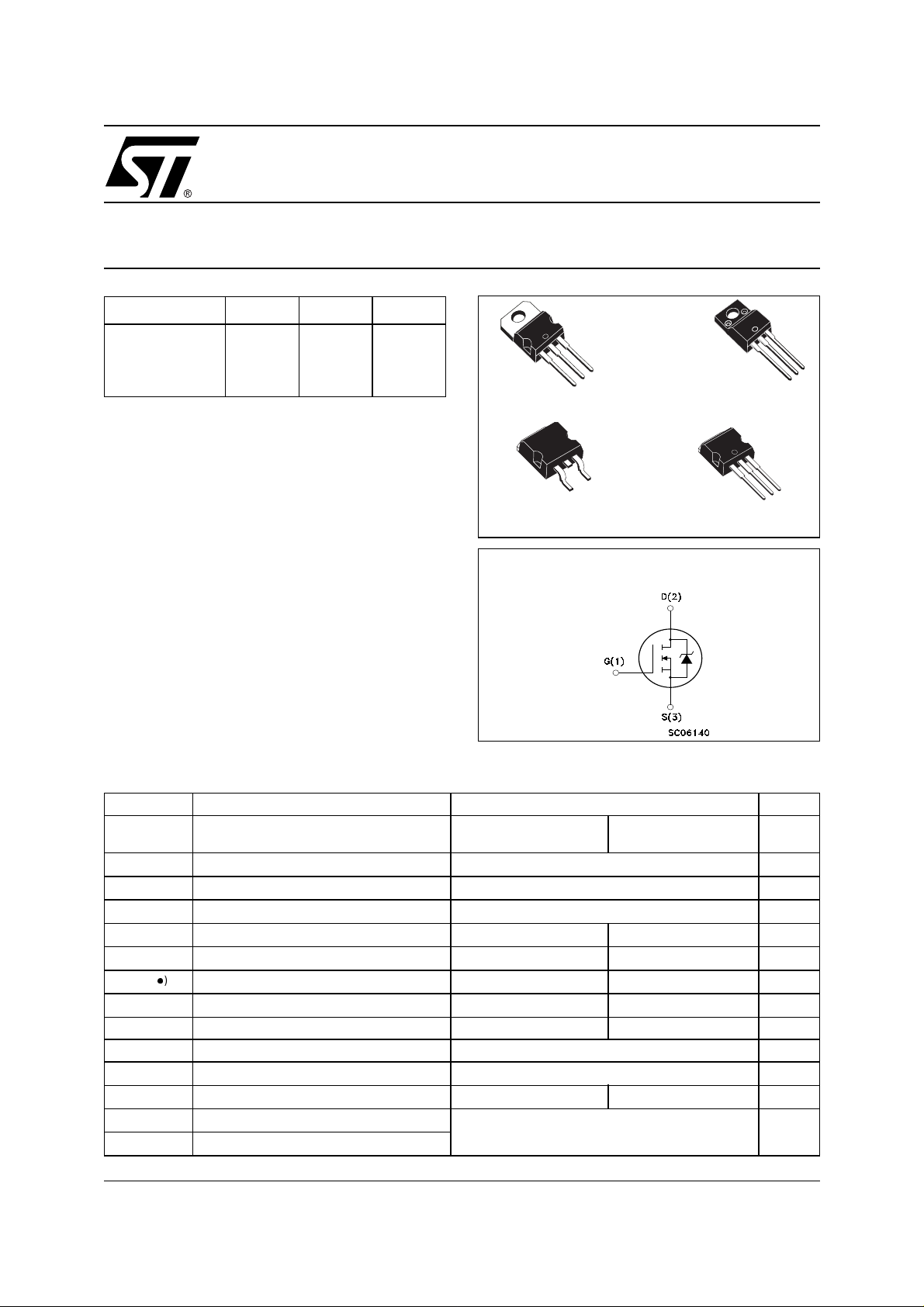
N-CHANNEL 60V - 0.014Ω - 55A TO-220/FP/D2PAK/I2PAK
STripFET™II POWER MOSFET
TYPE V
STP55NF06L
STP55NF06LFP
STB55NF06L
STB55NF06L-1
■ TYPICAL R
■ EXCEPTIONAL dv/dt CAPABILITY
■ APPLICATION ORIENTED
DS
DSS
60 V
60 V
60 V
60 V
(on) = 0.014Ω
R
DS(on)
<0.018 Ω
<0.018 Ω
<0.018 Ω
<0.018 Ω
I
D
55 A
55 A
55 A
55 A
CHARACTERIZATION
DESCRIPTION
This Power Mosfet is the latest development of
STMicroelectronics unique “Single Feature
™” strip-based process. The re sulting tran-
Size
sistor shows extremely high packing density for
low on-resistance, rugged avalance characteristics and less critical alignment steps therefore a remarkable manufacturing reproducibility.
APPLICATIONS
■ HIGH CURRENT, HIGH SPEED SWITCHING
■ MOTOR CONTROL, AUDIO AMPLIFIERS
■ DC-DC & DC-AC CONVERTERS
■ AUTOMOTIVE ENVI R ONM EN T (IN JECTION,
ABS, AIR-BAG, LAMPDRIVERS, Etc.)
3
2
1
TO-220
2
D
PAK
3
1
TO-220FP
I2PAK
INTERNAL SCHEMATIC DIAGRAM
3
2
1
3
2
1
ABSOLUTE MAXIMUM RATINGS
Symbol Parameter Value Unit
STP55NF06L
STB55NF06L/-1
Drain-source Voltage (VGS = 0)
Drain-gate Voltage (RGS = 20 kΩ)
Gate- source Voltage ± 16 V
Drain Current (continuous) at TC = 25°C
Drain Current (continuous) at TC = 100°C
(l)
Drain Current (pulsed) 220 120 A
Total Dissipation at TC = 25°C
55 30 A
39 21 A
95 30 W
V
I
DM
P
V
DGR
V
I
I
TOT
DS
GS
D
D
Derating Factor 0.63 0.2 W/°C
dv/dt (2) Peak Diode Recovery voltage slope 20 V/ns
(1)
E
AS
V
ISO
T
stg
T
j
(●) Pulse width limited by safe operating area
Single Pulse Avalanche Energy 300 mJ
Insulation Withstand Voltage (DC) - 2500 V
Storage Temperature
Max. Operating Junction Temperature
(1) Starting Tj=25°C, ID=27.5A, VDD=30V
≤ 55 A, di/dt ≤ 200A/µs, VDD ≤ V
(2) I
SD
– 55 to 175 °C
STP55NF06LFP
60 V
60 V
, Tj ≤ T
(BR)DSS
JMAX.
1/12August 2002
Page 2
STP55NF06L - STP55NF06LFP - STB 55NF06L - STB55NF06L-1
THERMA L D ATA
TO-220
2
PAK
D
2
I
PAK
Rthj-case Thermal Resistance Junction-case Max 1.58 5.0 °C/W
Rthj-amb Thermal Resistance Junction-ambient Max 62.5 °C/W
T
l
Maximum Lead Temperature For Soldering Purpose
ELECTRICAL CHARACTERISTICS (TCASE = 25 °C UNLESS OTHERWISE SPECIFIED)
OFF
Symbol Parameter Test Conditions Min. Typ. Max. Unit
V
(BR)DSS
I
DSS
I
GSS
(1)
ON
Symbol Parameter Test Conditions Min. Typ. Max. Unit
V
GS(th)
R
DS(on)
Drain-source
Breakdown Voltage
Zero Gate Voltage
Drain Current (V
GS
= 0)
Gate-body Leakage
Current (V
DS
= 0)
Gate Threshold Voltage
Static Drain-source On
Resistance
ID = 250 µA, VGS = 0 60 V
V
= Max Rating
DS
V
= Max Rating, TC = 125 °C
DS
V
= ± 16 V ±100 nA
GS
V
= VGS, ID = 250 µA
DS
1 1.7 V
VGS = 5 V, ID = 27.5 A
VGS = 10V, ID = 27.5 A
TO-220FP
300 °C
1µA
10 µA
0.016 0.020 Ω
0.014 0.018 Ω
DYNAMIC
Symbol Parameter Test Conditions Min. Typ. Max. Unit
(1)
g
fs
C
iss
C
oss
C
rss
Forward Transconductance
Input Capacitance
Output Capacitance 300 pF
Reverse Transfer
Capacitance
VDS = 15V , ID = 27.5 A
V
= 25V, f = 1 MHz, VGS = 0
DS
30 S
1700 pF
105 pF
2/12
Page 3
STP55NF06L - STP55NF06LF P - S TB55NF06L - STB55NF06L-1
ELECTRICAL CHARACTERISTICS (CONTINUED)
SWITCHING ON
Symbol Parameter Test Conditions Min. Typ. Max. Unit
V
t
d(on)
Q
Q
Q
t
r
g
gs
gs
Turn-on Delay Time
Rise Time 100 ns
Total Gate Charge
Gate-Source Charge
Gate-Drain Charge
SWITCHING OFF
Symbol Parameter Test Conditions Min. Typ. Max. Unit
t
d(off)
t
f
Turn-off-Delay Time
Fall Time
SOURCE DRAIN DIODE
Symbol Parameter Test Conditions Min. Typ. Max. Unit
I
SD
I
SDM
VSD (1)
t
rr
Q
rr
I
RRM
Note: 1. Pulsed: Pu l se duration = 300 µs, dut y c yc l e 1.5 %.
2. Pulse width li mited by safe operating area.
Source-drain Current 55 A
(2)
Source-drain Current (pulsed) 220 A
Forward On Voltage
Reverse Recovery Time
Reverse Recovery Charge
Reverse Recovery Current
= 30 V, ID = 27.5A
DD
RG= 4.7Ω VGS = 10V
(see test circuit, Figure 3)
= 48 V, ID = 55 A,
V
DD
VGS = 4.5V
VDD = 30 V, ID = 27.5 A,
RG=4.7Ω, V
GS
= 4.5V
(see test circuit, Figure 5)
ISD = 55 A, VGS = 0
= 55A, di/dt = 100A/µs,
I
SD
VDD = 30 V, Tj = 150°C
(see test circuit, Figure 5)
20 ns
27
37 nC
7
10
40
20
1.3 V
80
200
5
nC
nC
ns
ns
ns
nC
A
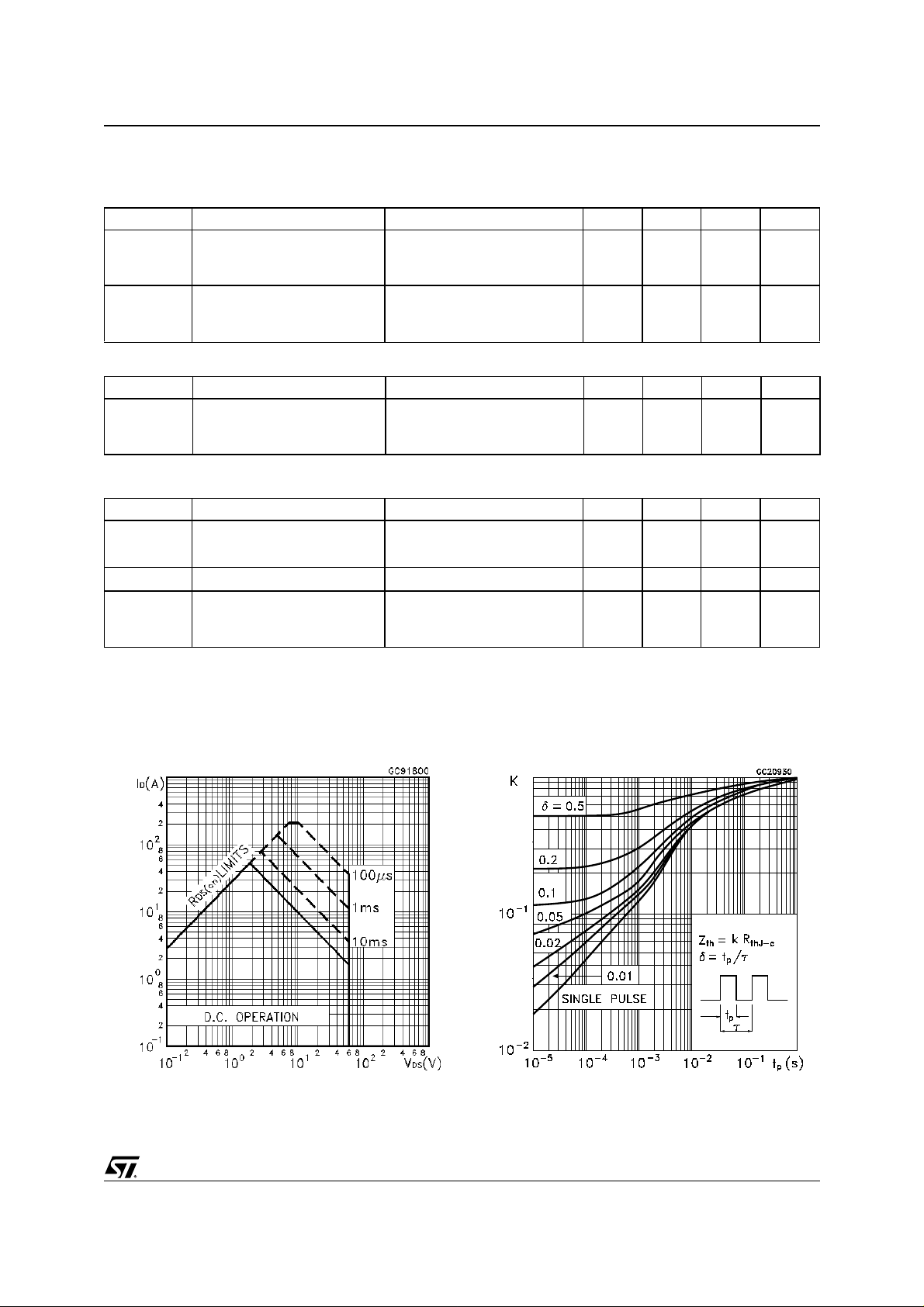
Thermal Impedance for TO-220/D2PAK/I2PAKSafe Operating Area For TO-220/D2PAK/I2PAK
3/12
Page 4
STP55NF06L - STP55NF06LFP - STB 55NF06L - STB55NF06L-1
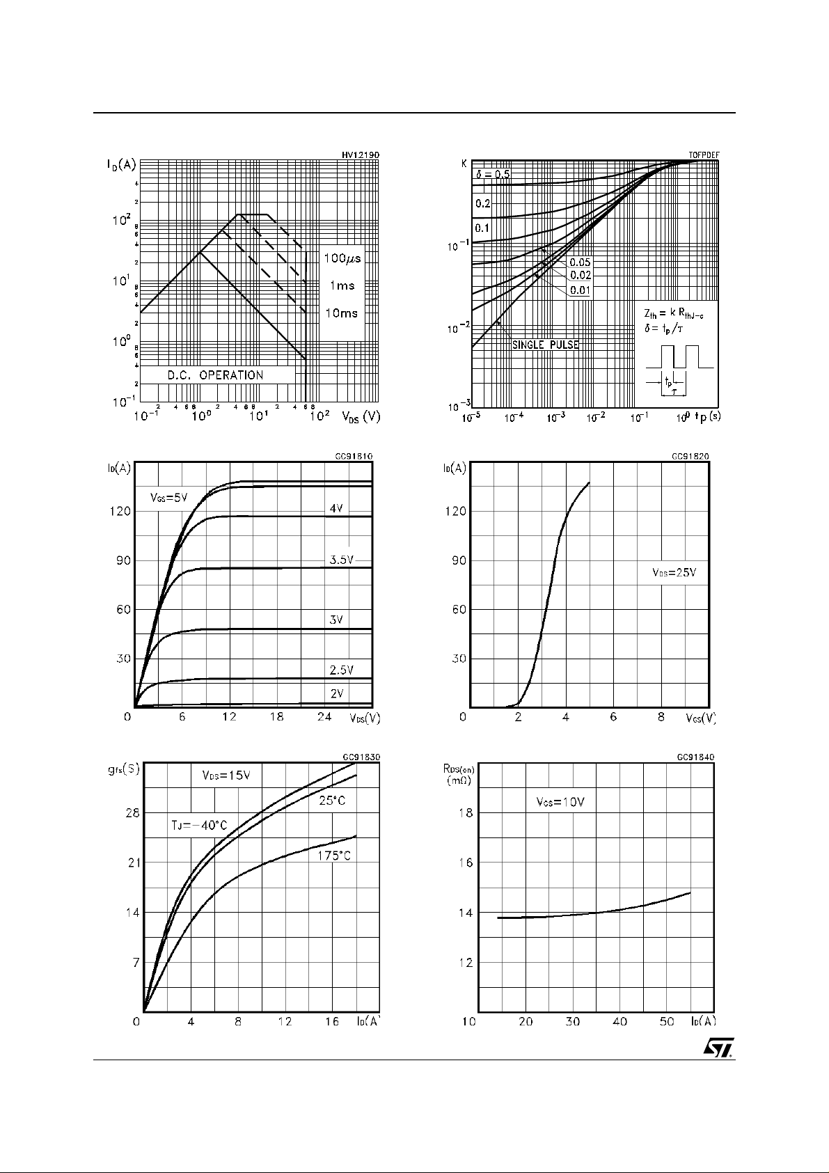
Safe Operating Area For TO-220FP
Output Characteristics
Thermal Impedance For TO-220FP
Transfer Characteristics
Transconductance
4/12
Static Drain-source On Resistance
Page 5
STP55NF06L - STP55NF06LF P - S TB55NF06L - STB55NF06L-1
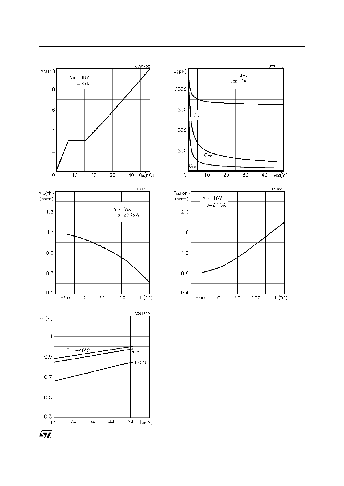
Capacitance VariationsGate Charge vs Gate-source Voltage
Normalized Gate Threshold Volta ge vs Temp.
Source-drain Diode Forward Characteristics
Normalized On Resistance vs Temperatur e
5/12
Page 6
STP55NF06L - STP55NF06LFP - STB 55NF06L - STB55NF06L-1
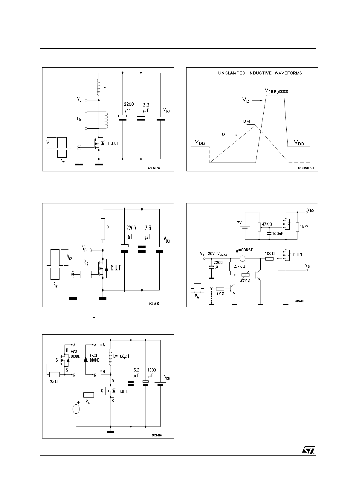
Fig. 2: Unclamped Inductive WaveformFig. 1: Unclamped Inductive Load Test Circuit
Fig. 3: Switching Times Test Circuit For
Resistive Load
Fig. 5: Test Circuit For Inductive Load Switching
And Diode Recovery Times
Fig. 4: Gate Charge test Circuit
6/12
Page 7
STP55NF06L - STP55NF06LF P - S TB55NF06L - STB55NF06L-1
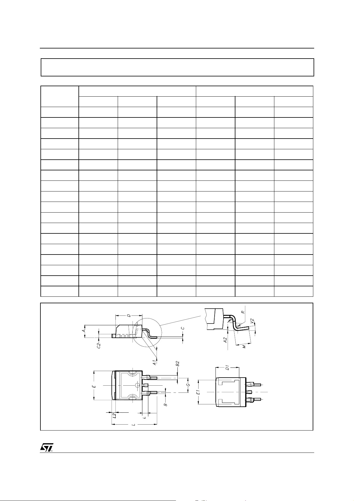
E
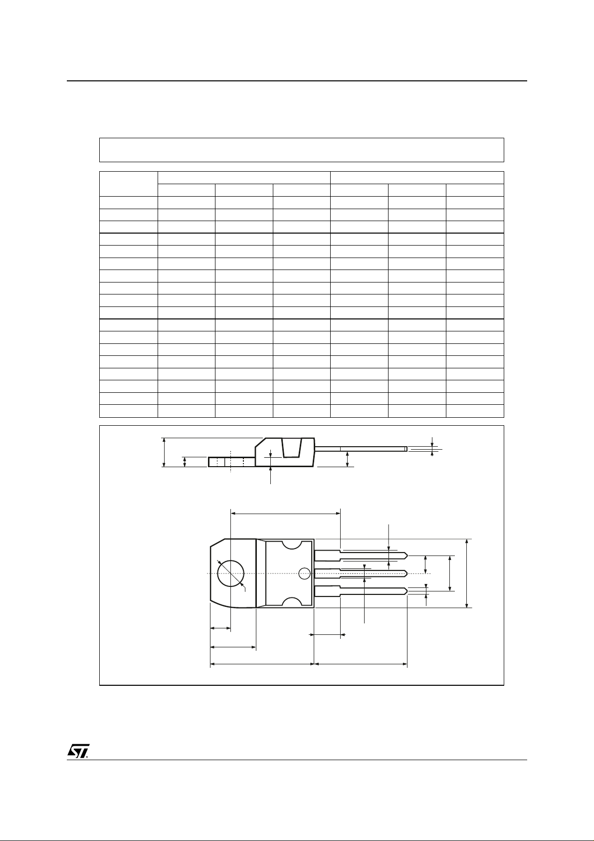
TO-220 MECHANICAL DATA
DIM.
A 4.40 4.60 0.173 0.181
C 1.23 1.32 0.048 0.051
D 2.40 2.72 0.094 0.107
D1 1.27 0.050
E 0.49 0.70 0.019 0.027
F 0.61 0.88 0.024 0.034
F1 1.14 1.70 0.044 0.067
F2 1.14 1.70 0.044 0.067
G 4.95 5.15 0.194 0.203
G1 2.4 2.7 0.094 0.106
H2 10.0 10.40 0.393 0.409
L2 16.4 0.645
L4 13.0 14.0 0.511 0.551
L5 2.65 2.95 0.104 0.116
L6 15.25 15.75 0.600 0.620
L7 6.2 6.6 0.244 0.260
L9 3.5 3.93 0.137 0.154
DIA. 3.75 3.85 0.147 0.151
MIN. TYP. MAX. MIN. TYP. MAX.
mm inch
A
C
D
L5
Dia.
L7
D1
L6
L2
L9
F1
G1
F
H2
G
F2
L4
P011C
7/12
Page 8
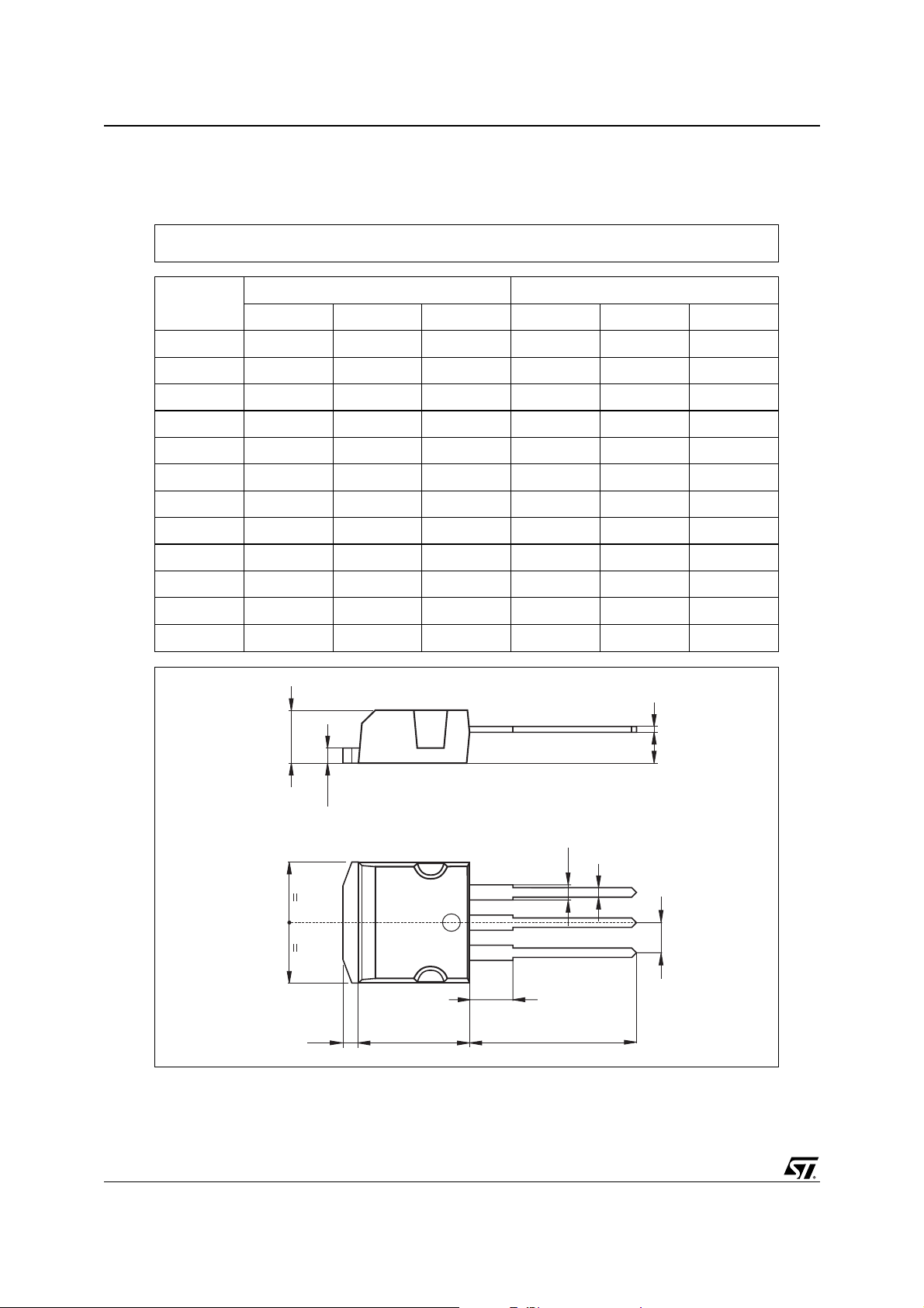
STP55NF06L - STP55NF06LFP - STB 55NF06L - STB55NF06L-1
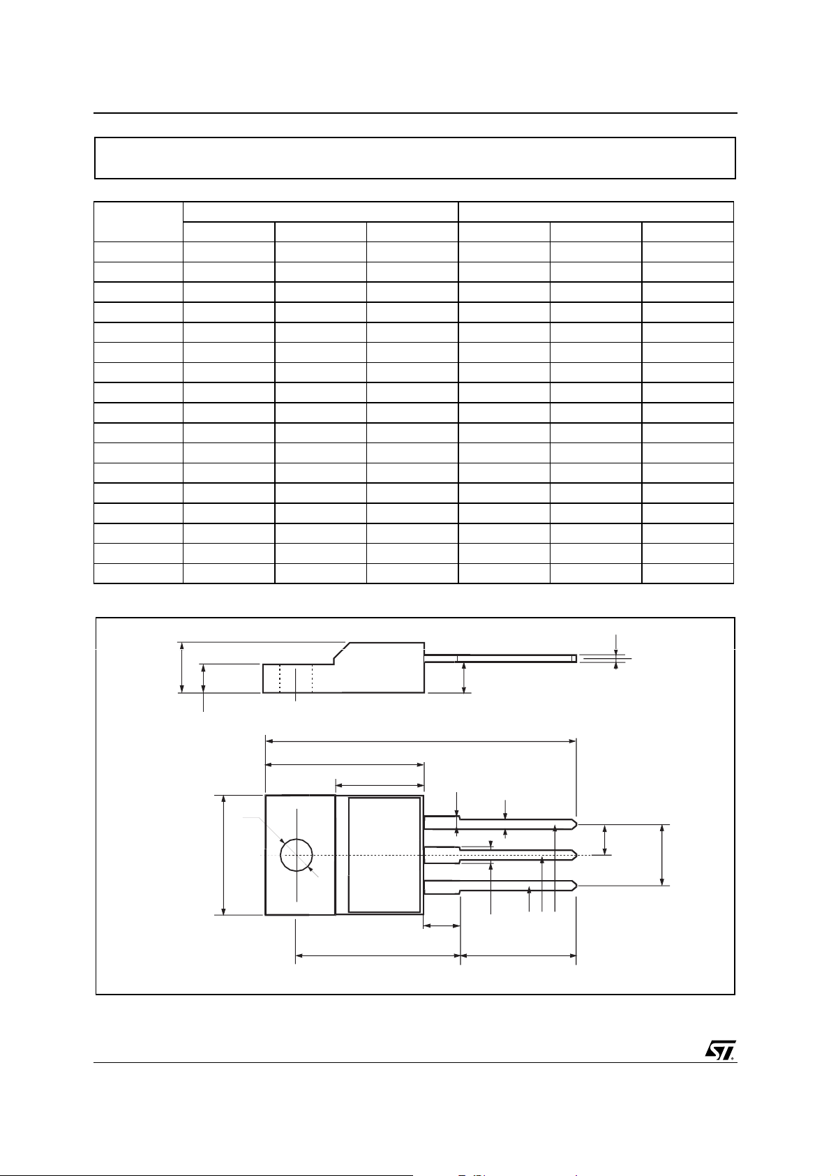
TO-220FP MECHANICAL DATA
DIM.
A 4.4 4.6 0.173 0.181
B 2.5 2.7 0.098 0.106
D 2.5 2.75 0.098 0.108
E 0.45 0.7 0.017 0.027
F 0.75 1 0.030 0.039
F1 1.15 1.7 0.045 0.067
F2 1.15 1.7 0.045 0.067
G 4.95 5.2 0.195 0.204
G1 2.4 2.7 0.094 0.106
H 10 10.4 0.393 0.409
L2 16 0.630
L3 28.6 30.6 1.126 1.204
L4 9.8 10.6 .0385 0.417
L5 2.9 3.6 0.114 0.141
L6 15.9 16.4 0.626 0.645
L7 9 9.3 0.354 0.366
Ø 3 3.2 0.118 0.126
MIN. TYP MAX. MIN. TYP. MAX.
mm. inch
E
A
D
B
L3
L6
L7
¯
F1
F
G1
H
G
F2
123
L2
L5
L4
8/12
Page 9
STP55NF06L - STP55NF06LF P - S TB55NF06L - STB55NF06L-1
2
D
PAK MECH ANICAL DATA
DIM.
MIN. TYP MAX. MIN. TYP. MAX.
A 4.4 4.6 0.173 0.181
A1 2.49 2.69 0.098 0.106
A2 0.03 0.23 0.001 0.009
B 0.7 0.93 0.027 0.036
B2 1.14 1.7 0.044 0.067
C 0.45 0.6 0.017 0.023
C2 1.23 1.36 0.048 0.053
D 8.95 9.35 0.352 0.368
D1 8 0.315
E 10 10.4 0.393
E1 8.5 0.334
G 4.88 5.28 0.192 0.208
L 15 15.85 0.590 0.625
L2 1.27 1.4 0.050 0.055
L3 1.4 1.75 0.055 0.068
mm. inch
M 2.4 3.2 0.094 0.126
R 0.4 0.015
V2 0º4º
3
9/12
1
Page 10
STP55NF06L - STP55NF06LFP - STB 55NF06L - STB55NF06L-1
TO-262 (I2PAK) MECHANICAL DATA
DIM.
MIN. TYP. MAX. MIN. TYP. MAX.
A 4.4 4.6 0.173 0.181
A1 2.49 2.69 0.098 0.106
B 0.7 0.93 0.027 0.036
B2 1.14 1.7 0.044 0.067
C 0.45 0.6 0.017 0.023
C2 1.23 1.36 0.048 0.053
D 8.95 9.35 0.352 0.368
e 2.4 2.7 0.094 0.106
E 10 10.4 0.393 0.409
L 13.1 13.6 0.515 0.531
L1 3.48 3.78 0.137 0.149
L2 1.27 1.4 0.050 0.055
mm inch
C
A
A1
10/12
C2
B2
B
e
E
L1
L2
D
L
P011P5/E
Page 11

STP55NF06L - STP55NF06LF P - S TB55NF06L - STB55NF06L-1
D2PAK FOOTPRINT
TAPE AND REEL SHIPMENT (suffix ”T4”)*
TUBE SHIPMENT (no suffix)*
REEL MECHANICAL DATA
TAPE MECHANICAL DATA
DIM.
A0 10.5 10.7 0.413 0.421
B0 15.7 15.9 0.618 0.626
D 1.5 1.6 0.059 0.063
D1 1.59 1.61 0.062 0.063
E 1.65 1.85 0.065 0.073
F 11.4 11.6 0.449 0.456
K0 4.8 5.0 0.189 0.197
P0 3.9 4.1 0.153 0.161
P1 11.9 12.1 0.468 0.476
P2 1.9 2.1 0.075 0.082
R 50 1.574
T 0.25 0.35 0.0098 0.0137
W 23.7 24.3 0.933 0.956
mm inch
MIN. MAX. MIN. MAX.
DIM.
A 330 12.992
B 1.5 0.059
C 12.8 13.2 0.504 0.520
D 20.2 0795
G 24.4 26.4 0.960 1.039
N 100 3.937
T 30.4 1.197
BASE QTY BULK QTY
mm inch
MIN. MAX. MIN. MAX.
1000 1000
* on s ales type
11/12
Page 12

STP55NF06L - STP55NF06LFP - STB 55NF06L - STB55NF06L-1
Information furnished is believed to be accurate and reliable. However, STMicroelectronics assumes no responsibility f or the
consequences of use of su ch in formation nor for any in fringement of patents or other rights of third parties w hich may result from
its use. No license is granted by implication or otherwise under any patent or patent rights of STMicroelectronics. Specifications
mentioned in this publication are subject to change without notice. This publication supersedes and replaces all information
previously suppli ed. STMi croelect ronics pr oducts are not author ized for use as cr itical component s in li fe suppo rt devi ces or
systems without express written approval of STMicroelectronics.
Australia - Brazil - Canada - China - Finland - France - Germany - Hong Kong - India - Israel - Italy - Japan - Malaysia - Malta - Morocco
© The ST logo is a registered trademark of STMicroelectronics
© 2002 STMicroelectronics - Printed in Italy - All Rights Reserved
Singapore - Spain - Sweden - Switzerland - United Kingdom - United States.
STMicroelectronics GROUP OF COMPANIES
© http://www.st.com
12/12
 Loading...