

Page 1
STB55NF06 STB55NF06-1
STP55NF06 STP55NF06FP
N-CHANNEL 60V - 0.015 Ω - 50A TO-220/ TO-220FP/I²PAK/D²PAK
STripFET™ II POWER MOSFET
TYPE
STP55NF06
STB55NF06-1
STB55NF06
STP55NF06FP
■ TYPICAL R
■ EXCEPTIONA L dv/d t CAPABILITY
■ 100% AVALANCHE TESTED
■ SURFACE-MOUNTING D
V
DSS
60 V
60 V
60 V
60 V
(on) = 0.015 Ω
DS
R
DS(on)
<0.018
Ω
<0.018
Ω
<0.018
Ω
<0.018
Ω
2
PAK (TO-263)
I
D
50 A
50 A
50 A
50 A(*)
POWER PACKAG E IN TU BE (NO SU FFIX) OR
IN TAPE & REEL (SUFFIX “T4”)
■ THROUGH-HOLE I²PAK (TO-262) POWER
PACKAGE IN TUBE (SUFFIX “- 1 ")
DESCRIPTION
This Power MOSFET is th e latest d evelopment of ST-
Microelectronis unique "Single Feature Size™" stripbased process. The resulting transistor shows extremely high packing density for low on-resistance,
rugged avalanche characteristics and less critical
alignment steps therefore a remarkable manufacturing reproducibility.
APPLICATIONS
■ HIGH CURRENT, HIGH SWITCHING SPEED
■ MOTOR CONTROL, AUDIO AMPLIFIERS
■ DC-DC & DC-AC CONVERTERS
■ AUTOMOTIVE
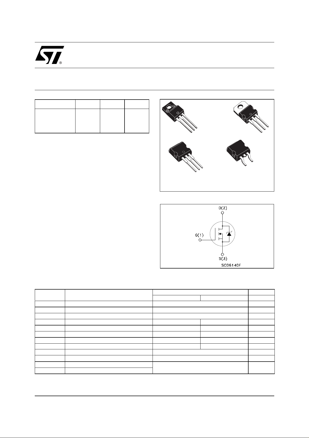
TO-220FP
1
²
PAK
I
TO-262
(Suffix “-1”)
3
2
3
2
1
TO-220
D²PAK
TO-263
(Suffix “T4”)
INTERNAL SCHEMATIC DIAGRAM
3
2
1
3
1
ABSOLUTE MAXIMUM RATINGS
Symbol Parameter Value Unit
STP_B55NF06(-1) STP55NF06FP
V
DS
V
DGR
V
GS
I
D
I
D
(
I
DM
P
tot
dv/dt
E
AS
T
stg
T
j
(
Pulse widt h l i m i ted by safe operating area
•)
(*)Refer to soa for the max allowable current value on FP-type due
to Rth value
.
Drain-source Voltage (VGS = 0)
Drain-gate Voltage (RGS = 20 kΩ)
60 V
60 V
Gate- source Voltage ± 20 V
Drain Current (continuous) at TC = 25°C
Drain Current (continuous) at TC = 100°C
•)
Drain Current (pulsed) 200 200(*) A
Total Dissipation at TC = 25°C
50 50(*) A
35 35(*) A
110 30 W
Derating Factor 0.73 0.2 W/°C
(1)
Peak Diode Recovery voltage slope 7 V/ns
(2)
Single Pulse Avalanche Energy 350 mJ
Storage Temperature
Operating Junction Temperature
(1)
ISD ≤50A, di/dt ≤400A/µs , VDD ≤ V
(2) Starting
-55 to 175 °C
Tj = 25 oC, ID = 25A, VDD= 30V
(BR)DSS
, Tj ≤ T
JMAX
1/12March 2003
Page 2
STB50NF06 STB55NF06-1 STP55NF06 ST P55NF06FP
THERMA L D ATA
I²PAK
D²PAK
TO-220
Rthj-case Thermal Resistance Junction-case Max 1.36 5 °C/W
Rthj-amb
T
l
Thermal Resistance Junction-ambient
Maximum Lead Temperature For Soldering Purpose
Max 62.5
(1.6 mm from case, for 10 sec)
TO-220FP
300
°C/W
°C
ELECTRICAL CHARACTERISTICS (T
= 25 °C unless otherwise specified)
case
OFF
Symbol Parameter Test Conditions Min. Typ. Max. Unit
I
= 250 µA, VGS = 0
D
V
= Max Rating
DS
V
= Max Rating TC = 125°C
DS
V
= ± 20 V
GS
60 V
1
10
±100 nA
ON
V
(BR)DSS
I
DSS
I
GSS
(*)
Drain-source
Breakdown Voltage
Zero Gate Voltage
Drain Current (V
GS
Gate-body Leakage
Current (V
DS
= 0)
= 0)
Symbol Parameter Test Conditions Min. Typ. Max. Unit
V
GS(th)
R
DS(on)
Gate Threshold Voltage
Static Drain-source On
= VGS I
DS
V
= 10 V ID = 27.5 A
GS
= 250 µA
D
234V
0.015 0.018
V
Resistance
DYNAMIC
Symbol Parameter Test Conditions Min. Typ. Max. Unit
(*)
g
fs
C
iss
C
oss
C
rss
Forward Transconductance
Input Capacitance
Output Capacitance
Reverse Transfer
Capacitance
V
= 15 V ID= 27.5 A
DS
= 25V, f = 1 MHz, VGS = 0
V
DS
18 S
1530
300
105
µA
µA
Ω
pF
pF
pF
2/12
Page 3
STB50NF06 STB55NF06-1 STP55NF 06 STP55NF06FP
ELECTRICAL CHARACTERISTICS (continued)
SWITCHING ON
Symbol Parameter Test Conditions Min. Typ. Max. Unit
= 30 V ID = 27.5 A
t
d(on)
Turn-on Delay Time
t
r
Rise Time
V
DD
R
= 4.7 Ω VGS = 10 V
G
(Resistive Load, Figure 3)
Q
g
Q
gs
Q
gd
Total Gate Charge
Gate-Source Charge
Gate-Drain Charge
= 48 V ID= 55 A VGS= 10V
V
DD
SWITCHING OFF
Symbol Parameter Test Conditions Min. Typ. Max. Unit
= 30V ID = 27.5 A
t
d(off)
Turn-off Delay Time
t
f
Fall Time
V
DD
R
= 4.7Ω, V
G
GS
= 10 V
(Resistive Load, Figure 3)
SOURCE DRAIN DIODE
Symbol Parameter Test Conditions Min. Typ. Max. Unit
I
SD
I
SDM
V
SD
t
rr
Q
rr
I
RRM
(*)
Pulsed: P ul se duration = 300 µs, duty cycle 1.5 %.
(
•)Pulse width limited by s af e operating area.
Source-drain Current
(•)
Source-drain Current (pulsed)
(*)
Forward On Voltage
Reverse Recovery Time
Reverse Recovery Charge
Reverse Recovery Current
I
= 55A VGS = 0
SD
= 55 A di/dt = 100A/µs
I
SD
V
= 30 V Tj = 150°C
DD
(see test circuit, Figure 5)
16
8
44.5
10.5
17.5
36
15
75
170
4.5
60 nC
50
200
1.5 V
ns
ns
nC
nC
ns
ns
A
A
ns
nC
A
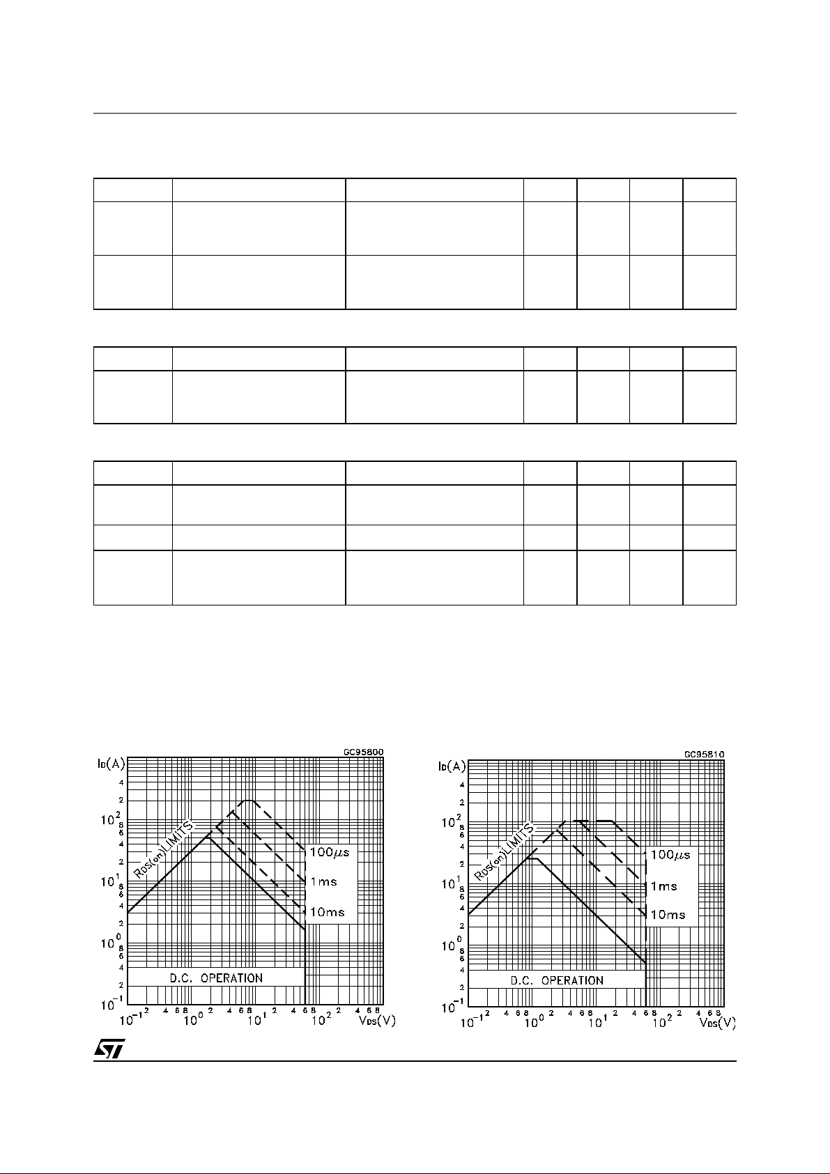
Safe Operating Area for TO-220FPSafe Operating Area for
3/12
Page 4
STB50NF06 STB55NF06-1 STP55NF06 ST P55NF06FP
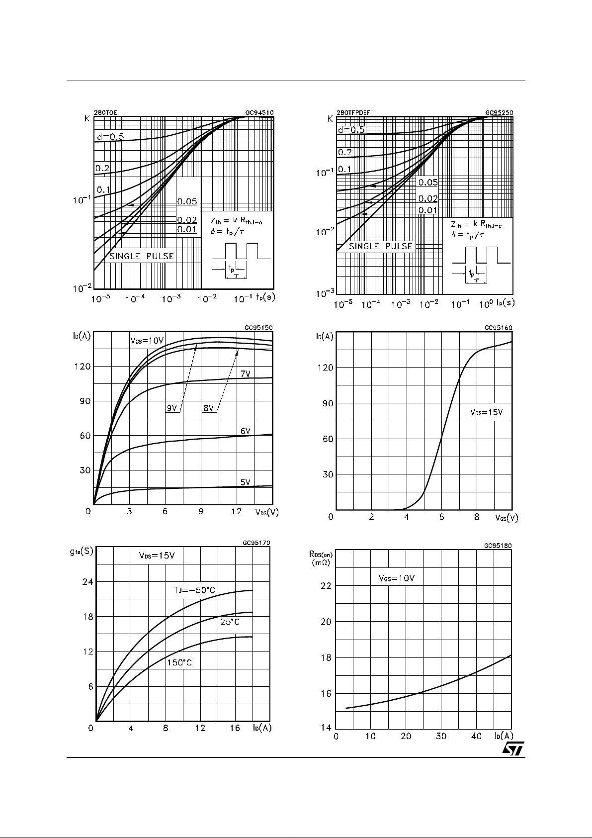
Thermal Impedance Thermal Impedance for TO-220FP
Output Characteristics Transfer Characteristics
Transconductance Static Drain-source On Resistance
4/12
Page 5

STB50NF06 STB55NF06-1 STP55NF 06 STP55NF06FP
Gate Charge vs Gate-source Voltage Capacitance Variations
Normalized Gate Threshold Voltage vs Temperature Normalized on Resistance vs Temperature
Source-drain Diode Forward Characteristics Normalized Breakdown Voltage Temperature
5/12
Page 6

STB50NF06 STB55NF06-1 STP55NF06 ST P55NF06FP
Fig. 1: Unclamped Inductive Load Test CircuitFig. 1: Unclamped Inductive Load Test Circuit Fig. 2: Unclamped Inductive Waveform
Fig. 3: Switching Times Test Circuits For Resistive
Load
Fig. 5: Test Circuit For Inductive Load Switching
And Diode Recovery Times
Fig. 4: Gate Charge test Circuit
6/12
Page 7

STB50NF06 STB55NF06-1 STP55NF 06 STP55NF06FP
D2PAK MECHANICAL DATA
DIM.
A 4.4 4.6 0.173 0.181
A1 2.49 2.69 0.098
A2 0.03 0.23 0.001 0.009
B 0.7 0.93 0.028 0.037
B2 1.14 1.7 0.045 0.067
C 0.45 0.6 0.018 0.024
C2 1.21 1.36 0.048 0.054
D 8.95 9.35 0.352 0.368
D1 8 0.315
E 10 10.4 0.394 0.409
E1 8.5 0.334
G 4.88 5.28 0.192 0.208
L 15 15.85 0.591 0.624
L2 1.27 1.4 0.050 0.055
L3 1.4 1.75 0.055 0.069
M 2.4 3.2 0.094 0.126
R 0.4 0.015
V2 0° 8° 0° 8°
MIN. TYP. MAX. MIN. TYP. TYP.
mm. inch.
0.106
7/12
Page 8

STB50NF06 STB55NF06-1 STP55NF06 ST P55NF06FP
E
TO-220 MECHANICAL DATA
DIM.
MIN. TYP. MAX. MIN. TYP. MAX.
A 4.40 4.60 0.173 0.181
C 1.23 1.32 0.048 0.051
D 2.40 2.72 0.094 0.107
D1 1.27 0.050
E 0.49 0.70 0.019 0.027
F 0.61 0.88 0.024 0.034
F1 1.14 1.70 0.044 0.067
F2 1.14 1.70 0.044 0.067
G 4.95 5.15 0.194 0.203
G1 2.4 2.7 0.094 0.106
H2 10.0 10.40 0.393 0.409
L2 16.4 0.645
L4 13.0 14.0 0.511 0.551
L5 2.65 2.95 0.104 0.116
L6 15.25 15.75 0.600 0.620
L7 6.2 6.6 0.244 0.260
L9 3.5 3.93 0.137 0.154
DIA. 3.75 3.85 0.147 0.151
mm inch
A
C
D
D1
L2
F1
L5
Dia.
G1
F
F2
L9
G
H2
L7
L6
L4
P011C
8/12
Page 9

STB50NF06 STB55NF06-1 STP55NF 06 STP55NF06FP
TO-262 (I2PAK) MECHANICAL DATA
DIM.
MIN. TYP. MAX. MIN. TYP. MAX.
A 4.4 4.6 0.173 0.181
A1 2.49 2.69 0.098 0.106
B 0.7 0.93 0.027 0.036
B2 1.14 1.7 0.044 0.067
C 0.45 0.6 0.017 0.023
C2 1.23 1.36 0.048 0.053
D 8.95 9.35 0.352 0.368
e 2.4 2.7 0.094 0.106
E 10 10.4 0.393 0.409
L 13.1 13.6 0.515 0.531
L1 3.48 3.78 0.137 0.149
L2 1.27 1.4 0.050 0.055
mm inch
C
A
A1
C2
B2
B
e
E
L1
L2
D
L
P011P5/E
9/12
Page 10

STB50NF06 STB55NF06-1 STP55NF06 ST P55NF06FP
TO-220FP MECHANICAL DAT A
DIM.
MIN. TYP. MAX. MIN. TYP. MAX.
A 4.4 4.6 0.173 0.181
B 2.5 2.7 0.098 0.106
D 2.5 2.75 0.098 0.108
E 0.45 0.7 0.017 0.027
F 0.75 1 0.030 0.039
F1 1.15 1.7 0.045 0.067
F2 1.15 1.7 0.045 0.067
G 4.95 5.2 0.195 0.204
G1 2.4 2.7 0.094 0.106
H 10 10.4 0.393 0.409
L2 16 0.630
L3 28.6 30.6 1.126 1.204
L4 9.8 10.6 0.385 0.417
L6 15.9 16.4 0.626 0.645
L7 9 9.3 0.354 0.366
Ø 3 3.2 0.118 0.126
mm inch
A
B
H
E
D
L3
L6
L7
¯
F1
F
G1
G
F2
123
L2
L4
10/12
Page 11

STB50NF06 STB55NF06-1 STP55NF 06 STP55NF06FP
D2PAK FOOTPRINT
TA PE AND REEL SHIPMENT (suffix ”T4”)*
TUBE SHIPMENT (no suffix)*
REEL MECHANICAL DATA
DIM.
A 330 12.992
B 1.5 0.059
C 12.8 13.2 0.504 0.520
D 20.2 0.795
G 24.4 26.4 0.960 1.039
N 100 3.937
T 30.4 1.197
mm inch
MIN. MAX. MIN. MAX.
TAPE MECHANICAL DATA
DIM.
A0 10.5 10.7 0.413 0.421
B0 15.7 15.9 0.618 0.626
D 1.5 1.6 0.059 0.063
D1 1.59 1.61 0.062 0.063
E 1.65 1.85 0.065 0.073
F 11.4 11.6 0.449 0.456
K0 4.8 5.0 0.189 0.197
P0 3.9 4.1 0.153 0.161
P1 11.9 12.1 0.468 0.476
P2 1.9 2.1 0075 0.082
R50 1.574
T0.25 0.35 .0.0098 0.0137
W 23.7 24.3 0.933 0.956
mm inch
MIN. MAX. MIN. MAX.
* on sales type
BASE QTY BULK QTY
1000 1000
11/12
Page 12

STB50NF06 STB55NF06-1 STP55NF06 ST P55NF06FP
Information furnished is believed to be accurate and reliable. However, STMicroelectronics assumes no responsibility for the consequences
of use of such information nor for any infringement of patents or other rights of third parties which may result from its use. No license is granted
by implic ation or otherwise under any patent or p at ent rights of STMicroelectronics. Spec i fications mentioned in this publicatio n are subject
to change without notice. This publication supersedes and replaces all information previously supplied. STMicroelectronics products are not
authorized for use as cri t i cal compone nts in life support device s or systems without express written approval of STM i croelectr onics.
The ST logo is registered trademark of STMicroelectronics
2003 STMi croelectr oni cs - All Righ ts Reserved
All other na m es are the prop erty of their respective owners.
Australi a - Brazil - Canada - Chin a - F i nl and - France - Germany - H ong Kong - Ind ia - Is rael - Italy - Japan - Malay sia - Malt a - Morocco -
Singap ore - Spain - Sweden - Swit zerland - Uni ted Kingdom - United States.
STMicroelectronics GROUP OF COMPANIES
http:// www.st.com
12/12
 Loading...