

Page 1
STB55NF03L
N-CHANNEL 30V - 0.01
TYPE V
ST B55NF03L 30 V < 0. 013 Ω 55 A
■ TYPICALR
■ OPTIMIMIZEDFOR HIGH SWITCHING
DS(on)
DSS
= 0.01 Ω
OPERATIONS
■ LOW GATE CHARGE
■ LOGICLEVEL GATE DRIVE
DESCRIPTION
This Power Mosfet is the latest development of
STMicroelectronics unique ”Single Feature
Size” strip-basedprocess. The resulting transistor shows extremely high packing density forlow
on-resistance, rugged avalance characteristics
and less critical alignment steps therefore a remarkablemanufacturingreproducibility.
APPLICATIONS
■ LOW VOLTAGEDC-DC CONVERTERS
■ HIGHCURRENT, HIGHSPEED SWITCHING
■ HIGHEFFICIENCY SWITCHINGCIRCUITS
R
DS(on)
I
D
Ω
- 55A D2PAK
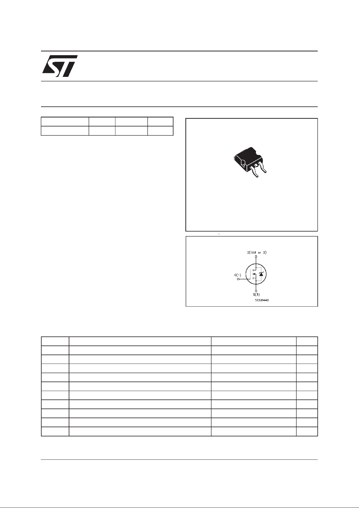
STripFET POWER MOSFET
3
1
D2PAK
TO-263
ADD SUFFIX ”T4”FOR ORDERING INTAPE & REEL
INTERNAL SCHEMATIC DIAGRAM
ABSOLUTE MAXIMUM RATINGS
Symbol Parameter Value Unit
V
V
V
I
DM
P
T
(•) Pulsewidth limited by safeoperating area
10/01/2000
Dra in- sour c e Volt age (VGS=0) 30 V
DS
Dra in- gate Volt age (RGS=20kΩ)30V
DGR
Gat e-source Voltage
GS
I
Dra in Current (c ont in uous ) at Tc=25oC55A
D
I
Dra in Current (c ont in uous ) at Tc=100oC39A
D
(•) D rain Cu rr ent (p ulsed) 220 A
Tot al Dissipation at Tc=25oC80W
tot
Der ati ng Fac t or 0.53 W/
St orage Tem pe rat ure -65 to 175
stg
T
Max. Operating Junct ion Temper at ur e 175
j
20 V
±
o
C
o
C
o
C
1/8
Page 2
STB55NF03L
THERMAL DATA
R
thj-case
R
thj-amb
T
Ther mal Resistanc e Junct ion-case Max
Ther mal Resistanc e Junct ion-ambient Max
Maximum Lead T emperat ur e For Soldering Purpose
l
1.875
62.5
300
o
C/W
o
C/W
o
C
ELECTRICAL CHARACTERISTICS
=25oC unless otherwisespecified)
(T
case
OFF
Symbol Parameter Test Conditions Min. Typ. Max. U nit
V
(BR)DSS
Drain-source
ID=250µAVGS=0 30 V
Break dow n Voltage
I
DSS
I
GSS
Zero Gate Voltage
Drain Current (V
GS
Gat e- bod y Leakage
Current (V
DS
=0)
=0)
V
=MaxRating
DS
=MaxRating Tc=125oC
V
DS
V
= ± 20 V ± 100 nA
GS
1
10
ON(∗)
Symbol Parameter Test Conditions Min. Typ. Max. U nit
V
GS(th)
R
DS(on)
I
D(on)
Gate Threshold Voltage VDS=VGSID= 250 µA12.5V
Sta t ic Dr ain -s ource O n
Resistance
On State Drain Current VDS>I
VGS=10V ID=27.5A
V
=4.5V ID=27.5A
GS
D(on)xRDS(on)max
0.01
0.015
0.013
0.021
55 A
VGS=10V
DYNAMIC
Symbol Parameter Test Con ditions Min. Typ. Max. Unit
g
(∗)Forward
fs
Tr ansc on duc tance
C
C
C
Input C apac i t ance
iss
Out put Capacitanc e
oss
Reverse T r ansfer
rss
Capacit a nc e
VDS>I
D(on)xRDS(on)maxID
=27. 5 A 40 S
VDS=25V f=1MHz VGS= 0 1450
390
150
µA
µ
Ω
Ω
pF
pF
pF
A
2/8
Page 3
STB55NF03L
ELECTRICAL CHARACTERISTICS
(continued)
SWITCHINGON
Symbol Parameter Test Con ditions Min. Typ. Max. Unit
t
d(on)
t
Tur n-on Delay Time
Rise T i me
r
VDD=15V ID= 27.5 A
R
=4.7
G
Ω
VGS=4.5V
25
280
(Resis t iv e Load, see f ig. 3)
Q
Q
Q
Tot al G at e Char ge
g
Gat e- Source Char g e
gs
Gate-Drain Charge
gd
VDD=24V ID=55A VGS=4.5V 25
11
12
35 nC
SWITCHINGOFF
Symbol Parameter Test Con ditions Min. Typ. Max. Unit
t
d(off)
Tur n-of f Delay Time
t
Fall T ime
f
VDD=15V ID= 27.5 A
=4.7 Ω VGS=4.5V
R
G
40
60
(Resis t iv e Load, see f ig. 3)
SOURCEDRAINDIODE
Symbol Parameter Test Con ditions Min. Typ. Max. Unit
I
SD
I
SDM
V
SD
t
Q
I
RRM
(∗) Pulsed: Pulse duration = 300µs, duty cycle 1.5 %
(•) Pulse width limited by safe operating area
Source-drain Current
(•)
Source-drain Current
55
220
(pulsed)
(∗)ForwardOnVoltage ISD=55A VGS=0 1.3 V
Reverse Re covery
rr
Time
Reverse Re covery
rr
ISD= 55 A di/dt = 100 A/µs
=15V Tj=150oC
V
DD
(see test circuit, fig. 5)
45
52
Charge
Reverse Re covery
2.3
Current
ns
ns
nC
nC
ns
ns
A
A
ns
nC
A
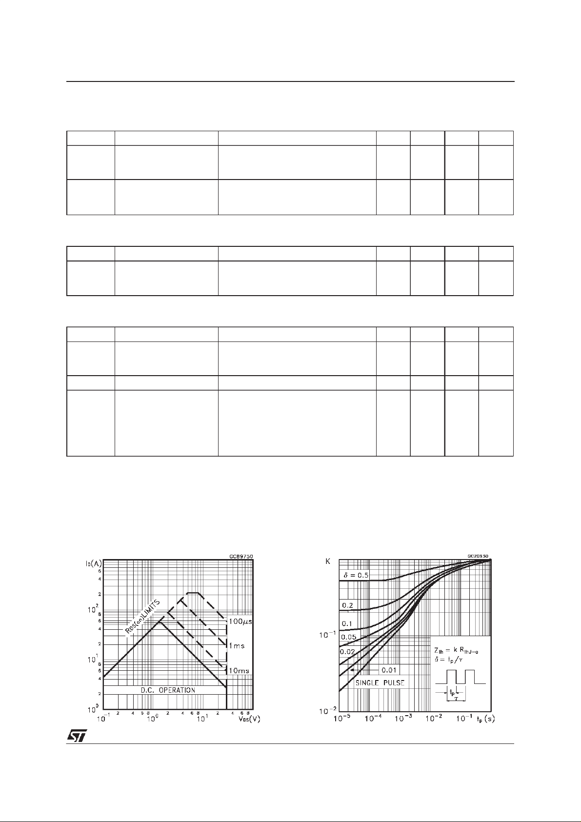
SafeOperating Area ThermalImpedance
3/8
Page 4

STB55NF03L
OutputCharacteristics
Transconductance
TransferCharacteristics
Static Drain-sourceOn Resistance
Gate Charge vs Gate-sourceVoltage
4/8
CapacitanceVariations
Page 5

STB55NF03L
NormalizedGate ThresholdVoltage vs
Temperature
Source-drainDiode Forward Characteristics
NormalizedOn Resistancevs Temperature
5/8
Page 6

STB55NF03L
Fig. 1
: UnclampedInductive LoadTest Circuit
Fig. 3: Switching Times Test Circuits For
ResistiveLoad
Fig. 2
: UnclampedInductiveWaveform
Fig. 4: Gate Charge test Circuit
Fig. 5
: Test Circuit For InductiveLoad Switching
And Diode Recovery Times
6/8
Page 7

TO-263 (D2PAK) MECHANICAL DATA
STB55NF03L
DIM.
MIN. TYP. MAX. MIN. TYP. MAX.
A 4.4 4.6 0.173 0.181
A1 2.49 2.69 0.098 0.106
B 0.7 0.93 0.027 0.036
B2 1.14 1.7 0.044 0.067
C 0.45 0.6 0.017 0.023
C2 1.21 1.36 0.047 0.053
D 8.95 9.35 0.352 0.368
E 10 10.4 0.393 0.409
G 4.88 5.28 0.192 0.208
L 15 15.85 0.590 0.624
L2 1.27 1.4 0.050 0.055
L3 1.4 1.75 0.055 0.068
mm inch
D
A
C2
DETAIL”A”
C
A2
DETAIL”A”
A1
B2
E
L2
L
L3
B
G
P011P6/E
7/8
Page 8

STB55NF03L
Information furnishedis believedto beaccurate and reliable.However, STMicroelectronics assumes no responsibilityfor the consequences
of use of such information nor for any infringement of patents or other rights of third parties which may result from its use. No license is
granted by implication or otherwise under any patent or patent rights of STMicroelectronics. Specificationmentioned in this publicationare
subjectto change without notice. This publication supersedes andreplaces all information previouslysupplied. STMicroelectronicsproducts
are not authorized for useas criticalcomponents in lifesupport devicesor systemswithout express written approval of STMicroelectronics.
The ST logo is a trademark of STMicroelectronics
1999 STMicroelectronics – Printed in Italy – All Rights Reserved
STMicroelectronics GROUP OF COMPANIES
Australia - Brazil - China - Finland - France - Germany - Hong Kong - India - Italy - Japan - Malaysia - Malta - Morocco -
8/8
Singapore - Spain - Sweden - Switzerland - United Kingdom - U.S.A.
http://www.st.com
.
 Loading...