

Page 1

STB55NE06
N - CHANNEL ENHANCEMENT MODE
” SINGLEFEATURE SIZE ” POWER MOSFET
TYPE V
DSS
R
DS(on)
I
D
STB55NE06 60 V < 0.022 Ω 55 A
■ TYPICALR
■ EXCEPTIONALdv/dt CAPABILITY
■ 100% AVALANCHETESTED
■ LOW GATE CHARGE 100
■ HIGH dv/dt CAPABILITY
■ APPLICATIONORIENTED
DS(on)
=0.019 Ω
o
C
CHARACTERIZATION
■ FOR THROUGH-HOLE VERSION CONTACT
SALESOFFICE
DESCRIPTION
This Power Mosfet is the latest development of
SGS-THOMSON unique ”Single Feature Size”
strip-based process. The resulting transistor
shows extremely high packing density for low onresistance, rugged avalance characteristics and
less critical alignment steps therefore a remarkable manufacturingreproducibility.
APPLICATIONS
■ DC MOTOR CONTROL
■ DC-DC& DC-AC CONVERTERS
■ SYNCHRONOUS RECTIFICATION
3
1
D2PAK
TO-263
(suffix ”T4”)
INTERNAL SCHEMATIC DIAGRAM
ABSOLUTE MAXIMUM RATINGS
Symb o l Para met er Value Uni t
V
V
V
I
DM
P
dv/ dt Peak Diod e Rec ov ery voltage slop e 7 V/ns
T
(•) Pulse width limitedby safe operating area (1)ISD≤ 55 A,di/dt ≤ 300 A/µs, VDD≤ V
December 1997
Drain-s ource Voltage (VGS=0) 60 V
DS
Drain- gate Volt age (RGS=20kΩ)
DGR
Gate-source Voltage ± 20 V
GS
I
Drain Current (co nt inu ous) at Tc=25oC55A
D
I
Drain Current (co nt inu ous) at Tc=100oC39A
D
60 V
(•) Drain Current (puls ed) 220 A
Tot al Dissipa t ion at Tc=25oC 130 W
tot
Derat ing Fact or 0.96 W/
Storage Temperature -65 t o 175
stg
T
Max. O per ating Junction Tem perat u re 175
j
(BR)DSS,Tj≤TJMAX
o
C
o
C
o
C
1/8
Page 2
STB55NE06
THERMAL DATA
R
thj-case
Rthj-amb
R
thc-sin k
T
AVALANCHE CHARACTERISTICS
Symb o l Para met er Max Value Uni t
I
AR
E
Ther mal Resistance Ju nc t io n- case Max
Ther mal Resistance Ju nc t io n- ambient Max
Ther mal Resistance Ca s e-sink Typ
Maximum Lead Tem p er at u r e Fo r Soldering Purpose
l
Avalanche Curr ent, Repetit iv e or Not-Repetit ive
(pulse width limi t ed by T
Single Pulse Aval anche Energ y
AS
(starti ng T
=25oC, ID=IAR,VDD=25V)
j
max, δ <1%)
j
1.15
62.5
0.5
300
55 A
200 mJ
o
C/W
oC/W
o
C/W
o
C
ELECTRICAL CHARACTERISTICS (T
=25oC unlessotherwise specified)
case
OFF
Symbol Parameter Test Condition s Min. Typ. Max. Unit
V
(BR)DSS
Drain-source
= 250 µAVGS=0
I
D
60 V
Break dow n Voltage
I
DSS
I
GSS
Zero Gate Voltage
Drain Current (V
GS
Gat e- bod y Le akage
Current (V
DS
=0)
=0)
=MaxRating
V
DS
V
=MaxRating Tc=125oC
DS
= ± 20 V
V
GS
1
10
± 100 nA
ON (∗)
Symbol Parameter Test Condition s Min. Typ. Max. Unit
V
GS(th )
R
DS(on)
Gat e Thr e shold Voltage
St at ic D rain-source O n
V
DS=VGSID
=250µA
VGS= 10V ID= 27. 5 A 0.019 0.022 Ω
234V
Resistance
I
D(on)
On State Drain Curr ent VDS>I
D(on)xRDS(on)max
55 A
VGS=10V
DYNAMIC
Symbol Parameter Test Condition s Min. Typ. Max. Unit
g
(∗)Forward
fs
Tr ansc on ductance
C
C
C
Input Capacitanc e
iss
Out put Ca pac itance
oss
Reverse Tr ansfer
rss
Capacit a nc e
VDS>I
D(on)xRDS(on)maxID
=27.5 A 25 35 S
VDS=25V f=1MHz VGS= 0 3050
380
100
4000
500
130
µA
µA
pF
pF
pF
2/8
Page 3
STB55NE06
ELECTRICAL CHARACTERISTICS (continued)
SWITCHINGON
Symbol Parameter Test Condition s Min. Typ. Max. Unit
t
d(on)
t
Q
Q
Q
SWITCHINGOFF
Symbol Parameter Test Condition s Min. Typ. Max. Unit
t
r(Voff)
t
SOURCE DRAIN DIODE
Symbol Parameter Test Condition s Min. Typ. Max. Unit
I
SD
I
SDM
V
SD
t
Q
I
RRM
(∗) Pulsed: Pulse duration =300 µs, duty cycle 1.5 %
(•) Pulse width limited by safe operating area
r
Turn-on Time
Rise T ime
VDD=30V ID=27.5A
R
=4.7 W VGS=10V
G
30
12040160
(see test circuit, f igure 3)
Tot al Gate Char ge
g
Gate-Source Charge
gs
Gat e- Drain Charge
gd
Off -voltage Rise Tim e
t
Fall T ime
f
Cross-over Time
c
Source-drain Current
(•)
Source-drain Current
VDD=48V ID=55A VGS=10V 80
13
25
VDD=48V ID=55A
=4.7 Ω VGS=10V
R
G
(see test circuit, f igure 5)
20
50
75
105 nC
30
70
100
55
220
(pulsed)
(∗)ForwardOnVoltage ISD=60A VGS=0 1.5 V
Reverse Recov ery
rr
Time
Reverse Recov ery
rr
= 55 A di/dt = 100 A/µs
I
SD
=30V Tj= 150oC
V
DD
(see test circuit, f igure 5)
110
430
Charge
Reverse Recov ery
7.5
Current
ns
ns
nC
nC
ns
ns
ns
A
A
ns
µC
A
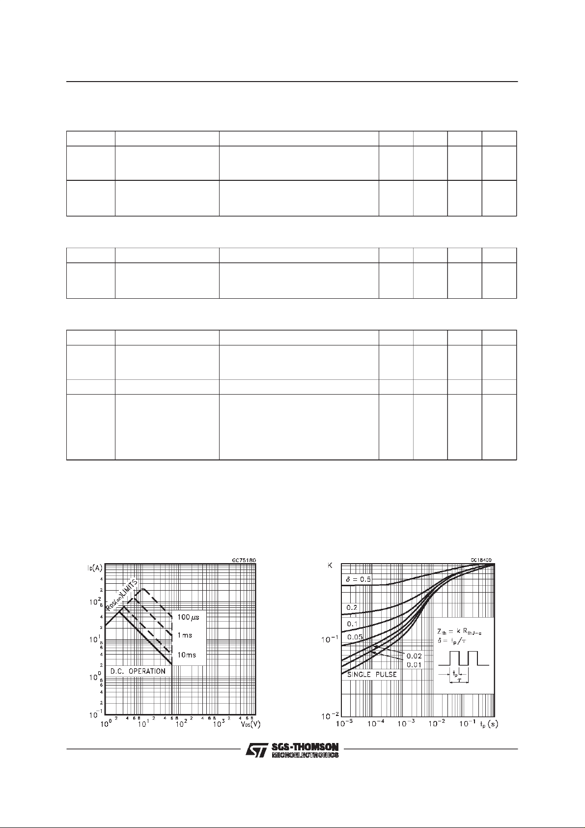
Safe Operating Area ThermalImpedance
3/8
Page 4

STB55NE06
OutputCharacteristics
Transconductance
TransferCharacteristics
StaticDrain-sourceOn Resistance
GateCharge vs Gate-sourceVoltage
4/8
CapacitanceVariations
Page 5

STB55NE06
Normalized Gate ThresholdVoltage vs
Temperature
Source-drainDiode Forward Characteristics
Normalized On Resistance vs Temperature
5/8
Page 6

STB55NE06
Fig. 1: Unclamped InductiveLoad TestCircuit
Fig. 3: SwitchingTimes Test Circuits For
ResistiveLoad
Fig. 2: Unclamped InductiveWaveform
Fig. 4: Gate Charge test Circuit
Fig. 5: Test Circuit For InductiveLoad Switching
And Diode RecoveryTimes
6/8
Page 7

TO-263 (D2PAK) MECHANICAL DATA
STB55NE06
DIM.
MIN. TYP. MAX. MIN. TYP. MAX.
A 4.3 4.6 0.169 0.181
A1 2.49 2.69 0.098 0.106
B 0.7 0.93 0.027 0.036
B2 1.25 1.4 0.049 0.055
C 0.45 0.6 0.017 0.023
C2 1.21 1.36 0.047 0.053
D 8.95 9.35 0.352 0.368
E 10 10.28 0.393 0.404
G 4.88 5.28 0.192 0.208
L 15 15.85 0.590 0.624
L2 1.27 1.4 0.050 0.055
L3 1.4 1.75 0.055 0.068
mm inch
E
A
C2
L2
D
L
L3
B2
B
A1
C
G
P011P6/C
7/8
Page 8

STB55NE06
Information furnished is believed to be accurate and reliable. However, SGS-THOMSONMicroelectronics assumes no responsability for the
consequencesof use of such information nor for any infringement of patents or otherrights of third parties which may resultsfrom its use. No
licenseis granted by implicationor otherwise underany patentor patentrights ofSGS-THOMSONMicroelectronics. Specifications mentioned
in this publicationare subject to change without notice. This publication supersedes and replacesall information previouslysupplied.
SGS-THOMSONMicroelectronics productsarenotauthorizedfor useascriticalcomponents in lifesupportdevices or systems withoutexpress
writtenapproval of SGS-THOMSONMicroelectonics.
1997 SGS-THOMSONMicroelectronics- Printedin Italy - All Rights Reserved
Australia- Brazil - Canada - China - France- Germany - Italy - Japan - Korea - Malaysia - Malta- Morocco - The Netherlands-
Singapore- Spain- Sweden- Switzerland - Taiwan - Thailand - United Kingdom - U.S.A
SGS-THOMSONMicroelectronicsGROUP OF COMPANIES
...
8/8
 Loading...