

Page 1
.
FULLYINTEGRATED DOUBLE SUPERHETERODYNERECEIVER
.
OPERATIONFROM 800MHz TO 1000MHz
.
RECEIVEROUTPUTAS BITSTREAM
.
FULLYINTEGRATEDTRANSMITTER
.
TRANSMITTERINPUT I/Q/REFIQ
OR
I/I, Q/Q
.
INTEGRATEDPOWER AMPLIFIER
.
CT2 PASWITCH-ON PROFILE INTEGRATED
.
VCO’s INTEGRATED
.
SYNTHESIZERSINTEGRATED
.
CHANNELSELECT LOGICON CHIP
.
INTEGRATED VOLTAGEREGULATION
.
SUPPLYVOLTAGESFROM 3.0V TO 5.5V
STB4395
CT2 RECEIVER/TRANSMITTER
ADVANCE DATA
DESCRIPTION
The STB4395(A) is a fully integrated receivertransmitter designed for CT2applications,and incorporatesall the VCO’s, synthesizers,PLLs, and
channel select logic, to make a fully functional
”single chip” radio.
The receiver isof the doublesuperhetarchitecture
and operatesfrom anaerial input (via a SAWfilter)
to bitstreamoutput to CT2 format, whilstthetransmitter operates from I/Q inputs to +13dBm at the
final frequency. A single (external)frequency reference is all that is required to give full coverage
overtherangeof800to1000MHz.Theon-offslope
of theTransmitPAisgovernedinternallytogivethe
required switch-on ramp, whilst the output can be
swiched from low to high power by means of an
externaldigital controlsignal.
Thechannelselectiscontrolled fromadigital serial
input, and allows continuous channel control from
800 to1000MHz.
The STB4395 exists in two versions:
the STB4395, which has
input/outputs, is designed to operate with the
SGS-THOMSON baseband companion part, the
ST5095. TheSTB4395Ahas a 3 wireI/Q interface
and is compatiblewith commercially available I/Q
transmitdata basebandIC’s.
I/I,Q/Q
transmit data
TQFP64
(Plastic Package)
ORDER CODE : STB4395 or STB4395A
April 1996
This is advance informationon a newproduct now in development or undergoingevaluation. Detailsare subject to change without notice.
1/16
Page 2

STB4395
CONTENT Page
1 PIN DESCRIPTION..................................................... 3
1.1 PIN CONNECTIONS. . . . .. . . . . . . . . . . . . . . . . . ............................. 4
1.2 PIN LIST . . . . . . .. . . . . . . . . . . . . . . . . . . . . . . . . ............................. 5
1.3 ANALOGAND FILTERPINS . . . . . . . . . . . . . . . . ............................. 5
1.4 DIGITAL, SIGNALAND CONTROL PINS. . . . . . . . . . .......................... 6
1.5 POWERSUPPLY PINS . ................................................ 6
2 BLOCKDIAGRAM..................................................... 7
3 FUNCTIONAL DESCRIPTION............................................ 8
3.1 RECEIVER . . . . . . . . . . . ................................................ 8
3.2 TRANSMITTER. . . . . ................................................... 8
3.3 CHANNEL SELECTCONTROL LOGIC. . . . .. . . . . . . . . . . . . ................... 8
4 ABSOLUTEMAXIMUM RATINGS......................................... 8
5 POWERSUPPLIES .................................................... 9
5.1 SUPPLIES. . . . . .. . . ................................................... 9
5.2 GROUND PLANECONNECTIONS . ....................................... 9
6 ELECTRICAL CHARACTERISTICS ....................................... 9
7 TIMING INFORMATION................................................. 9
7.1 TURN ON-OFF TIMES . . . . . . . . . . . ....................................... 9
7.2 CHANNEL SELECTTIMING . . . . ......................................... 9
8 TRANSCEIVER SECTION ............................................... 10
8.1 RECEIVER-INPUT SPECIFICATION. . . . . . . . . .. . . . . . . . . .................... 10
8.2 TRANSMITTER OUTPUTSPECIFICATION . .. . . . . .. . . . . .................... 11
8.3 SYNTHESIZER/MODULATOR/CHANNELSELECTLOOP. . . ................... 11
8.3.1 Synthesizerphase noiseand spurious . . . . . . . . .. . . . . . .. . . . . . . . .. . . . . . . . . .. . . 11
8.3.2 Channelselect loop. . . . . . . . .. . . ......................................... 11
8.3.3 Channel frequencysetting . . . . . . . . ....................................... 12
8.4 SYSTEM CLOCKINPUT . . . . . . . . . ....................................... 13
8.5 RECEIVER-RF INPUT. . . . . . . . . . . ....................................... 13
8.6 DIGITALINPUTBUFFERS. . . . . . . . ....................................... 13
8.7 DIGITALOUTPUTBUFFERS. . . . . . ....................................... 13
8.8 RECEIVER-FSH TRI STATE INPUT. . . . . . . . . . . . . . . . ....................... 13
8.9 RECEIVER-RSSI OUTPUT . . . . . . . ....................................... 14
8.10 POWERDOWN BUFFER. . . . . . . . . ....................................... 14
8.11 TRANSMITTER - DATAINPUTS . . . .. . . . . . . . .. . . . . . . . . .................... 14
8.11.1 STB4395A.. . . . . ...................................................... 14
8.11.2 STB4395............................................................. 14
9 APPLICATIONS....................................................... 15
9.1 TYPICALDC CONNECTION SCHEMES. . . . . . . . . . .. . ....................... 15
9.1.1 Internal regulator....................................................... 15
9.1.2 External regulator . . . ................................................... 15
9.2 APPLICATIONCIRCUIT. . . . . . . . . . ....................................... 15
9.2.1 Introduction. . . . . . . .. . . . . . . . . . . . ....................................... 15
9.2.2 Applicationexample . . . . .. . . . . . . . .. . . . . . . . . ............................. 15
10 PACKAGE MECHANICAL DATA ......................................... 16
2/16
Page 3
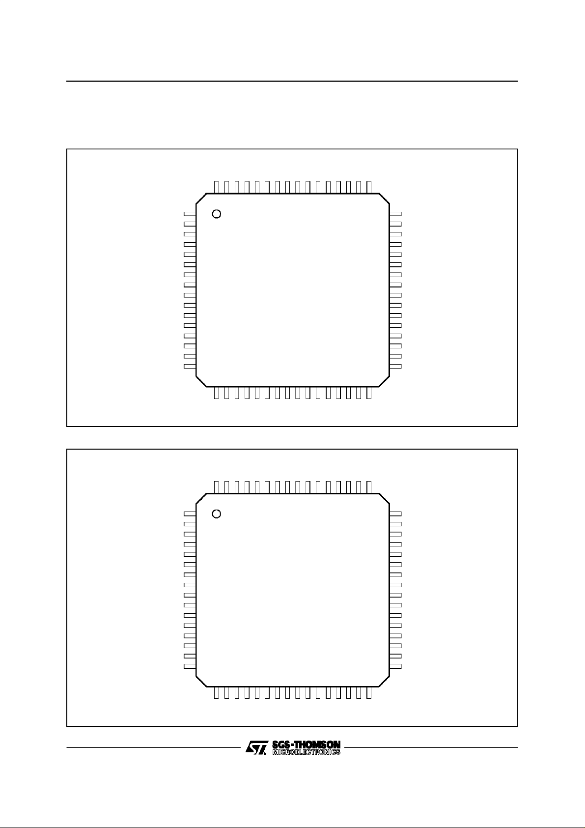
1 - PIN DESCRIPTION
1.1 - Pin Connections
STB4395
STB4395
STB4395A
NPRGEN
PRGCLK
PRGD
NTXEN
LOCK
NQ
EN
VNOSC
VRO
VCOO
NVCOO
FLTRO
VND
64 63 62 61 60 59 58 57 56 55 54 53 52 51 50 49
1
2
3
4
5
6
I
7
NI
8
9
Q
10
11
12
13
14
15
16
17 18 19 20 21 22 23 24 25 26 27 28 29 30 31 32
VPO
VRD
DO
VPD
SLTC
NTXFLT
FSH
ADJPWR
SHAPE
TXFLT
TQFP64
(from above )
VRS
VPS1
FLTRS
RF
VPRF2
VCOS
NVCOS
NRF
VPS2
VPRF1
BRF3
VNPA
BRF1
VRRF
DISCI
NSAWI
SAWI
BRF2
DISCO
VNRF
VPI
48
VNIF
47
SAWO
46
NSAWO
45
VPIF
44
NIF2O
43
IF2O
42
DEC
41
IF2I
40
NIF2I
39
NDEC
38
VRIF
37
RSSISYNCLK
36
VRI
35
VCOI
34
NVCOI
33
FLTRI
4395-01.EPS
NPRGEN
PRGCLK
PRGD
NTXEN
LOCK
REFIQ
EN
VNOSC
VRO
VCOO
NVCOO
FLTRO
FN
VND
64 63 62 61 60 59 58 57 56 55 54 53 52 51 50 49
1
2
3
4
5
6
I
7
8
Q
9
10
11
12
13
14
15
16
17 18 19 20 21 22 23 24 25 26 27 28 29 30 31 32
VPO
VRD
DO
VPD
SLTC
NTXFLT
FSH
ADJPWR
SHAPE
TXFLT
TQFP64
(from above )
VRS
VPS1
FLTRS
RF
VPRF2
VCOS
NVCOS
NRF
VPS2
VPRF1
BRF3
VNPA
BRF1
VRRF
DISCI
NSAWI
SAWI
BRF2
DISCO
VNRF
VPI
48
VNIF
47
SAWO
46
NSAWO
45
VPIF
44
NIF2O
43
IF2O
42
DEC
41
IF2I
40
NIF2I
39
NDEC
38
VRIF
37
RSSISYNCLK
36
VRI
35
VCOI
34
NVCOI
33
FLTRI
4395-02.EPS
3/16
Page 4

STB4395
1 - PIN DESCRIPTION(continued)
1.2 - Pin List
Pin Name Description
1 NPRGEN Serial DataEnable
2 PRGCLK Serial DataClock
3 PRGD Serial Data Input
4 NTXEN Receive-Transmit Switch
5 LOCK VCO Lock Detect-all 3 PLL
6 I I - Transmit Quadrature Input
7 NI I - Transmit Quadrature Input STB4395 only
8 NQ Q-Transmit Quadrature Input STB4395 only
9 Q Q-Transmit QuadratureInput STB4395 only
7 REFIQ IQ Reference QuadratureTransmit Input STB4395A only
8 Q Q-Transmit QuadratureInput STB4395A only
9 FN Forces Data Slicer Reference Time Constant To fast STB4395A only
10 EN Power Down all functions except buffer
11 VNOSC Negative Power Supplyall VCO ’s
12 SYNCLK Synthesizer Clock Input f = 14.4MHz A.C. coupled
13 VRO PSU Regulated Negative Input for TX IF oscillator and pump circuit
14 VCOO TX oscillatortank circuit
15 NVCOO TX Oscillator Tank Circuit
16 FLTRO Loop Filterfor TX PLL
17 VPO Positive Battery Supply for TX oscillator
18 DO Receive Data Output
19 SLTC Slicer Time Constant Capacitor C= 33nF
20 FSH Data Slicer Time Constant Setting
21 FLTRS Loop Filter for channel PLL
22 VRS Regulated Negative Supply for channel oscillator and pump circuit
23 VPS1 Positive Battery Input for channel oscillator and pump circuit
24 NVCOS Channel Oscillator Tank Input 650 to 850MHz
25 VCOS Channel Oscillator Tank Input 650 to 850MHz
26 VPS2 Positive Battery Supply Input for channel oscillator and pump circuit
27 BRF3 Bit Rate Filter3
28 BRF1 Bit Rate Filter1
29 DISCI FM Discriminator Tank Circuit
30 DISCO FM Discriminator Tank Circuit
31 BRF2 Bit Rate Filter 2
32 VPI Positive Battery Supply for RXoscillator and pump circuit
33 FLTRI Loop Filterfor RX oscillator
34 NVCOI RX Oscillator Tank Circuit
35 VCOI RX OscillatorTank Circuit
36 VRI Regulated Negative Supply for RX oscillator and pump circuit
37 RSSI RSSI OUTPUT
38 VRIF Regulated Negative Supply Output forRX sections
39 NDEC RX IF2 Decoupling
40 NIF2I RX IF2 Filter Input
41 IF2I RX IF2 Filter Input
42 DEC RX IF2 Decoupling
43 IF2O RX IF2 Filter Output
44 NIF2O RX IF2 Filter Output
45 VPIF Positive Battery Supply Input for RX sections
Ext. Connectionand
Suppl. Information
4/16
Page 5
STB4395
1 - PIN DESCRIPTION(continued)
1.2 - Pin List (continued)
Pin Name Description Ext. Connection and Suppl. Information
46 NSAWO RX FirstIF Amplifier Input
47 SAWO RX First IF AmplifierInput
48 VNIF Negative Battery Supply Input for RX sections
49 VNRF Negative Battery Supply Input for RF front end
50 SAWI RX First Mixer Output
51 NSAWI RX FirstMixer Output
52 VRRF Regulated Negative Supply for RF front end
53 VNPA Negative Supply for power amplifier
54 VPRF1 Positive Battery Supply for RF front end
55 NRF Input LNA/Output PA
56 RF Input LNA/Ouput PA
57 VPRF2 Positive Battery Supply for RF front end
58 ADJPWR Transmit Power Adjust R = 8.5kΩ to V
59 SHAPE Time Constant for PA on-off ramp C = 560pF
60 TXFLT Bandpass Filter for TX RF
61 NTXFLT Bandpass Filterfor TX RF
62 VPD Positive Battery Supply for digital circuitry
63 VRD Regulated NegativeSupply for digital circuitry
64 VND Negative Battery Supply for digital circuitry
RRF
1.3 - Analog and Filter Pins
Pin Symbol Description
58 ADJPWR Transmitter Output Power Adjust
28 BRF1 Bit RateFilter1
31 BRF2 Bit RateFilter2
27 BRF3 Bit RateFilter3
42, 39 DEC, NDEC RX IF2 Amplifier Decoupling
29 DISCI FM Discriminator Tank Circuit
30 DISCO FM Discriminator Tank Circuit
33 FLTRI Loop Filterfor RX PLL
16 FLTRO Loop Filterfor TX PLL
21 FLTRS Loop Filterfor Channel PLL
6, 7 I, NI(1) Transmit QuadratureInputs ((1)STB4395 only)
40, 41 IF2I, NIF2I Inputs from2nd IF Filter
43, 44 IF2O, NIF2O Outputs to 2nd IF Filter
8, 9 Q, NQ(1) Q-Transmit Quadrature Input ((1)STB4395 only)
7 REFIQ IQ Reference Quadrature Transmit Input (STB4395A only)
56, 55 RF, NRF Input RX LNA/Ouput TX PA
37 RSSI Received SignalStrength Indicator Output
50, 51 SAWI, NSAWI First Mixer Output
47, 46 SAWO, NSAWO First IF Amplifier Input
59 SHAPE Time Constant for PA on-off Ramp
19 SLTC Slicer Time Constant Capacitor
12 SYNCLK Synthesizer Clock Input 14.4MHz
60, 61 TXFLT/ NTXFLT Bandpass Filter for TX RF
35, 34 VCOI, NVCOI Tank Circuit for 152.1MHz RX Oscillator
14, 15 VCOO, NVCOO Tank Circuitfor 300.8MHz TX Oscillator
25, 24 VCOS, NVCOS Tank Circuitfor 650 to 850MHz Channel Oscillator
5/16
Page 6

STB4395
1 - PIN DESCRIPTION(continued)
1.4- Digital,Signal and Control Pins
Pin Symbol Description Polarity
18 DO Receive Data Output
20 FSH Data Slicer Time Constant Setting
9 FN Forces Data Slicer Reference Time Constant
5 LOCK VCO lock detect-all 3 PLL high for LOCK (all three PLL’s)
3 PRGD Serial Synthesizer Data Input, 16 bits word high for logic 1. Input sequence:
1 NPRGEN Serial Synthesizer Data Enable low to enable PRGD buffer
2 PRGCLK Serial Data Clock held high when no clocking,
10 EN Power Down all functions except Enable Buffer high for power up, low for standby
4 NTXEN Receive-Transmit Switch high for receive, low for transmit
(Fast/Slow/Hold)
to fast(STB4395A only)
The time constantof the data slicer is set through the pins FSH and FN for the STB4395Aand through
FSH onlyfor the STB4395(FNinternally connected to High),as listedin the following table :
PIN
High Slow, DO active Fast, DO active
FSH
TriState Fast, DO active Fast, DO active
Low Hold, DO high Fast, DO high
High: slow, tri-state: fast,
low: hold DO goes high on hold (see next table)
low: fast (overides FSH)
high: fast, slow or hold (set by FSH)
LO, D14, D13,...,D0. D14 is the MSB.
LO: logic 1 is low transmit power.
clocks in data on positive edge
FN
High Low
1.5 - Power SupplyPins
Pin Symbol Description
64 VND Negative supply for digital regulators, digital input and output buffers
48 VNIF Negative supply for IF regulators, data output buffer
11 VNOSC Negative supply for the oscillator regulators + substrate
49 VNRF Negative supply RF regulators, quadrature input buffers
53 VNPA Negative supply for PA
62 VPD Positive supply for digital circuitry
32 VPI Positive supply for receive oscillator + charge pump
45 VPIF Positive supply for RX IF + baseband sections
17 VPO Positive supply for transmit oscillator + charge pump
54,57 VPRF1 /VPRF2 Positive supplies for RF front end
23,26 VPS1/VPS2 Positive supplies for ch. select oscillator + charge pump
63 VRD Regulated negative supply for digital circuitry
36 VRI Regulated negative supply for receive oscillator + chargepump
38 VRIF Regulated negative supply for RX IF + baseband sections
13 VRO Regulated negative supply for transmitoscillator + chargepump
52 VRRF Regulated negative supply for RF front end
22 VRS Regulated negative supply ch. select oscillator + charge pump
6/16
Page 7

2 - BLOCKDIAGRAM
Figure1
4NTXEN
Synthesizer
Control
NPRGEN
PRGCLK
PRGD
IQ Input
Data
1
2
3
I
Q
1
1
1
PA/LNA
CONTROL
1
CONTROL
DECODER
IQ Modulator
2
÷
RF S AW
866.05MHz
RF
PA
NRF
1st
LNA
Mixer
SYNTHESIZER
NTXFLT
TXFLT
61 60 56 55 51 50
15
Tx
Mixer
NSAWI
IF S AWLC
150.4MHz
SAWI
2nd Mixer
47
46
44
43
41
40
SAWO
NSAWO
NIF2O
IF2O
IF2I
NIF2I
STB4395
1.7MHz
LC
SYNCLK
14.4MHz
VCO
TANK
PLL
FILTER
VCOO
NVCOO
FLTRO
12
14
15
16
STB4395
DIVIDERS
REFERENCE
Transmit
VCO
300.8MHz
Channel
VCO
716 .45MHz
VCOS
NVCOS
VCO
TANK
Tx
DIVIDER
PHASE
DETECTOR
CHARGE
PUMP
FILTER
PHASE
DETECTOR
CHARGE
PUMP
DATA
SLICER
2124 25 27 28 31 29 30
DO
Data
Out
SLTC
FLTRS
PLL
DIVIDER
PHASE
DETECTOR
CHARGE
PUMP
201918
FSH
Rx
BRF1
BRF3
50kHz
BitRate Filter
FM
Modulator
BRF2
DISCI
DISCO
DEMOD.
TANK
2nd IF Amplifier
Receive
VCO
152.1MHz
37 RSSI
VCOI
35
NVCOI
34
FLTRI
33
VCO
TANK
PLL
FILTER
4395-03.EPS
7/16
Page 8

STB4395
3 - FUNCTIONALDESCRIPTION
Figure 1 is a simplified block diagramof the circuit.
It shows the key on-chip and off-chip functional
blocks and signal paths. For illustration purposes
frequencies have been added representing the
situationwhenreceivingortransmittinga particular
CT2 channel.
3.1 - Receiver
The receivesignalentersthe STB4395viaaninput
SAW filter(866 MHZ for CT2 in Europe).The RF
filter changes the input signal froma singleended
to a balancedsignal,afterwhich thesignal passes
through the LNA, firstmixer, and mixer buffer. The
mixeris drivenbythechannel VCO,whichis inturn
controlledby the synthesizer.
The signal path continues via the first IF SAW
(150.4MHz),IF amplifierto the second mixer. The
second mixer stage mixes down to 1.7MHz, and
via anexternalLC IF filter,ispassed to the second
IF amplifier, where the main system gain takes
place. The RSSI output is available from this
point.The signal is then demodulated and sliced
into adata streamwhich is the binarydigital output
availableto the base band chip.
The channelselectionisprovidedbythe two external filters:the first IF SAW and a secondIF 2-pole
LC filter.
3.2 - Transmitter
The chip accepts 72Kbits/s data in an I/Q format.
The I/Qinputs pass via the I/Q modulator to the
TX mixer. The TX mixer is driven by the same
channelVCO as the receive first mixer.
Theon-offrampofthetransmit PA.iscontrolledvia
an external capacitor to give minimum spurious
responseswhenswitchingon and off.
The PA output power can be switched from full
power to -3dBm by the channel select control
signal(bit LOof the 16bits serial word PRGD, see
table,paragraph 1.4).
3.3 - Channel Select Control Logic
All channel phase locked loops and oscillatorsare
included on chip. The channel control synthesizer
is controlledexternallyvia a 3 wire interface.
The Reference clock input of 14.4 MHz is divided
using preset counters to set the phase detector
/charge pump loops for the synthesizer/channel
select VCO,the secondreceiverVCO,and theI/Q
transmit VCO. The phase detector inputs for the
fixedfrequency VCO’sareviapresetdividersalso.
Thechannelselectcontroland TransmitPAcontrol
is viaa 16bitserialword,whichisgeneratedbythe
system controller. 15 bits of this serial word are
used for the channelinformation,and 1 bit isused
to settheoutputpowerofthetransmitPA.Theword
length is sufficient to give full channel coverage
over the range from 800 to 1000MHz with integer
multiples of 50KHz. The section ”system clock
input” gives a detaileddescription.
Not shown in the diagramare the voltageregulatorsforthe receiveLNA/firstmixer,TransmitPA,TX
mixerand the remainder of the circuit.Thereare 6
internal voltageregulators to ensure the minimum
of mutualinterference.
4 - ABSOLUTEMAXIMUM RATINGS
Symbol Parameter Value Unit
Power Supply Voltage 7.0 V
Voltages on Input (except SYNCLK) 5.9 V
Voltage on Input (SYNCLK) 3.0 V
Voltages on Input 7.0 V
Voltages on Output 7.0 V
Voltages on Output 7.0 V
Voltage Out of RF or NRF in TX 3.5 V
Storage Temperature 125
Operating Temperature 40
V
8/16
V
P-VN
V
P-VIN
V
P-VIN
V
IN-VN
V
P-VOUT
N-VOUT
V
RFO
T
stg
T
oper
PP
o
C
o
C
Page 9

STB4395
5 - POWERSUPPLIES
5.1 - Supplies
The chip operates from a power supply of 3.0 to
5.5 Volts. All interface circuits to the baseband
chipsare operatedbetween these supplies.
Six on-chip regulators are included on-chip which
provide toallpartsof the circuitseparateregulated
voltagesupplies of -2.85±0.15 Voltsrelativetothe
top railfortheRFcircuitry, theIFcircuitry,thedigital
circuitry and forthe threeVCO’s.
The chipcanbe operatedin 3 modes,powerdown,
receiveandtransmit.Power down is activated taking the Pin EN to V
mode, NTXEN is takento V
. To transfer to the receive
N
.
P
The built-in regulators can be by-passed ,if so
required.
positivesupply, V
strongly recommended that the chip be mounted
on a boardwith a ground plane connected to V
Becausethe base band chip isspecifiedrelativeto
a negativeground, it is further recommendedthat
the board used is a 4 layer board with both a
positive,V
, and negative ground plane VN. This
P
has the additional advantage of providing good
high frequencydecoupling betweensupplies.
The questionas to whetherto call V
depends on which external equipment is connected. For testing the baseband section, this is
; for testing the radio chip, this is VP.Ina
V
N
product, this will dependon the application.
For clarity all voltages specified in this document
,at manypoints. Thereforeit is
P
or VNground
P
will be specified with respect to the supply, V
5.2 - Ground Plane Connections
The chiphasbeen designedto bedecoupledtothe
,that thevoltagenormallytracks with whenthe
V
N
supplyis varied.
6 - ELECTRICAL CHARACTERISTICS
Symbol Parameter Min. Typ. Max. Unit
V
V
REG
IRX Receive Mode 32 40 mA
ITX Transmit Mode 68 80 mA
IQ Standby/Power Down 20 µA
Power Supply Voltage (unregulated) -3 -5.5 V
N
Power Supply bypassing Internal Regulators (this is alsointerface supply) -2.7 -3 V
.
P
or
P
7 - TIMING INFORMATION
7.1 - Turn on-off Times
Timesare relative to theNTXEN transition(high to lowfor receiveto transmitand low tohigh for transmit
to receive).
Symbol Parameter Min. Typ. Max. Unit
t
ON
t
RAMPON
t
TXRX
Turn-on Time From standby to receive 10 µs
PA Power Ramp up to reach -3dB of final power 27.78 µs
Switchover Time Transmit to Receive (LNA/first mixeractive) 27.78 µs
7.2 - Channel Select Timing
PRGCLKmust be high beforeNPRGENgoes low to programmethe synthesizer.
Figure 2 : Timingof Serial Programming Data
Order of NPRGEN &PRGD unimportant
NPRGEN
PRGCLK
PRGD
PROGRAM
CODE
Code cha nges on Rising Edge ofNPRGEN
Note thatalthoughanewprogramcodeisimplementedon the risingedgeofthe NPRGEN,thetransmitted
power level is delayeduntil at the start of thenext burst of transmission.In order to change transmitpower
during a conversation,the required power code must beseriallyloaded with the power change instruction.
4395-04.EPS
9/16
Page 10

STB4395
8 - TRANSCEIVERSECTION
Symbol Description Min. Typ. Max. Unit
f
OP
P
OUTTX
8.1 - Receiver-InputSpecification
LNA, firstmixer and buffer
Symbol Parameter Min. Typ. Max. Unit
Frequency Range 800 1000 MHz
Channel Frequency Accuracy -1 0 1 kHz
Modulation Deviation (synchronised with72 Kbits/s data rate) 18 kHz
Output Power (300Ω balanced)high power mode 13 dBm
Sensitivity (source 300Ωbalanced) for1E-3 BER -103 -105 dBm
Signal max. for1E-3 BER 0 dBm
Conversion voltage gain 33.7 ± 1.5 dB
Available conversion powergain 21.5 ± 1.5 dB
Input impedance 300Ω //3pF Output impedance 5kΩ // 3pF Source impedance 300Ω //-3pF Load impedance 5kΩ // -3pF Noise figure 3.5 dB
1dB compression point(input) -24 dBm
Third order intercept (input) -14 dBm
First IFamplifier, second mixer and buffer
Symbol Parameter Min. Typ. Max. Units
Conversion Voltage Gain 22.0 ± 1.5 dB
Available Conversion PowerGain 16.3 ± 1.5 dB
Input Impedance 700Ω // 2pF Output Impedance 2kΩ // 2pF Source Impedance 700Ω // -2pF Load Impedance 2.8kΩ // -2pF Noise Figure 6 dB
1dB Compression Point (input) -32 dBm
Third Order Intercept (input) -22 dBm
Second IF amplifier
Symbol Parameter Min. Typ. Max. Unit
Conversion Voltage Gain 82 ± 3dB
Available Power Gain (to DISCO) 86 ± 3dB
Bandwith (3dB) 3 MHz
Input Impedance 10kΩ //pF Output Impedance (to DISCO) 1.1kΩ // 2F Source Impedance 2.2kΩ // -2pF Load Impedance (at DISCO) see App. Diag.
Noise Figure 6 dB
1dB Compression Point (input) -108 dBm
10/16
Page 11

STB4395
8 - TRANSCEIVERSECTION (continued)
Dataslicertime constants
Symbol Parameter Min. Typ. Max. Unit
Slow 3* ms
Fast 130* µs
Hold Drift Rate60mV < signal< 100mV 1 mV/ms
For 33nF capacitorat SLTC
8.2 - Transmitter-Output Specification
Symbol Parameter Min. Typ. Max. Unit
P
OUT
TXFLT/NTXFLT output
Symbol Parameter Min. Typ. Max. Units
Output Power into300Ω balanced, high powermode 13 dBm
LO Rejection 25 dBC
Output Control Switch 14 dB
Output Impedance 2 kΩ
Load Impedance (external) 1.2 kΩ
Voltage Out (channel frequency,application circuit of this D/S) 200 mV
Voltage Out (channel frequency-300.8MHz, app. cct of this D/S) 80 mV
PP
PP
8.3 - Synthesizer/Modulator/ChannelSelect Loop
8.3.1 - SynthesizerPhase Noise and Spurious
Phasenoise and spuriousare measuredat the RF outputs RF / NRF in transmitmode, no RF SAWfilter.
Phase Noise (Average)
Offset Frequency from carrier Min. Typ. Max. Unit
±100kHz -106 dBc/Hz
±500kHz -121 dBc/Hz
±1MHz -127 dBc/Hz
±10MHz -145 dBc/Hz
Spurious
Offset Frequency from carrier Min. Typ. Max. Unit
±50kHz -55 dBc
±100kHz -63 dBc
±200kHz -70 dBc
±200kHz to ±10MHz -75 dBc
±10MHz to ±100MHz -40 dBc
8.3.2 - ChannelSelect Loop
Symbol Parameter Min. Typ. Max. Unit
Frequency channel - 150.4 MHz
Frequency Steps 50 kHz
11/16
Page 12

STB4395
8 - TRANSCEIVERSECTION (continued)
8.3.3 - ChannelFrequency Setting
8.3.3.1 - GeneralCase
Using, from the divider ratios : andfrom the mixers :
F
=CH*FX/288 F
CH
FRX= RX *FX/16 F
F
= 0.5 *F
IFTX
FTX=TX*F
SYN
TX
/18
the RFfrequencyis related to the other frequenciesby :
F
RF
=FCH+F
=F
CH+FRX-FIF2
IFTX
=CH*F
=CH*F
Hence the channelselect input(15 of the 16 digits, see pin table, paragraph 1.4) serialdata stream :
CH = (F
RF
- TX*F
/18*0.5 ) * 288/F
SYN
where :
F
is the channelPLLsynthesizer frequency
CH
is the firstif frequency(receive)
F
IF1
is the secondif frequency(receive)
F
IF2
F
is thetransmitif frequency
IFTX
is the desiredrf frequency
F
RF
is thereceiveoffset PLL frequency
F
RX
isthe referenceinput frequency(on SYNCLK)
F
SYN
is thetransmitoffset PLLfrequency
F
TX
RX isthe fixed receive divide ratio of 169
TX is the fixed transmit divide ratioof 376
CH isthe channel synthesizerdivide ratiodefinedby the binary channel number,
e.g. D14,D13,...........D0
The channel synthesizer provides integral division for all numbers between 3968 and 32764 (binary
000111110000000to 1111111 11111100).Binary numbers outside this range will cause division ratios not
directly related to binarycode.
IF2=FRX-FIF1
IF1=FRF-FCH
FRF=FCH+F
/288 + TX * F
SYN
/288 + RX* F
SYN
=288* FRF/F
SYN
IFTX
SYN
SYN
SYN
/18 * 0.5
/16 -F
IF2
-3008 and CH = 288 (FRF+F
IF2
)/F
SYN
-3042
8.3.3.2 - ParticularCase. withF
F
= 152.1MHz
RX
=300.8MHz
F
TX
F
= 150.4MHz
IFTX
=150.4MHz
F
IF1
=1.7MHz
F
IF2
Then CH= 20 * F
RF
- 3008
Example: desiredRF frequency,F
= 14.4MHz :
SYN
=866.05MHz
RF
Then substitutingin : CH = 20*866.05-3008= 14313 (binary 011011111101001)
12/16
Page 13

STB4395
8 - TRANSCEIVERSECTION (continued)
8.4 - System Clock Input
Symbol Description Min. Typ. Max. Unit
(*1) Reference Frequency 14.4 MHz
f
REF
V
S
I
IH
I
IL
(*1) limits according to ETSI specification
Input Voltage Swing, AC Coupled, referenced to V
P
Input Current-High (with respect to VN) -40 µA
Input Current-low (with respect to VN)40µA
8.5 - RF/NRFReceive/TransmitPins
Symbol Description Min. Typ. Max. Unit
Z
IN
Input Impedance (balanced, RX) 300Ω // 3.5pF -
VSWR VSWR 1.5:1 -
V
IN DC Max.
P
IN AC Max.
Z
OUT
DC Input Voltage 0V
AC Input Power 0 dBm
Output Impedance (balanced, TX) 300Ω //3pF -
8.6 - Digital Input Buffers NTXEN, PRGD, NPRGEN, PRGCLK, FN
Symbol Description Min. Typ. Max. Unit
V
IH
V
IL
I
IH
I
IL
Tt Input Edge Transition 0.1 1 µs/V
Upper Level Input Voltage VP-1 VP+0.4 V
Lower Level Input Voltage VN-0.4 VN+1 V
Input Current High -10 µA
Input Current Low 40 µA
0.4 0.8 V
8.7 - Digital Output Buffers xLOCK, DO
Symbol Description Min. Typ. Max. Unit
V
OH
V
OL
t
R
t
F
Upper Level Output Voltage VP-0.3 V
Lower Level Output Voltage V
N
P
VN+1 V
Rise Time (load of 5pF) 0.3 µs/V
Fall Time (load of 5pF) 0.4 µs/V
8.8 - Receiver - FSHTri State Input
Symbol Description Min. Typ. Max. Units
V
IH
V
IL
I
TR
I
IH
II
L
T
Upper Level Input Voltage VP-0.3 VP+0.4 V
Lower Level Input Voltage VN-0.4 VN+1 V
Tri State Current -10 10 µA
Input Current High -100 µA
Input Current Low 100 µA
Input Edge Transition 0.1 1 µs/V
t
V
13/16
Page 14

STB4395
8 - TRANSCEIVERSECTION (continued)
8.9 - Receiver-RSSIOutput
The receiver output swingsbetweenV
connectedto V
Symbol Description Min. Typ. Max. Unit
P
MIN
P
MAX
R
OUT
V
MIN
V
MAX
CF conversion factor -200 mV/decade
. The output has to besmoothed externallywith a capacitorto VN.
N
Min RF Input Power Registered -90 dBm
Max RF Input Power Registered -44 dBm
Output Resistance (internallyconnected to VN)50kΩ
Voltage for P
Voltage for P
MIN
MAX
8.10 - PowerDown Buffer, EN
Symbol Description Min. Typ. Max. Unit
V
IH
V
IL
I
IH
I
IL
t
ON
tO
FF
(1) assumes application circuit with 100nF on each regulator.
Upper Level Input Voltage VP-0.3 VP+0.4 V
Lower Level Input Voltage VN-0.4 VN+0.3 V
Input Current High -350 µA
Input Current Low 10 µA
Buffer Delay to LOCK HI (1) 10 ms
Buffer Delay to min Supply Current (1) 10 ms
andVN.The bufferoutputsupplies acurrent to an on-chipresistor
P
VN+1.25 VN+2 V
V
VN+0.25 V
N
8.11- Transmitter-DataInputs
8.11.1- I,Q,REFIQ(STB4395A)
Symbol Description Min. Typ. Max. Units
R
EXT
R
INT
R
IM
V
DC
V
DC match
V
S
V
S match
External Input Resistance 6.5 6.8 7 kΩ
Internal Input Resistance 32 40 50 kΩ
R
Matching Error 1 %
INT
DC Bias to R
EXT
VDCMatching Error to R
Peak Voltage Swing to R
VSMatching Error to R
EXT
EXT
EXT
0.96VHS 1.04VHS V
5mV
0.45 0.5 0.56 V
0.5 dB
Phase(I-Q) 88.5 90 91.5 degrees
VHS = (VP+VN)/2
8.11.2- I,Q,NI,NQ (STB4395)
VHS = (V
Symbol Description Min. Typ. Max. Unit
R
EXT
R
INT
R
IM
V
DC
V
DC match
V
S
V
S match
)/2 - VHR = (VP+VRD)/2
P+VN
External Input Resistance 2 kΩ
Internal Input Resistance 32 40 50 kΩ
R
Matching Error 1 %
INT
DC bias to R
EXT
VDCMatching Error to R
Peak Voltage Swing to R
VSMatching Error to R
EXT
EXT
EXT
VHS-0.7 VHR+0.7 V
12 mV
0.7 0.75 0.85 V
20 mV
Phase (I/Ibar and Q/Qbar) 88.5 90 91.5 degrees
Phase I to Ibaror Q to Qbar 0 degrees
14/16
Page 15

9 - APPLICATIONS
9.1 - TypicalDC connectionschemes
9.1.1 - InternalRegulator
The STB4395has built-ininternalregulatorswhich
allows 15mAto be used for externalcircuitry.The
output ofthisregulatoris -2.85Vwithrespectto the
positivesupply rail.
9.1.2 - ExternalRegulator
The STB4395will always generate its own supply
voltage(-2.85V with respect to V
), but the I/O
P
interfaces allow the STB4395 to swing its output
levelsto thesupplyrails(V
toVN).Thesystemand
P
baseband controller can therefore be connected
from the same -unregulated- supply and be individuallyregulated, if required .
9.2 - ApplicationCircuits
9.2.1 - Introduction
The STB4395makes use of some unusual circuit
Figure3
STB4395
configurations:
- The STB4395operatesfrom positiveground.The
decoupling of the supply lines should take into
account that the a.c. groundconnectionswill be
reversed with respect to the baseband circuit
and/or the microcontroller. The use of multilayer
PCB is recommended.
- The filters have been adapted for the best performance of the IC, although standardconfigurations are also considered.
9.2.2 - FullyConfigured Applications Example
Figure 3 is a typical application circuit for a complete system. It shows the typical external components to the circuit. As the reactance of the
componentsis criticalin many locations,the use of
surfacemountedcomponentsis essential.Atypical
component list is also attached.It also showsthe
typicalvalues for the thevarious VCO circuits.The
valuesare very dependenton layout.
NVBAT
NPRGE N
PRGCLK
PRGD
NTXEN
LOCK
REFIQ
RSSI
VRD
FSH
50Ω
SAW
866MHz
300
Ω
R18
R15 2kΩ
VP
C3
C6
100nFC9100 nF
10µF
L1 330 µH
C1
56pFC456pFC756p F
R1 2k
Ω
R2 2k
Ω
R4 2k
I
R3 0Ω
Q
FN
EN
DO
R6 0Ω
R5 0Ω
R9 6.8 kΩ
C8
C5
C2
0pF
SYNCLK
0pF
0pF
51Ω
C16, C15, C19, C21 ,C 23, C41, C45
provision for conn ection to grou nda lso
300pF
C11
10n F
R8
R12 50
R10 6. 8kΩ
C12
300pF
L3 1 5nH
Ω
L2 1 5nH
VN
VN
L4
C10
56µH
56pF
Ω
R7 2k
Ω
R11 6. 8kΩ
C13
C14
300pF
C17
100 nF
R13
5.1k
Ω
C15
82n F
C18 20 0nF
C16
2-6p F
C19
8.2 nF
1
2
3
4
5
6
7
8
9
10
11
12
13
14
15
16
C24 0pF
C22
100nF
VN
17 18 19 20 26 2 7 28 2 9 30
R14
5.1k
Ω
C21
47nF
C26
L5
560pF
8.2nH
21 22 23 24 31 32
C20
33nF
C23
4.7 pF
C25
100nF
Approx value s ofb uried track
5Ω
L8
L7
8nH
10nH
R16 4 .7kΩ
STB4395A
TQFP64
(from above)
25
C27
L9
L6
0pF
8nH
8nH
R17
20
Ω
indu ctance s togrou nd
68p F
L10
L11
8nH
10n H
0-10k
C29
100nF
C28
R19
27k
Ω
R20
27k
Ω
L14 750 nH
L16 270 nH
R21
C28
68pF
R23
20Ω
Ω
L15 270 nH
L13 750 nH
VNVN
50
4956575860 51525354555961626364
48
47
46
45
44
43
42
41
2-50 pF
40
39
38
37
36
35
34
33
R22
10kΩ
C34
10nF
C33
C32
VN
C41
100nF
5.6nF
L12
56µH
SAW
150.4MHz
L19
1200nH
C43
1nF
C45
820pF
1kΩ
1k
Ω
L17 47 nH
L18 47 nH
R24
5.1k
C40
56nF
L21 3 90nH
L20 3 90nH
C44
820pF
Ω
C39
2-50 pF
100
and 2pF
Ω
700
47pF
R25
C48
R26
10kΩ
Ω
C46
100nF
L23
10µH
C49
47pF
L22
10µH
C47
100 nF
VN
and 2pF
Ω
700
C42
2-50p F
10n F
10n F
C38
C37
2-6p F
C36
C31
20pF
C35
100p F
4395-05.EPS
15/16
Page 16

STB4395
PACKAGE MECHANICALDATA
64 PINS- PLASTICQUADFLATPACK(THIN)
D
D1
49
A
A2
A1
3348
32
0.10mm
Seating Plane
B
C
Dimensions
B
64
1
e
TQFP64
E3D3E1
17
16
E
L1
L
K
Millimeters Inches
Min. Typ. Max. Min. Typ. Max.
A 1.60 0.063
A1 0.05 0.15 0.002 0.006
A2 1.35 1.40 1.45 0.053 0.055 0.057
B 0.18 0.23 0.28 0.007 0.009 0.011
C 0.12 0.16 0.20 0.0047 0.0063 0.0079
D 12.00 0.472
D1 10.00 0.394
D3 7.50 0.295
e 0.50 0.0197
E 12.00 0.472
E1 10.00 1 0.394
E3 7.50 0.295
K0
o
(Min.), 7o(Max.)
L 0.40 0.60 0.75 0.0157 0.0236 0.0295
L1 1.00 0.0393
Information furnished is believed to be accurate and reliable. However, SGS-THOMSON Microelectronicsassumes no responsibility
for the consequences of use of such information nor for any infringement of patents or otherrights of third parties which may result
from its use. Nolicence is granted by implication or otherwise underany patent or patentrights of SGS-THOMSON Microelectronics.
Specifications mentioned in this publication are subject to change without notice. This publication supersedes and replaces all
information previously supplied. SGS-THOMSON Microelectronics products are not authorized for use as critical components in life
support devices or systems without express written approval of SGS-THOMSON Microelectronics.
PMTQFP64.EPS
TQFP64.TBL
16/16
1996 SGS-THOMSON Microelectronics - All RightsReserved
Purchase of I2C Components of SGS-THOMSON Microelectronics, conveys a license under the Philips
2
I
C Patent. Rights to use these components in a I2C system, is granted provided that the system conformsto
2
the I
C Standard Specifications as defined by Philips.
SGS-THOMSON Microelectronics GROUP OF COMPANIES
Australia - Brazil - China- France - Germany - Hong Kong - Italy - Japan- Korea - Malaysia - Malta - Morocco
The Netherlands - Singapore - Spain - Sweden - Switzerland - Taiwan - Thailand - United Kingdom - U.S.A.
 Loading...