

Page 1
STB40NS15
N-CHANNEL 150V - 0.042Ω - 40A D2PAK
MESH OVERLAY™ MOSFET
PRELIMINARY DATA
TYPE V
DSS
R
DS(on)
I
D
STB40NS15 150 V <0.052Ω 40A
■ TYPICAL R
■ EXTREMELY HIGH dv /d t C APABILITY
■ VERY LOW INTRINSIC C APAC ITANCES
■ GATE CHARGE MINIMIZED
(on) = 0.042Ω
DS
DESCRIPTION
This powermos MOSFET is designed using the
company’s consolidated strip layout-based MESH
OVERLAY
™ process. This technology matches
and improves the performances compared with
standard parts from various sources.
APPLICATIONS
■ HIGH CURRENT SWITCHING
■ UNINTERRUPTIBLE POWER SUPPLY (UPS)
■ PRIMARYSWITCH IN ISOLATED DC-DC
CONVERTERS
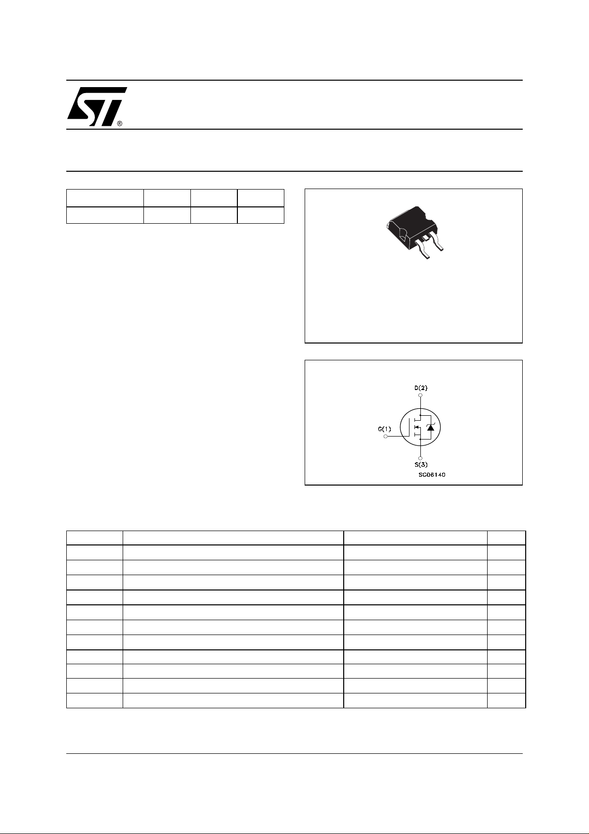
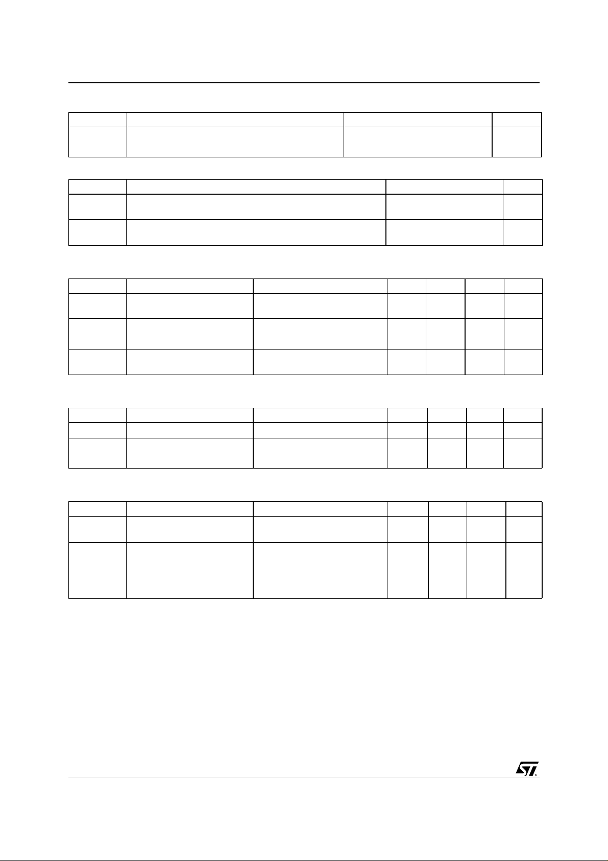
3
1
D2PAK
I
NTERNAL SCHEMATIC DIAGRAM
ABSOLUTE MAXIMUM RATINGS
Symbol Parameter Value Unit
V
DS
V
DGR
V
GS
I
D
I
D
I
DM
P
TOT
dv/dt Peak Diode Recovery voltage slope 9 V/ns
T
stg
T
j
(•)Pu l se width limited by safe operating area
December 2001
This is preliminary information on a new product now in development or undergoing evaluation. Details are subject to change without notice.
Drain-source Voltage (VGS = 0)
Drain-gate Voltage (RGS = 20 kΩ)
150 V
150 V
Gate- source Voltage ±20 V
Drain Current (continuos) at TC = 25°C
Drain Current (continuos) at TC = 100°C
(●)
Drain Current (pulsed) 160 A
Total Dissipation at TC = 25°C
40 A
25 A
140 W
Derating Factor 0.933 W/°C
Storage Temperature –65 to 175 °C
Max. Operating Junction Temperature 175 °C
1/7
Page 2
STB40NS15
THERMA L D ATA
Rthj-case Thermal Resistance Junction-case Max 1.07 °C/W
Rthj-amb Thermal Resistance Junction-ambient Max 62.5 °C/W
T
l
AVALANCHE CHARACTERISTICS
Symbol Parameter Max Value Unit
I
AR
E
AS
ELECTRICAL CHARACTERISTICS (TCASE = 25 °C UNLESS OTHERWISE SPECIFIED)
OFF
Symbol Parameter Test Conditions Min. Typ. Max. Unit
V
(BR)DSS
I
DSS
I
GSS
Maximum Lead Temperature For Soldering Purpose 300 °C
Avalanche Current, Repetitive or Not-Repetitive
(pulse width limited by T
max)
j
Single Pulse Avalanche Energy
(starting T
Drain-source
= 25 °C, ID = IAR, VDD = 50 V)
j
ID = 250 µA, VGS = 0 150 V
40 A
500 mJ
Breakdown Voltage
Zero Gate Voltage
Drain Current (V
GS
Gate-body Leakage
Current (V
DS
= 0)
= 0)
V
= Max Rating
DS
V
= Max Rating, TC = 125 °C
DS
V
= ±20V ±100 nA
GS
1µA
10 µA
ON
(1)
Symbol Parameter Test Conditions Min. Typ. Max. Unit
V
GS(th)
R
DS(on)
Gate Threshold Voltage
Static Drain-source On
V
= VGS, ID = 250µA
DS
VGS = 10V, ID = 40 A
234V
0.044 0.052 Ω
Resistance
DYNAMIC
Symbol Parameter Test Conditions Min. Typ. Max. Unit
(1) Forward Transconductance VDS > I
g
fs
C
iss
C
oss
C
rss
Input Capacitance
Output Capacitance 380 pF
Reverse Transfer
Capacitance
I
D
V
= 20A
DS
D(on)
x R
DS(on)max,
= 25V, f = 1 MHz, VGS = 0
20 S
2400 pF
160 pF
2/7
Page 3
STB40NS15
ELECTRICAL CHARACTERISTICS (CONTINUED)
SWITCHING ON
Symbol Parameter Test Conditions Min. Typ. Max. Unit
t
d(on)
t
r
Q
Q
gs
Q
gd
g
Turn-on Delay Time
Rise Time
Total Gate Charge VDD = 120V, ID = 40A,
Gate-Source Charge 17 nC
Gate-Drain Charge 47 nC
SWITCHING OFF
Symbol Parameter Test Conditions Min. Typ. Max. Unit
t
d(off)
T
t
r(Voff)
t
t
f
f
c
Turn-off Delay Time
Fall Time
Off-voltage Rise Time
Fall Time
Cross-over Time
= 75V, ID = 20A
V
DD
RG= 4.7Ω, VGS = 10V
(see test circuit, Figure 3)
VGS = 10V
V
= 75V, ID = 20A
DD
R
=4.7Ω, VGS = 10V
G
(see test circuit, Figure 3)
V
= 120V, ID = 20 A,
clamp
RG=4.7Ω, V
GS
= 10V
(see test circuit, Figure 5)
25 ns
45 ns
100 110 nC
85 ns
47
35
70
ns
ns
ns
SOURCE DRAIN DIODE
Symbol Parameter Test Conditions Min. Typ. Max. Unit
I
SD
I
SDM
V
(1)
SD
t
rr
Q
rr
I
RRM
Note: 1. Pulsed: Pu l se duration = 300 µs, duty c yc l e 1.5 %.
2. Pulse width li mited by safe operating area.
Source-drain Current 40 A
(2)
Source-drain Current (pulsed) 160 A
Forward On Voltage
Reverse Recovery Time
Reverse Recovery Charge
Reverse Recovery Current
ISD = 40A, VGS = 0
= 40A, di/dt = 100A/µs,
I
SD
VDD = 50V, Tj = 150°C
(see test circuit, Figure 5)
270
200
1.5
1.5 V
ns
nC
A
3/7
Page 4

STB40NS15
Fig. 2: Unclamped Inductive WaveformFig. 1: Unclamped Inductive Load Test Circuit
Fig. 3: Switching Times Test Circuit For
Resistive Load
Fig. 5: Test Circuit For Inductive Load Switching
And Diode Recovery Times
Fig. 4: Gate Charge test Circuit
4/7
Page 5

2
D
PAK MECHANICAL DATA
STB40NS15
DIM.
MIN. TYP MAX. MIN. TYP. MAX.
A 4.4 4.6 0.173 0.181
A1 2.49 2.69 0.098 0.106
A2 0.03 0.23 0.001 0.009
B 0.7 0.93 0.027 0.036
B2 1.14 1.7 0.044 0.067
C 0.45 0.6 0.017 0.023
C2 1.23 1.36 0.048 0.053
D 8.95 9.35 0.352 0.368
D1 8 0.315
E 10 10.4 0.393
E1 8.5 0.334
G 4.88 5.28 0.192 0.208
L 15 15.85 0.590 0.625
L2 1.27 1.4 0.050 0.055
L3 1.4 1.75 0.055 0.068
mm. inch
M 2.4 3.2 0.094 0.126
R 0.4 0.015
V2 0º8º
3
5/7
1
Page 6

STB40NS15
D2PAK FOOTPRIN T
TAPE AND REEL SHIPMENT (suffix ”T4”)*
TUBE SHIPMENT (no suffix)*
REEL MECHANICAL DATA
DIM.
A 330 12.992
B 1.5 0.059
C 12.8 13.2 0.504 0.520
D 20.2 0795
G 24.4 26.4 0.960 1.039
N 100 3.937
T 30.4 1.197
mm inch
MIN. MAX. MIN. MAX.
TAPE MECHANICAL DATA
DIM.
A0 10.5 10.7 0.413 0.421
B0 15.7 15.9 0.618 0.626
D 1.5 1.6 0.059 0.063
D1 1.59 1.61 0.062 0.063
E 1.65 1.85 0.065 0.073
F 11.4 11.6 0.449 0.456
K0 4.8 5.0 0.189 0.197
P0 3.9 4.1 0.153 0.161
P1 11.9 12.1 0.468 0.476
P2 1.9 2.1 0.075 0.082
R 50 1.574
T 0.25 0.35 0.0098 0.0137
W 23.7 24.3 0.933 0.956
* on sales type
6/7
mm inch
MIN. MAX. MIN. MAX.
BASE QTY BULK QTY
1000 1000
Page 7

STB40NS15
Information furnished is believed to be accurate and reliable. However, STMicroelectronics assumes no responsibility for the consequences
of use of such informa tion n or for an y infring ement of patent s or other rig hts of third part ies which may resu lt from its use . No l i cen se i s
granted by implication or otherwise under any patent or patent rights of STMicroelectronics. Specification mentioned in this publication are
subject to change without notice. This publication supersedes and replaces all information previously supplied. STMicroelectronics products
are not authorized for use as critical compo nents in life support devices or systems without express written approval of STMicroelectronics.
Australia - Brazil - China - Finland - France - Germany - Hong Kong - India - Italy - Japan - Malaysia - Malta - Morocco -
The ST logo is a trademark of STMicroelectronics
© 2001 STMicroelectronics – Printed in Italy – All Rights Reserved
STMicroelectronics GROUP OF COMPANIES
Singapore - Spain - Sweden - Switzerland - United Kingdom - U.S.A.
http://www.st.com
7/7
 Loading...