

Page 1
STB40NF10L
N-CHANNEL 100V - 0.028Ω - 40A D2PAK
LOW GATE CHARGE STripFET™ POWER MOSFET
TYPE V
DSS
STB40NF10L 100 V < 0.033
■ TYPICAL R
■ EXCEPTIONA L dv/d t CAPABILITY
■ 100% AVALANCHE TESTED
■ APPLICATION ORIENTED
(on) = 0.028Ω
DS
R
DS(on)
I
D
Ω
40 A
CHARACTERIZATION
■ ADD SUFFIX “T4” FOR ORDERING IN TAPE &
REEL
DESCRIPTION
This Power Mosfet series realized with STMicroelectronics unique STripFET process has specifically been designed to minimize input capacitance and
gate charge. It is therefore suitable as primary
switch in advanced high-efficiency isolated D C-DC
converters for T el ecom and Computer application. It
is also intended for any application with low gate
charge drive requirements.
APPLICATIONS
■ HIGH-EFFICIENCY DC-DC CONVERTERS
■ UPS AND MOTOR CONTROL
■ AUTOMOTIVE
3
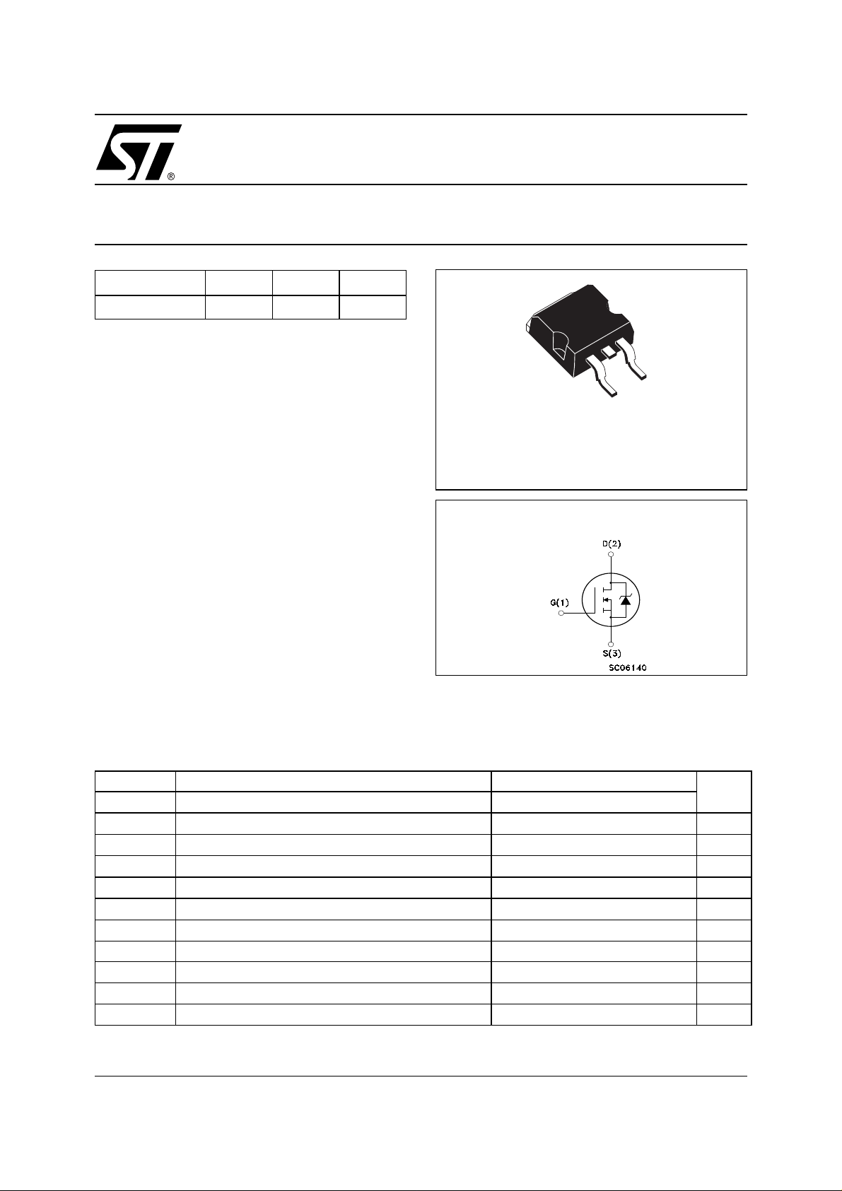
1
D2PAK
INTERNAL SCHEMATIC DIAGRAM
ABSOLUTE MAXIMUM RATINGS
Symbol Parameter Value Unit
V
DS
V
DGR
V
GS
I
D
I
D
I
DM
P
TOT
E
AS
T
stg
T
j
(●) Pulse width limited by safe operating area
Drain-source Voltage (VGS = 0)
Drain-gate Voltage (RGS = 20 kΩ)
100 V
100 V
Gate- source Voltage ± 15 V
Drain Current (continuos) at TC = 25°C
Drain Current (continuos) at TC = 100°C
(●)
Drain Current (pulsed) 160 A
Total Dissipation at TC = 25°C
40 A
25 A
150 W
Derating Factor 1 W/°C
(1)
Single Pulse Avalanche Energy 430 mJ
Storage Temperature –65 to 175 °C
Max. Operating Junction Temperature 175 °C
(1) Starting Tj = 25°C, ID = 20A, VDD = 40V
1/9April 2001
Page 2
STB40NF10L
THERMA L D ATA
Rthj-case Thermal Resistance Junction-case Max 1 °C/W
Rthj-amb Thermal Resistance Junction-ambient Max 62.5 °C/W
T
l
ELECTRICAL CHARACTERISTICS (TCASE = 25 °C UNLESS OTHERWISE SPECIFIED)
OFF
Symbol Parameter Test Conditions Min. Typ. Max. Unit
V
(BR)DSS
I
DSS
I
GSS
ON
(1)
Symbol Parameter Test Conditions Min. Typ. Max. Unit
V
GS(th)
R
DS(on)
Maximum Lead Temperature For Soldering Purpose 300 °C
Drain-source
ID = 250 µA, VGS = 0 100 V
Breakdown Voltage
Zero Gate Voltage
Drain Current (V
GS
= 0)
Gate-body Leakage
Current (V
DS
= 0)
Gate Threshold Voltage
Static Drain-source On
Resistance
V
= Max Rating
DS
V
= Max Rating, TC = 125 °C
DS
V
= ± 15V ±100 nA
GS
V
= VGS, ID = 250µA
DS
VGS = 10V, ID = 20 A
VGS = 5V, ID = 20 A
1 1.7 2.5 V
0.028 0.033
0.030 0.036
1µA
10 µA
Ω
Ω
DYNAMIC
Symbol Parameter Test Conditions Min. Typ. Max. Unit
(1) Forward Transconductance VDS = 15V, ID= 20 A 25 S
g
fs
C
iss
C
oss
C
rss
Input Capacitance
Output Capacitance 290 pF
Reverse Transfer
Capacitance
V
= 25V, f = 1 MHz, VGS = 0
DS
2300 pF
125 pF
2/9
Page 3
STB40NF10L
ELECTRICAL CHARACTERISTICS (CONTINUED)
SWITCHING ON
Symbol Parameter Test Conditions Min. Typ. Max. Unit
V
t
d(on)
Q
Q
Q
t
r
g
gs
gd
Turn-on Delay Time
Rise Time 82 ns
Total Gate Charge VDD = 80V, ID =40A,VGS = 5V 46
Gate-Source Charge 12 nC
Gate-Drain Charge 22 nC
SWITCHING OFF
Symbol Parameter Test Conditions Min. Typ. Max. Unit
t
d(off)
t
d(off)
t
f
t
f
t
c
Turn-off-Delay Time
Fall Time
Off-voltage Rise Time
Fall Time
Cross-over Time
SOURCE DRAIN DIODE
Symbol Parameter Test Conditions Min. Typ. Max. Unit
I
SD
I
SDM
VSD (2)
t
rr
Q
rr
I
RRM
Note: 1. Pulsed: Pu l se duration = 300 µs, duty cyc l e 1.5 %.
2. Pulse width li mited by safe operating ar ea.
Source-drain Current 40 A
(1)
Source-drain Current (pulsed) 160 A
Forward On Voltage
Reverse Recovery Time
Reverse Recovery Charge
Reverse Recovery Current
= 50 V, ID = 20 A
DD
R
= 4.7Ω VGS = 4.5V
G
(see test circuit, Figure 3)
VDD = 50 V, ID = 20 A,
RG=4.7Ω, V
GS
= 4.5V
(see test circuit, Figure 3)
Vclamp =80V, I
RG=4.7Ω, V
D
GS
= 40 A
= 4.5V
(see test circuit, Figure 3)
ISD = 40 A, VGS = 0
= 40 A, di/dt = 100A/µs,
I
SD
VDD = 30V, Tj = 150°C
(see test circuit, Figure 5)
25 ns
64
64
24
51
29
53
1.3 V
110
467
8
nC
ns
ns
ns
ns
ns
ns
nC
A
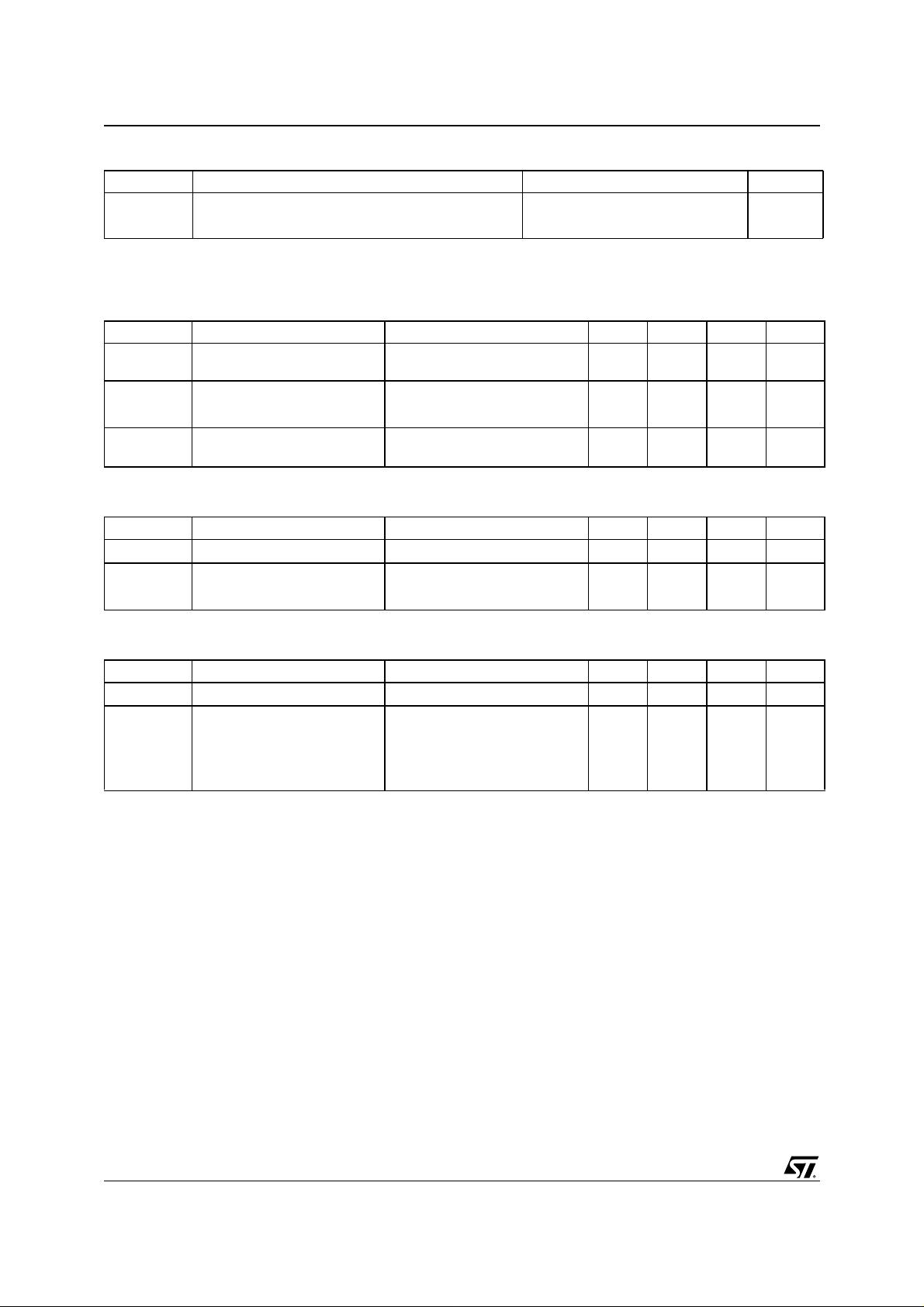
Safe Operating Area Thermal Impeda nce
3/9
Page 4
STB40NF10L
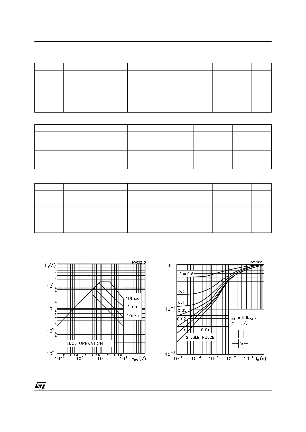
Output Characteristics
Transfer Characteristics
Static Drain-source On ResistanceTransco nductance
Gate Charge vs Gate-source Voltage
4/9
Capacitance Variations
Page 5
STB40NF10L
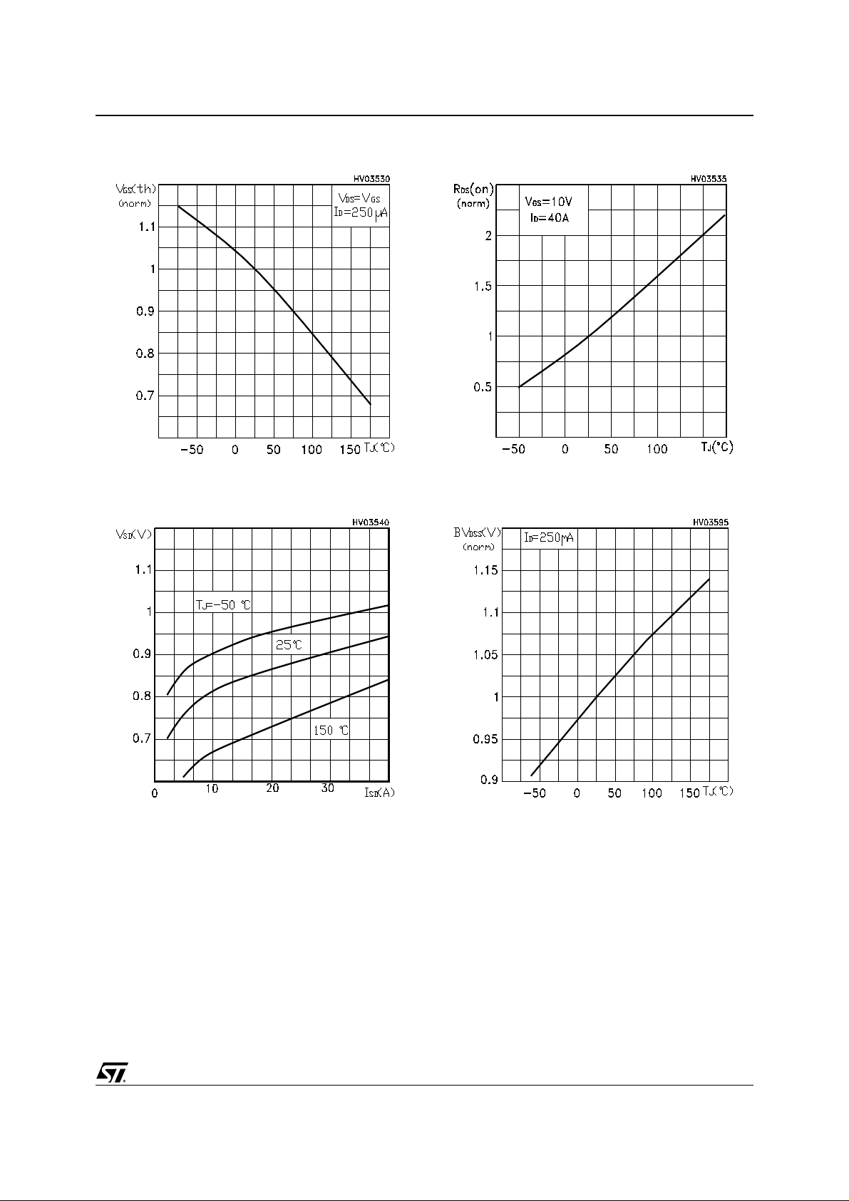
Normalized Gate Threshold Volta ge vs
Temperature
Source-drain Diode Forward Characteristics
Normalized On Resistance vs Temperature
Normalized Drain-Source Breakdown vs
Temperature
5/9
Page 6
STB40NF10L
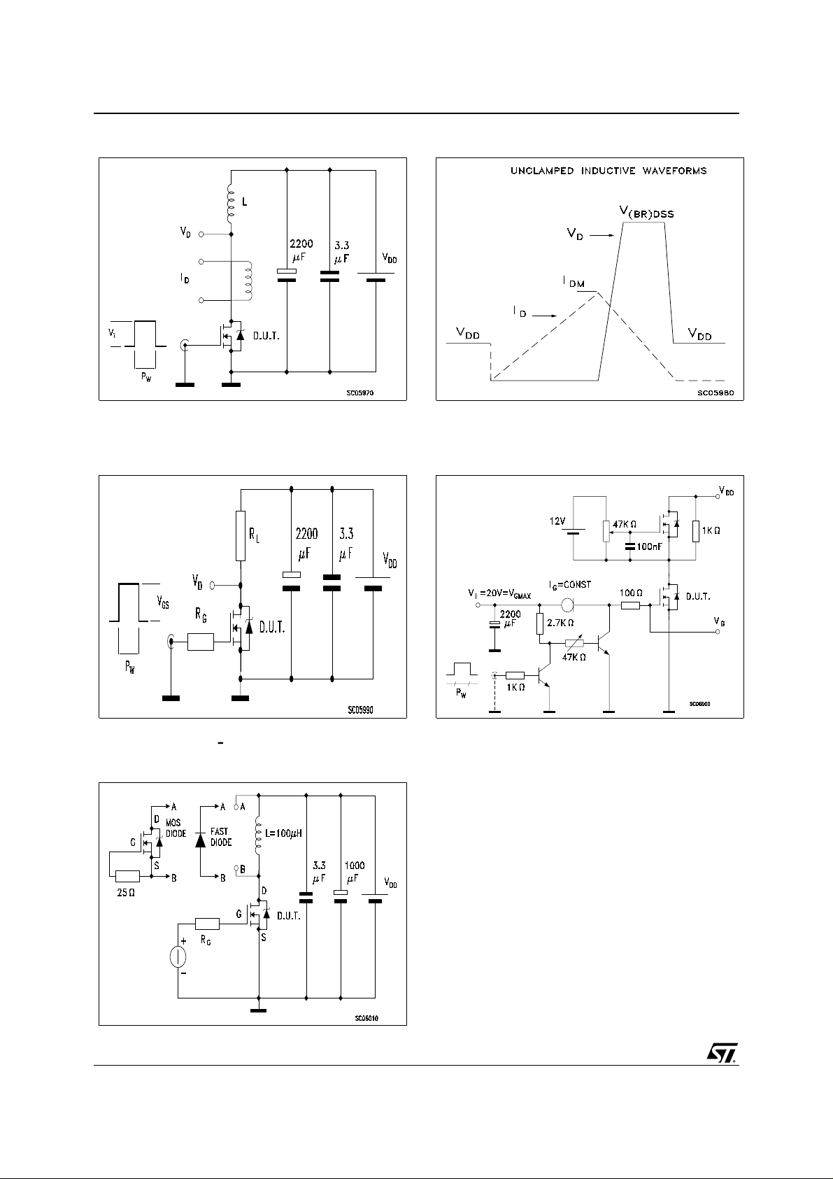
Fig. 2: Unclamped Inductive WaveformFig. 1: Unclamped Inductive Load Test Circuit
Fig. 3: Switching Times Test Circuit For
Resistive Load
Fig. 5: Test Circuit For Inductive Load Switching
And Diode Recovery Times
Fig. 4: Gate Charge test Circuit
6/9
Page 7

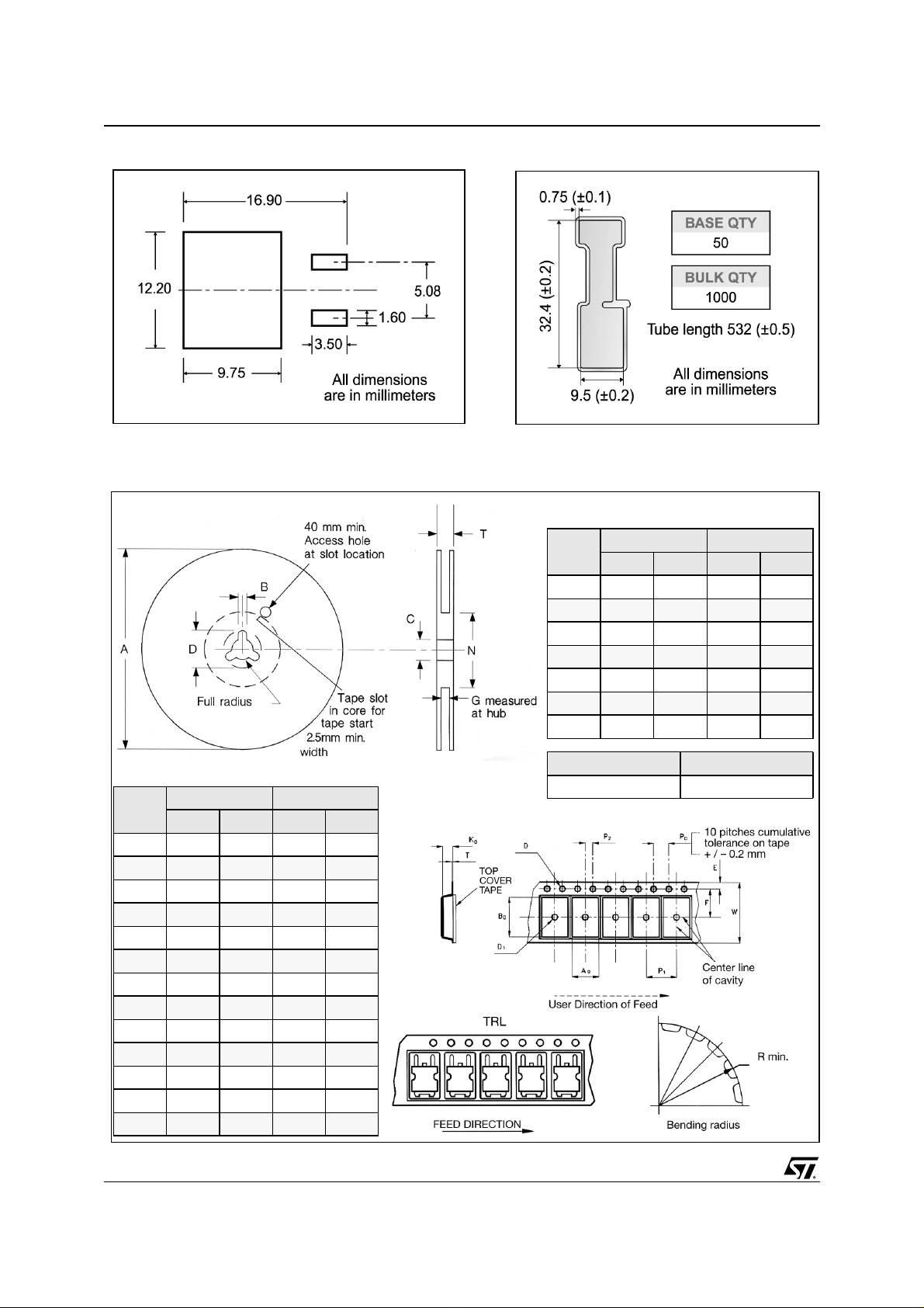
2
D
PAK MECH ANICAL DATA
STB40NF10L
DIM.
MIN. TYP MAX. MIN. TYP. MAX.
A 4.4 4.6 0.173 0.181
A1 2.49 2.69 0.098 0.106
A2 0.03 0.23 0.001 0.009
B 0.7 0.93 0.027 0.036
B2 1.14 1.7 0.044 0.067
C 0.45 0.6 0.017 0.023
C2 1.23 1.36 0.048 0.053
D 8.95 9.35 0.352 0.368
D1 8 0.315
E 10 10.4 0.393
E1 8.5 0.334
G 4.88 5.28 0.192 0.208
L 15 15.85 0.590 0.625
L2 1.27 1.4 0.050 0.055
L3 1.4 1.75 0.055 0.068
mm. inch
M 2.4 3.2 0.094 0.126
R 0.4 0.015
V2 0º8º
3
7/9
1
Page 8
STB40NF10L
D2PAK FOOTPRINT
TAPE AND REEL SHIPMENT (suffix ”T4”)*
TUBE SHIPMENT (no suffix)*
REEL MECHANICAL DATA
DIM.
A 330 12.992
B 1.5 0.059
C 12.8 13.2 0.504 0.520
D 20.2 0795
G 24.4 26.4 0.960 1.039
N 100 3.937
T 30.4 1.197
mm inch
MIN. MAX. MIN. MAX.
TAPE MECHANICAL DATA
DIM.
A0 10.5 10.7 0.413 0.421
B0 15.7 15. 9 0.618 0.626
D 1.5 1.6 0.059 0.063
D1 1.59 1.61 0.062 0.063
E 1.65 1.85 0.065 0.073
F 11.4 11.6 0.449 0.456
K0 4.8 5.0 0.189 0.197
P0 3.9 4.1 0.153 0.161
P1 11.9 12.1 0.468 0.476
P2 1.9 2.1 0.075 0.082
R50 1.574
T 0.25 0.35 0.0098 0.0137
W 23.7 24.3 0.933 0.956
* on sales type
8/9
mm inch
MIN. MAX. MIN. MAX.
BASE QTY BULK QTY
1000 1000
Page 9
STB40NF10L
Information furnished is believed to be accurate and reliable. However, STMicroelectronics assumes no responsibility for the consequences
of use of such informa tion n or for an y infring ement of patent s or other rig hts of third part ies which may resu lt from its use . No l i cen se i s
granted by implication or otherwise under any pa tent or patent rights of STM icroelectronics. Specification mentioned in this publication are
subject to change without notice. This publication supersedes and replaces all information previously supplied. STMicroelectronics products
are not authorized for use as critical compo nents in life support devices or systems without express written approval of STMicroelectronics.
Australia - Brazil - China - Finland - France - Germany - Hong Kong - India - Italy - Japan - Malaysia - Malta - Morocco -
The ST logo is a trademark of STMicroelectronics
© 2001 STMicroelectronics – Printed in Italy – All Rights Reserved
STMicroelectronics GROUP OF COMPANIES
Singapore - Spain - Sweden - Switzerland - United Kingdom - U.S.A.
http://www.st.com
9/9
 Loading...