

Page 1
STB40NF03L
N - CHANNEL 30V - 0.020 Ω - 40A D2PAK
STripFET POWER MOSFET
TYPE V
DSS
R
DS(o n)
I
D
ST B40NF03L 30 V < 0.022 Ω 40 A
■ TYPICALR
■ LOW THRESHOLDDRIVE
■ ADDSUFFIX ”T4” FORORDERING INTAPE
DS(on)
= 0.020 Ω
& REEL
DESCRIPTION
This PowerMOSFET is the latest developmentof
STMicroelectronics unique ”Single Feature
Size” strip-based process. The resulting
transistor shows extremely high packing density
for low on-resistance, rugged avalanche
characteristics and less critical alignment steps
therefore a remarkable manufacturing
reproducibility.
APPLICATIONS
■ HIGHCURRENT, HIGH SPEED SWITCHING
■ SOLENOIDAND RELAYDRIVERS
■ MOTORCONTROL, AUDIO AMPLIFIERS
■ DC-DC& DC-ACCONVERTERS
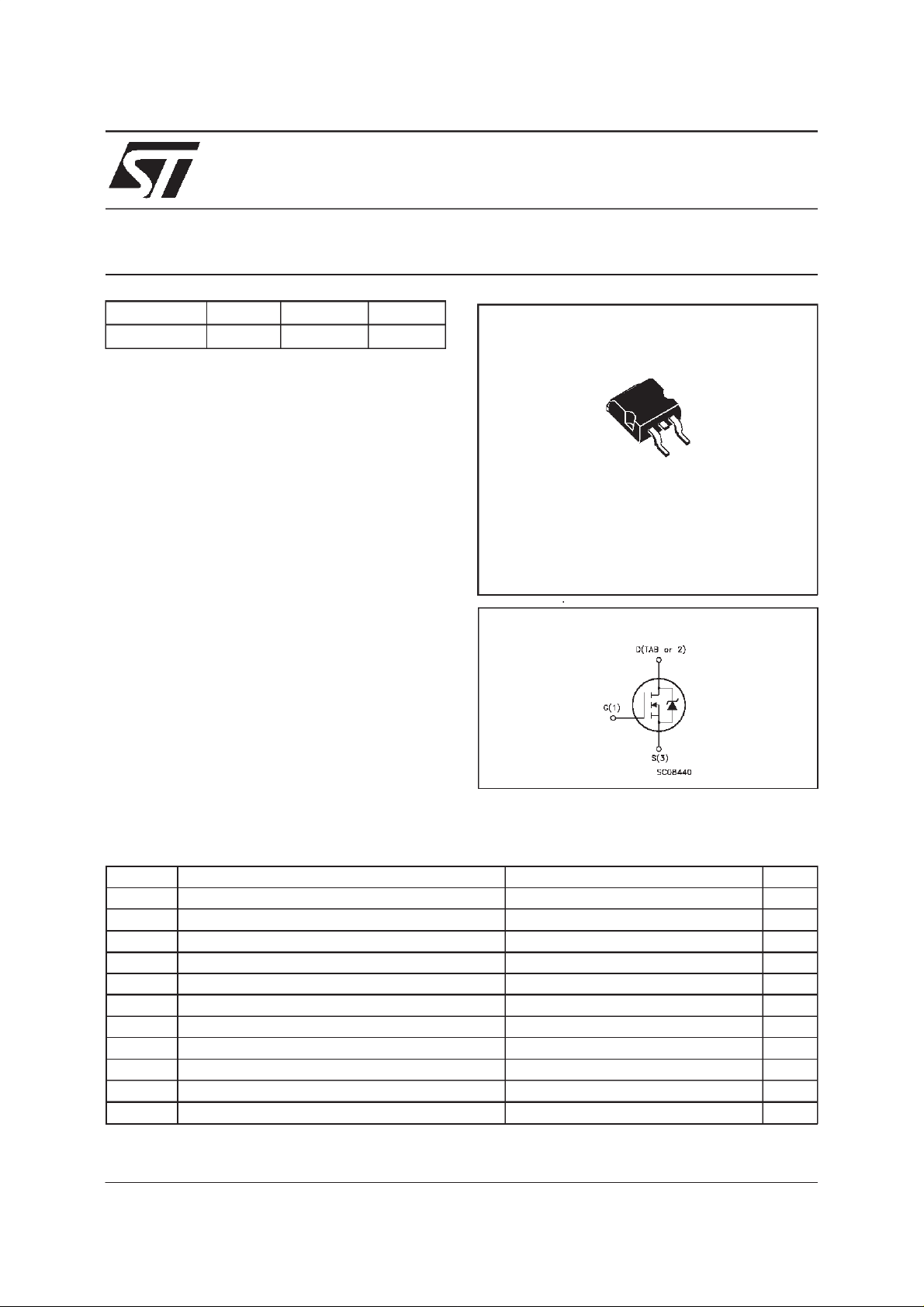
3
1
D2PAK
TO-263
(Suffix ”T4”)
INTERNAL SCHEMATIC DIAGRAM
ABSOLUTE MAXIMUM RATINGS
Symbol Parameter Value Uni t
V
V
V
I
DM
P
E
AS
T
(•) Pulse width limitedby safe operating area (1) starting Tj
October 1999
Dra in- sour c e Vol ta ge (VGS=0) 30 V
DS
Drain- gate Voltage (RGS=20kΩ)30V
DGR
Gate-s ource Volt age ± 20 V
GS
Dra in Current (conti nuous ) at Tc=25oC40A
I
D
Dra in Current (conti nuous ) at Tc= 100oC28A
I
D
(
Dra in Current (pulsed) 160 A
•)
Tot al Dissi pat io n at Tc=25oC70W
tot
Der ati ng Fact or 0.46 W/
(1) Single Pulse Avalanche Energy 250 m/ J
St orage Tem pe ra t ure -65 to 175
stg
Max. Operat ing Junction Tempe rat ur e 175
T
j
=25oC,ID=20A , VDD= 15V
o
C
o
C
o
C
1/8
Page 2
STB40NF03L
THERMAL DATA
R
thj-case
R
thj-amb
T
Ther mal Resistanc e Junct ion-case Max
Ther mal Resistanc e Junct ion-ambient Max
Maximum L ead Temperat ur e For Soldering Purpose
l
2.1
62.5
300
o
C/W
o
C/W
o
C
ELECTRICAL CHARACTERISTICS
=25oC unless otherwisespecified)
(T
case
OFF
Symbol Parameter Test Conditions Min. Typ. Max. Unit
V
(BR)DSS
Drain-source
ID=250µAVGS=0 30 V
Break dow n Voltage
I
DSS
I
GSS
Zero Gate Voltage
Drain Current (V
GS
Gat e- bod y Leakage
Current (V
DS
=0)
=0)
V
=MaxRating
DS
=MaxRating Tc=125oC
V
DS
V
= ± 20 V ± 100 nA
GS
1
10
ON(∗)
Symbol Parameter Test Conditions Min. Typ. Max. Unit
V
GS(th)
R
DS(on)
I
D(on)
Gate Threshold Voltage VDS=VGSID= 250 µ A11.72.5V
Sta t ic Drain-sour ce On
Resistance
On State Drain Current VDS>I
VGS=10V ID=20A
V
=4.5V ID=20A
GS
D(on)xRDS(on )max
0.018
0.028
0.022
0.035
40 A
VGS=10V
DYNAMIC
Symbol Parameter Test Conditions Min. Typ. Max. U nit
g
(∗)Forward
fs
Tr ansc on duc tance
C
C
C
Input Capacitance
iss
Out put Capacitance
oss
Reverse Transfer
rss
Capacit a nc e
VDS>I
D(on)xRDS(on )maxID
=20 A 20 S
VDS=25V f=1MHz VGS= 0 830
230
92
µA
µ
Ω
Ω
pF
pF
pF
A
2/8
Page 3
STB40NF03L
ELECTRICAL CHARACTERISTICS
(continued)
SWITCHINGON
Symbol Parameter Test Conditions Min. Typ. Max. U nit
t
d(on)
Tur n-on Delay T ime
Rise Time
t
r
VDD=15V ID=20A
R
=4.7
G
Ω
VGS=4.5V
35
205
(Resis t iv e Load, see fig. 3)
Q
Q
Q
Tot al Gate Charge
g
Gat e- Source Char g e
gs
Gate-Drain Charge
gd
VDD=24V ID=40A VGS=5V 18
7
8
23 nC
SWITCHINGOFF
Symbol Parameter Test Conditions Min. Typ. Max. U nit
t
d(off)
Tur n-of f Delay Time
t
Fall T ime
f
VDD=15V ID=20A
=4.7 Ω VGS=4.5V
R
G
90
240
(Resis t iv e Load, see fig. 3)
t
d(off)
Off-volt age Rise Tim e
t
Fall T ime
f
t
Cross-over Time
c
Vclamp = 24 V ID=20A
=4.7 Ω VGS=4.5V
R
G
(Indu ct iv e Load, see fig. 5)
150
155
340
SOURCEDRAIN DIODE
Symbol Parameter Test Conditions Min. Typ. Max. U nit
I
V
I
SDM
SD
Q
I
RRM
SD
t
Source-drain Current
(•)
Source-drain Current
40
160
(pulsed)
(∗)ForwardOnVoltage ISD=40A VGS=0 1.5 V
Reverse Recovery
rr
Time
Reverse Recovery
rr
ISD= 40 A di/dt = 100 A /µs
=15V Tj=150oC
V
DD
(see test circuit, fig. 5)
65
72
Charge
Reverse Recovery
2
Current
ns
ns
nC
nC
ns
ns
ns
ns
ns
A
A
ns
nC
A
(∗) Pulsed: Pulse duration = 300 µs, duty cycle 1.5%
(•) Pulse width limited by safeoperating area
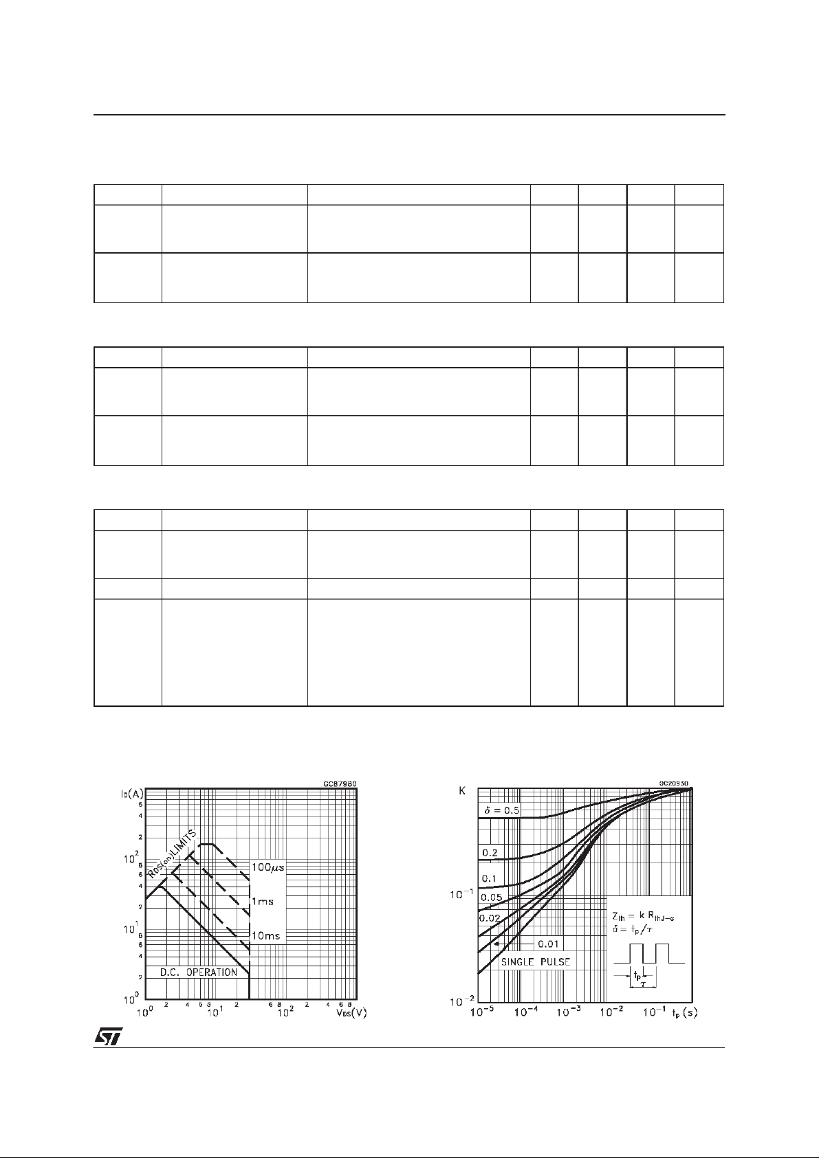
SafeOperating Area ThermalImpedance
3/8
Page 4

STB40NF03L
OutputCharacteristics
Transconductance
TransferCharacteristics
Static Drain-sourceOn Resistance
Gate Charge vs Gate-sourceVoltage
4/8
CapacitanceVariations
Page 5

STB40NF03L
NormalizedGate ThresholdVoltage vs
Temperature
Source-drainDiode Forward Characteristics
NormalizedOn Resistancevs Temperature
5/8
Page 6

STB40NF03L
Fig. 1: UnclampedInductiveLoad Test Circuit
Fig. 3: SwitchingTimesTest CircuitsFor
ResistiveLoad
Fig. 2:UnclampedInductive Waveform
Fig. 4: Gate Charge test Circuit
Fig. 5: TestCircuit ForInductiveLoad Switching
And Diode Recovery Times
6/8
Page 7

TO-263 (D2PAK) MECHANICAL DATA
STB40NF03L
DIM.
MIN. TYP. MAX. MIN. TYP. MAX.
A 4.4 4.6 0.173 0.181
A1 2.49 2.69 0.098 0.106
B 0.7 0.93 0.027 0.036
B2 1.14 1.7 0.044 0.067
C 0.45 0.6 0.017 0.023
C2 1.21 1.36 0.047 0.053
D 8.95 9.35 0.352 0.368
E 10 10.4 0.393 0.409
G 4.88 5.28 0.192 0.208
L 15 15.85 0.590 0.624
L2 1.27 1.4 0.050 0.055
L3 1.4 1.75 0.055 0.068
mm inch
D
A
C2
DETAIL”A”
C
A2
DETAIL”A”
A1
B2
E
L2
L
L3
B
G
P011P6/E
7/8
Page 8

STB40NF03L
Information furnished is believed tobeaccurateand reliable. However, STMicroelectronics assumesno responsibility for the consequences
of use of such information nor for any infringement of patents or other rights of third parties which may resultfrom its use. No license is
granted by implication or otherwise under any patent or patent rights of STMicroelectronics. Specificationmentioned in this publicationare
subjecttochange without notice.Thispublication supersedesand replacesall information previouslysupplied.STMicroelectronics products
are not authorizedfor useas critical components in lifesupport devices or systems without express written approval of STMicroelectronics.
The STlogo is a trademark of STMicroelectronics
1999STMicroelectronics – Printed in Italy – All Rights Reserved
STMicroelectronics GROUP OF COMPANIES
Australia - Brazil - China- Finland - France - Germany - Hong Kong - India - Italy - Japan - Malaysia - Malta - Morocco -
8/8
Singapore - Spain - Sweden - Switzerland - United Kingdom - U.S.A.
http://www.st.com
.
 Loading...