

Page 1
STB40NE03L-20
N - CHANNEL ENHANCEMENT MODE
” SINGLE FEATURE SIZE ” POWER MOSFET
TYPE V
■ TYPICALR
■ EXCEPTIONAL dv/dt CAPABILITY
■ LOW GATE CHARGE A 100
■ APPLICATIONORIENTED
DS(on)
DSS
= 0.014Ω
R
DS(on)
I
D
o
C
CHARACTERIZATION
■ FOR THROUGH-HOLE VERSIONCONTACT
SALESOFFICE
DESCRIPTION
This Power MOSFETis the latestdevelopment of
SGS-THOMSON unique ”Single Feature Size”
strip-based process. The resulting transistor
shows extremely high packing density for low onresistance, rugged avalanche characteristics and
less critical alignment steps therefore a remarkable manufacturingreproducibility.
APPLICATIONS
■ HIGH CURRENT, HIGHSPEEDSWITCHING
SOLENOIDAND RELAY DRIVERS
■ MOTORCONTROL, AUDIOAMPLIFIERS
■ DC-DC& DC-AC CONVERTERSIN HIGH
PERFORMANCEVRMs
■ AUTOMOTIVE ENVIRONMENT(INJECTION,
ABS, AIR-BAG, LAMPDRIVERS,Etc.)
ABSOLUTE MAXIMUM RATINGS
3
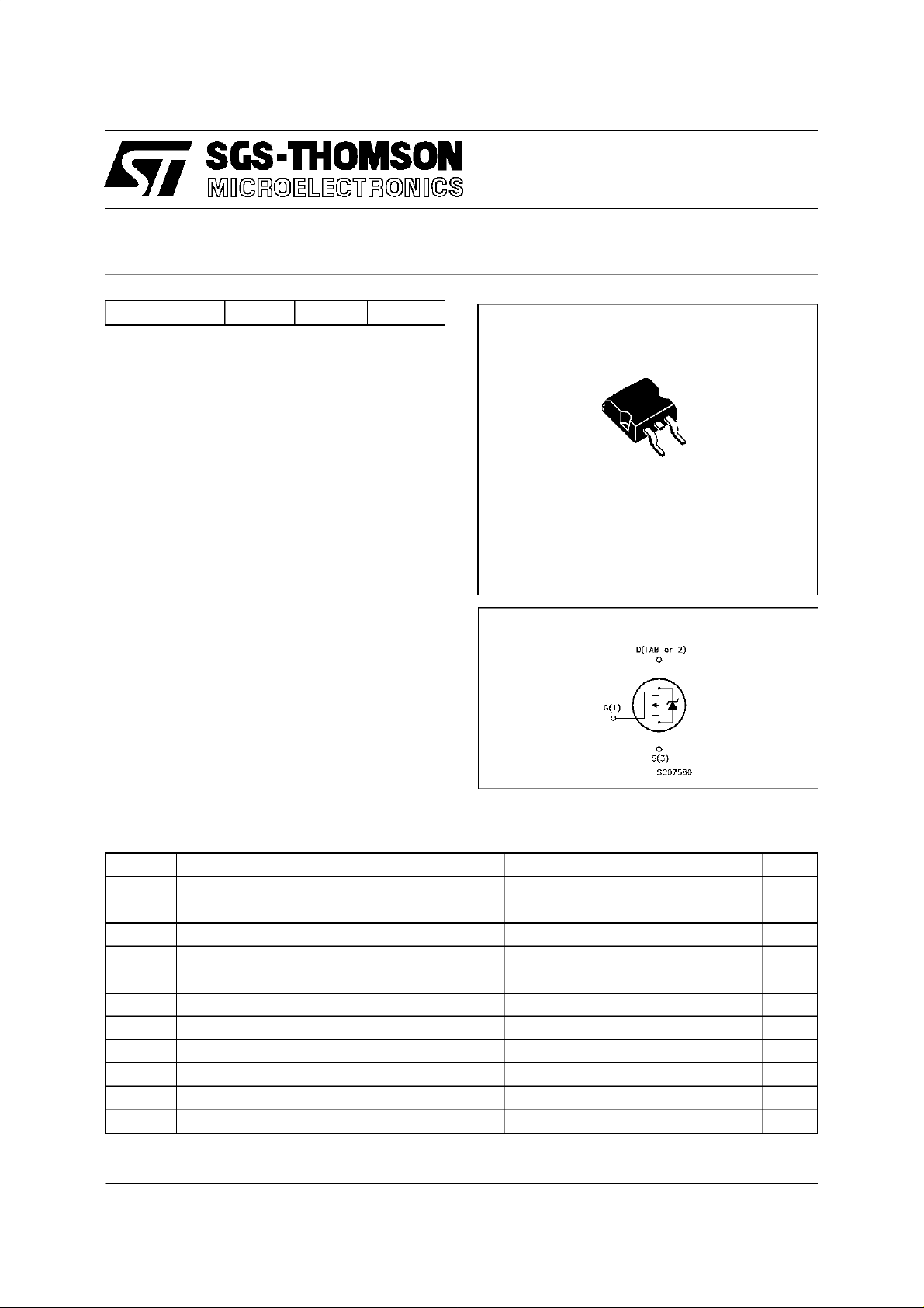
1
D2PAK
TO-263
(suffix ”T4”)
INTERNAL SCHEMATIC DIAGRAM
Symbol Parameter Value Unit
V
V
V
I
DM
P
Drain-sourc e Voltag e (VGS=0) 30 V
DS
Drain- gat e Voltag e (RGS=20kΩ)
DGR
Gate- source Voltage ± 15 V
GS
I
Drain Cur re n t (cont inuous) at Tc=25oC40A
D
I
Drain Cur re n t (cont inuous) at Tc=100oC28A
D
30 V
(•) Drain Current (pulsed) 160 A
Total Dissipation at Tc=25oC80W
tot
Derating Fa ctor 0.53 W/
dv/ dt(
1) Peak Diode Recov ery voltage slope 7 V/ns
T
(•) Pulsewidth limited bysafe operating area (1)ISD≤ 40 A,di/dt ≤ 300 A/µs, VDD≤ V
St orage Temper at ure -65 to 175
stg
T
Max. Operating Ju nction Temperature 175
j
(BR)DSS,Tj≤TJMAX
November 1997
o
C
o
C
o
C
1/8
Page 2
STB40NE03L-20
THERMAL DATA
R
thj-case
R
thj- amb
R
thc-sin k
T
AVALANCHE CHARACTERISTICS
Symbol Para met e r Max Valu e Uni t
I
AR
E
Ther mal Resist ance Junctio n- ca s e Max
Ther mal Resist ance Junctio n- ambient Max
Ther mal Resist ance Case-si nk Ty p
Maximum Lead T emperat ure For Soldering Purpos e
l
Avalanche Cur re nt , Rep et it i v e or Not-Re petitiv e
(pulse width limited by T
Single Pulse Avalanche Energy
AS
(starting T
=25oC, ID=IAR,VDD=15V)
j
max, δ <1%)
j
1.88
62.5
0.5
300
40 A
200 mJ
o
C/W
o
C/W
o
C/W
o
C
ELECTRICAL CHARACTERISTICS (T
=25oC unlessotherwise specified)
case
OFF
Symbol Parameter Test Cond itions Min. Typ. Max. Unit
V
(BR)DSS
Drain-sourc e
=250µAVGS=0
I
D
30 V
Breakdown V oltage
I
I
DSS
GSS
Zer o Gate V o lt age
Drain Cur re nt (V
GS
Gat e-body Leaka ge
Current (V
DS
=0)
=0)
=MaxRating
V
DS
V
=MaxRating Tc=125
DS
o
C
= ± 15 V
V
GS
1
10
± 100 nA
ON (∗)
Symbol Parameter Test Cond itions Min. Typ. Max. Unit
V
GS(th )
Gate Threshold
V
DS=VGSID
=250µA
11.82.5V
Voltage
R
DS(on)
I
D(on)
Stati c D rain-source On
Resistance
VGS=10V ID=20A
=5V ID=20A
V
GS
On State Drain Curre nt VDS>I
D(on)xRDS(on)max
0.014 0. 0 2
0.023ΩΩ
40 A
VGS=10V
DYNAMIC
Symbol Parameter Test Cond itions Min. Typ. Max. Unit
g
(∗)Forward
fs
Tr ansconduc tanc e
C
C
C
Input Capaci t ance
iss
Out put C apacit ance
oss
Reverse Transfer
rss
Capa cit an c e
VDS>I
D(on)xRDS(on)maxID
=20A 15 20 S
VDS=25V f=1MHz VGS= 0 1850
450
160
2400
590
210
µA
µA
pF
pF
pF
2/8
Page 3
STB40NE03L-20
ELECTRICAL CHARACTERISTICS (continued)
SWITCHINGON
Symbol Parameter Test Cond itions Min. Typ. Max. Unit
t
d(on)
Q
Q
Q
Turn-on Time
Rise Tim e
t
r
Total Gate Charge
g
Gat e-Sou rc e Charge
gs
Gate-Drain Charge
gd
VDD=15V ID=20A
=4.7 Ω VGS=5V
R
G
VDD=24V ID=40A VGS=5V 29
SWITCHINGOFF
Symbol Parameter Test Cond itions Min. Typ. Max. Unit
t
r(Voff)
t
Of f - voltag e Rise Time
t
Fall Time
f
Cross-ov er Time
c
VDD=24V ID=40A
=4.7 Ω VGS=5V
R
G
SOURCE DRAIN DIODE
Symbol Parameter Test Cond itions Min. Typ. Max. Unit
I
SD
I
SDM
V
SD
t
Q
I
RRM
(∗) Pulsed: Pulse duration =300 µs, duty cycle1.5 %
(•) Pulse width limited by safe operating area
Source-drain Current
(•)
Source-drain Current
(pulsed)
(∗) Forwar d On Vo lt age ISD=40A VGS=0 1.5 V
Reverse Recov ery
rr
Time
Reverse Recov ery
rr
= 40 A di/dt = 100 A /µs
I
SD
=20V Tj=150oC
V
DD
Charge
Reverse Recov ery
Current
25
16033210
38 nC
12
14
25
120
155
33
160
210
40
160
50
0.9
3.5
ns
ns
nC
nC
ns
ns
ns
A
A
ns
µC
A
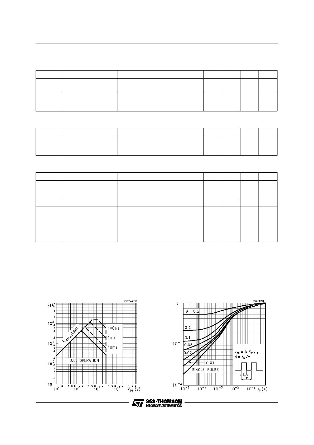
Safe Operating Area ThermalImpedance
3/8
Page 4

STB40NE03L-20
OutputCharacteristics
Transconductance
TransferCharacteristics
StaticDrain-sourceOn Resistance
GateCharge vs Gate-sourceVoltage
4/8
CapacitanceVariations
Page 5

STB40NE03L-20
Normalized Gate Threshold Voltage vs
Temperature
Source-drainDiode Forward Characteristics
Normalized On Resistance vs Temperature
5/8
Page 6

STB40NE03L-20
Fig. 1: Unclamped Inductive Load TestCircuit
Fig. 3: SwitchingTimes Test CircuitsFor
ResistiveLoad
Fig. 2: Unclamped Inductive Waveform
Fig. 4: Gate Charge test Circuit
Fig. 5: Test Circuit For InductiveLoad Switching
And Diode RecoveryTimes
6/8
Page 7

TO-263 (D2PAK) MECHANICAL DATA
STB40NE03L-20
DIM.
MIN. TYP. MAX. MIN. TYP. MAX.
A 4.3 4.6 0.169 0.181
A1 2.49 2.69 0.098 0.106
B 0.7 0.93 0.027 0.036
B2 1.25 1.4 0.049 0.055
C 0.45 0.6 0.017 0.023
C2 1.21 1.36 0.047 0.053
D 8.95 9.35 0.352 0.368
E 10 10.28 0.393 0.404
G 4.88 5.28 0.192 0.208
L 15 15.85 0.590 0.624
L2 1.27 1.4 0.050 0.055
L3 1.4 1.75 0.055 0.068
mm inch
E
A
C2
L2
D
L
L3
B2
B
A1
C
G
P011P6/C
7/8
Page 8

STB40NE03L-20
Information furnished is believedtobe accurate and reliable. However,SGS-THOMSON Microelectronics assumesno responsability for the
consequencesof use ofsuch informationnor for any infringement of patents or otherrights of third parties which may resultsfromits use. No
licenseisgranted by implicationor otherwise underany patentor patent rights of SGS-THOMSON Microelectronics. Specificationsmentioned
in this publicationare subjectto change without notice.This publicationsupersedes and replaces all information previously supplied.
SGS-THOMSONMicroelectronics productsarenotauthorized for useascritical components in life supportdevicesor systems withoutexpress
writtenapproval of SGS-THOMSON Microelectonics.
1997 SGS-THOMSONMicroelectronics- Printedin Italy - AllRights Reserved
Australia- Brazil - Canada- China - France - Germany- Italy - Japan - Korea - Malaysia- Malta- Morocco- The Netherlands-
Singapore- Spain- Sweden- Switzerland -Taiwan- Thailand - United Kingdom - U.S.A
SGS-THOMSONMicroelectronics GROUPOF COMPANIES
...
8/8
 Loading...