

Page 1
STB3NC60
N - CHANNEL600V - 3.3Ω -3A-D2PAK/I2PAK
TYPE V
DSS
R
DS(on)
I
D
ST B3 NC60 600 V < 3 .6 Ω 3A
ν TYPICALR
ν EXTREMELY HIGHdv/dt CAPABILITY
ν 100% AVALANCHETESTED
ν VERY LOW INTRINSIC CAPACITANCES
ν GATECHARGE MINIMIZED
DS(on)
= 3.3 Ω
DESCRIPTION
The PowerMESHII is the evolution of the first
generation of MESH OVERLAY. The layout
refinements introduced greatly improve the
Ron*area figure of merit while keeping the device
at the leading edge for what concerns switching
speed, gatecharge and ruggedness.
APPLICATIONS
ν HIGH CURRENT, HIGH SPEEDSWITCHING
ν SWITCHMODEPOWER SUPPLIES (SMPS)
ν DC-ACCONVERTERSFOR WELDING
EQUIPMENTAND UNINTERRUPTIBLE
POWERSUPPLIESAND MOTORDRIVE
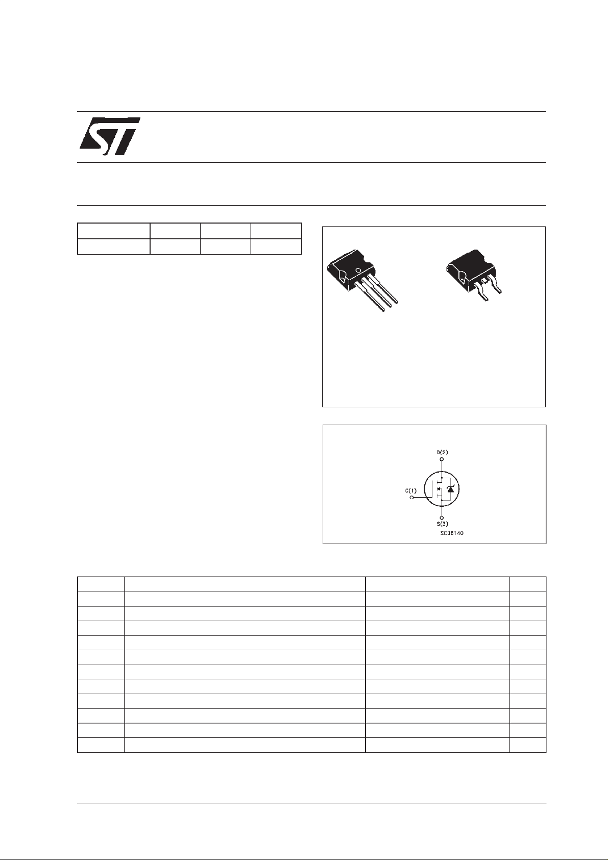
PowerMESH
3
2
1
I2PAK
TO-262
(Suffix”-1”)
ΙΙ MOSFET
D2PAK
TO-263
(Suffix ”T4”)
INTERNAL SCHEMATIC DIAGRAM
3
1
ABSOLUTE MAXIMUM RATINGS
Symbol Parameter Value Uni t
V
V
V
I
DM
P
dv/dt(
T
(•) Pulse width limited by safe operating area (1)ISD≤3A, di/dt ≤ 100 A/µs, VDD≤ V
February 2000
Drain-source Volt age (VGS= 0 ) 600 V
DS
Drain- gate Voltage ( RGS=20kΩ)
DGR
Gate-s ource Voltage ± 30 V
GS
Drain Current (c ont in uous ) at Tc=25oC3A
I
D
I
Drain Current (c ont in uous ) at Tc= 100oC 1.9 A
D
600 V
(•) Drain Current (p ulsed) 12 A
Tot al D issipation at Tc=25oC80W
tot
Derating Factor 0.64 W/
1) Peak Diode Rec overy voltage slope 4 V/ns
St orage T e m perature -65 to 150
stg
Max. O per ating J u nc tion Temperature 150
T
j
,Tj≤T
(BR)DSS
JMAX
o
C
o
C
o
C
1/9
Page 2
STB3NC60
THERMAL DATA
R
thj-cas e
R
thj-amb
R
thc-sin k
T
AVALANCHE CHARACTERISTICS
Symb ol Parameter Max Value Uni t
I
AR
E
Therma l Resist ance Junct i on- case Max 1.56
Therma l Resist ance Junct i on- ambient Max
Therma l Resist ance Case-sink Typ
Maxim um Lead Tem pe ra t ure For Soldering P urpose
l
Avalanc h e Current , Repe t it ive or N ot-Repetitive
(pulse w idth limited b y T
Single P ulse A v alanche Energy
AS
(starting T
=25oC, ID=IAR,VDD=50V)
j
max)
j
62.5
0.5
300
3A
100 mJ
o
C/W
o
C/W
o
C/W
o
C
ELECTRICAL CHARACTERISTICS (T
=25oC unlessotherwisespecified)
case
OFF
Symb ol Parameter Test C o n ditions Mi n . Typ . Max. Unit
V
(BR) DSS
Drain-s ource
= 250 µAVGS=0
I
D
600 V
Break down Volt age
I
DSS
I
GSS
Zero Gate Voltage
Drain Cur rent (V
GS
Gate-body Leaka ge
Current (V
DS
=0)
=0)
V
=MaxRating
DS
= Max Rating Tc= 125oC
V
DS
= ± 30 V
V
GS
1
50
± 100 nA
ON (∗)
Symb ol Parameter Test C o n ditions Mi n . Typ . Max. Unit
V
GS(th)
R
DS(on)
Gate Th re sho ld Volt age
Static D rain-sourc e O n
V
DS=VGSID
=250µA
VGS= 10V ID= 1.5 A 3.3 3.6 Ω
234V
Resistance
I
D(on)
On State Drain Current VDS>I
D(on)xRDS(on)max
3A
VGS=10V
DYNAMIC
Symb ol Parameter Test C o n ditions Mi n . Typ . Max. Unit
g
(∗)Forward
fs
Transconduct ance
C
C
C
Input Capac itance
iss
Output Capacitance
oss
Reverse Transfer
rss
Capacit ance
VDS>I
D(on)xRDS(on)maxID
=1.5A 2 S
VDS=25V f=1MHz VGS= 0 400
57
7
µA
µA
pF
pF
pF
2/9
Page 3
STB3NC60
ELECTRICAL CHARACTERISTICS (continued)
SWITCHING ON
Symb ol Parameter Test C o n ditions Mi n . Typ . Max. Unit
t
d(on)
t
r
Turn-on Time
Rise Time
VDD=300V ID=1.5A
=4.7 Ω VGS=10V
R
G
(see test circuit, figure 3)
Q
Q
Q
Total Gate Charge
g
Gate-Sourc e Char ge
gs
Gate-Drain Char g e
gd
VDD=480V ID=3A VGS=10V 13
SWITCHING OFF
Symb ol Parameter Test C o n ditions Mi n . Typ . Max. Unit
t
r(Voff)
t
Off -volt age Ris e Time
Fall Time
t
f
Cross -over Time
c
VDD=480V ID=3A
=4.7 Ω VGS=10V
R
G
(see test circuit, figure 5)
SOURCEDRAINDIODE
Symb ol Parameter Test C o n ditions Mi n . Typ . Max. Unit
I
SD
I
SDM
V
SD
t
Q
I
RRM
(∗) Pulsed: Pulse duration = 300µs, dutycycle 1.5 %
(•) Pulse width limited by safe operatingarea
Source-drain Current
(•)
Source-drain Current
(pulsed)
(∗)ForwardOnVoltage ISD=3A VGS=0 1.6 V
Revers e R ec overy
rr
Time
Revers e R ec overy
rr
= 3 A di/dt = 100 A/µs
I
SD
=100V Tj= 150oC
V
DD
(see test circuit, figure 5)
Charge
Revers e R ec overy
Current
9
13
18.2 nC
2.3
4.4
13
15
21
3
12
420
1.5
7.1
ns
ns
nC
nC
ns
ns
ns
A
A
ns
µC
A
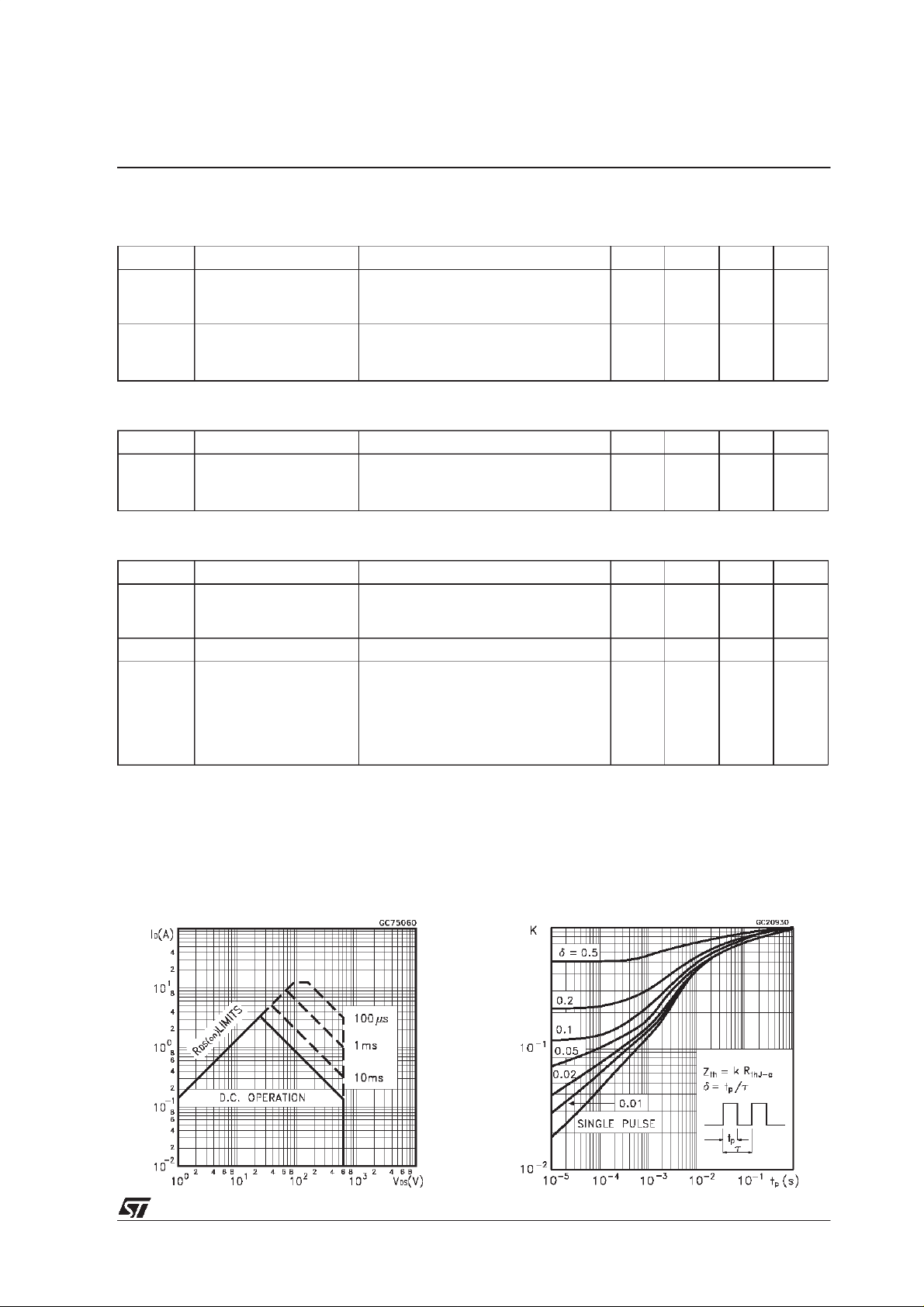
Safe Operating Area for D2PAK/I2PAK ThermalImpedanceforD2PAK/I2PAK
3/9
Page 4

STB3NC60
OutputCharacteristics
Transconductance
TransferCharacteristics
StaticDrain-source On Resistance
Gate Chargevs Gate-sourceVoltage
4/9
CapacitanceVariations
Page 5

STB3NC60
NormalizedGate Threshold Voltage vs
Temperature
Source-drainDiode ForwardCharacteristics
Normalized On Resistance vs Temperature
5/9
Page 6

STB3NC60
Fig. 1: UnclampedInductive Load Test Circuit
Fig. 3: Switching Times Test Circuits For
ResistiveLoad
Fig. 2: UnclampedInductiveWaveform
Fig. 4: GateChargetest Circuit
Fig. 5: TestCircuitFor InductiveLoad Switching
And DiodeRecovery Times
6/9
Page 7

TO-262 (I2PAK) MECHANICAL DATA
STB3NC60
DIM.
MIN. TYP. MAX. MIN. TYP. MAX.
A 4.3 4.6 0.169 0.1 81
A1 2.49 2.69 0.098 0.106
B 0.7 0.93 0.027 0.036
B1 1.2 1.38 0.047 0.054
B2 1.25 1.4 0.049 0.055
C 0.45 0.6 0.017 0.023
C2 1.21 1.36 0.047 0.053
D 8.95 9.35 0.352 0.368
e 2.44 2.64 0.096 0.104
E 10 10.28 0.393 0.404
L 13.2 13.5 0. 519 0.5 31
L1 3.48 3.78 0.137 0.149
L2 1.27 1.4 0.050 0.055
mm inch
CA1
A
C2
B2
B
e
E
L1
L2
D
L
P011P5/C
7/9
Page 8

STB3NC60
TO-263 (D2PAK) MECHANICAL DATA
DIM.
MIN. TYP. MAX. MIN. TYP. MAX.
A 4 .3 4.6 0.169 0.181
A1 2.49 2.69 0.098 0.106
B 0.7 0.93 0.027 0.036
B2 1.25 1.4 0.049 0.055
C 0.45 0.6 0.017 0.023
C2 1.21 1.36 0.047 0.053
D 8.95 9.35 0.352 0.368
E 10 10.28 0.393 0.404
G 4.88 5.28 0.192 0.208
L 15 15.85 0.590 0.624
L2 1.27 1.4 0.050 0.055
L3 1.4 1.75 0.055 0.068
mm inch
E
A
C2
L2
D
L
L3
B2
B
A1
C
G
P011P6/C
8/9
Page 9

STB3NC60
Information furnished is believed to be accurate and reliable. However, STMicroelectronics assumes no responsibilityfor the consequences
of use of such information nor for any infringement of patents or other rights of third parties which may result from its use. No license is
granted by implication or otherwise under any patent or patentrights of STMicroelectronics. Specification mentioned in this publication are
subject to change without notice.This publication supersedesand replaces allinformation previously supplied.STMicroelectronicsproducts
are not authorized foruse as critical components in life support devicesor systems without expresswritten approval of STMicroelectronics.
The ST logo is a trademark of STMicroelectronics
1999 STMicroelectronics – Printed in Italy – All Rights Reserved
STMicroelectronics GROUP OF COMPANIES
Australia - Brazil - China - Finland - France- Germany - Hong Kong- India - Italy - Japan - Malaysia - Malta - Morocco -
Singapore - Spain - Sweden -Switzerland - United Kingdom - U.S.A.
http://www.st.com
.
9/9
 Loading...