

Page 1
STP35NF10
STB35NF10
N-CHANNEL 100V - 0.030Ω -40ATO-220/D2PAK
LOW GATE CHARGE STripFET™ POWER MOSFET
TYPE V
STP35NF10
STB35NF10
■ TYPICAL R
■ EXCEPTIONAL dv/dt CAPABILITY
■ 100% AVALANCHE TESTED
■ APPLICATION ORIENTED
DS
DSS
100 V
100 V
(on) = 0.030Ω
R
DS(on)
< 0.035 Ω
< 0.035 Ω
I
D
40 A
40 A
CHARACTERIZATION
DESCRIPTION
This Power Mosfet series realized with STMicroelectronics uniqueSTripFET process hasspecifical ly been designed to minimize input capacitance and
gate charge. It is therefore suitable as primary
switch in advanced high-efficiency isolated DC-DC
converters for Telecom and Computer application. It
is also intended for any application with low gate
charge drive requirements.
APPLICATIONS
■ HIGH-EFFICIENCY DC-DC CONVERTERS
■ UPS AND MOTOR CONTRO L
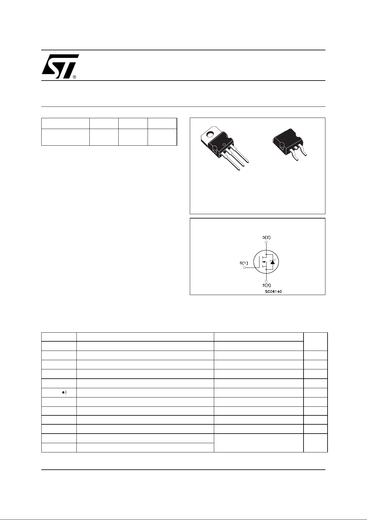
3
1
D2PAK
TO-220
3
2
1
INTERNAL SCHEMATIC DIAGRAM
ABSOLUTE MAXIMUM RATINGS
Symbol Parameter Value Unit
V
DS
V
DGR
V
GS
I
D
I
D
I
DM
P
TOT
dv/dt (1) Peak Diode Recovery voltage slope 13 V/ns
E
AS
T
stg
T
j
(●) Pulse width limited by safe operating area
Drain-source Voltage (VGS=0)
Drain-gate Voltage (RGS=20kΩ)
100 V
100 V
Gate- source Voltage ±20 V
Drain Current (continuous) at TC= 25°C
Drain Current (continuous) at TC= 100°C
()
Drain Current (pulsed) 160 A
Total Dissipation at TC= 25°C
40 A
28 A
115 W
Derating Factor 0.77 W/°C
(2)
Single Pulse Avalanche Energy 300 mJ
Storage Temperature
Operating Junction Temperature
(1) ISD≤35A, di/dt ≤300A/µs, VDD≤ V
(2) Starting Tj= 25°C, ID= 20A, VDD=80V
–55to175 °C
(BR)DSS,Tj≤TJMAX.
1/10April 2003
Page 2
STP35NF10 - STB35NF1 0
THERMAL DATA
Rthj-case Thermal Resistance Junction-case Max 1.30 °C/W
Rthj-amb Thermal Resistance Junction-ambient Max 62.5 °C/W
T
l
ELECTRICAL CHARACTERISTICS (TCASE = 25 °C UNLESS OTHERWISE SPECIFIED)
OFF
Symbol Parameter Test Conditions Min. Typ. Max. Unit
V
(BR)DSS
I
DSS
I
GSS
ON (1)
Symbol Parameter Test Conditions Min. Typ. Max. Unit
V
GS(th)
R
DS(on)
Maximum Lead Temperature For Soldering Purpose 300 °C
Drain-source
ID= 250 µA, VGS= 0 100 V
Breakdown Voltage
Zero Gate Voltage
Drain Current (V
GS
=0)
Gate-body Leakage
Current (V
DS
=0)
Gate Threshold Voltage
Static Drain-source On
V
= Max Rating
DS
VDS= Max Rating, TC= 125 °C
V
= ±20V ±100 nA
GS
V
DS=VGS,ID
VGS=10V,ID= 17.5 A
= 250µA
234V
0.030 0.035 Ω
1µA
10 µA
Resistance
DYNAMIC
Symbol Parameter Test Conditions Min. Typ. Max. Unit
(1) Forward Transconductance VDS=15V,ID=17.5A 20 S
g
fs
C
iss
C
oss
C
rss
Input Capacitance
Output Capacitance 220 pF
Reverse Transfer
Capacitance
V
=25V,f=1MHz,VGS=0
DS
1550 pF
95 pF
2/10
Page 3
STP35NF10
ELECTRICAL CHARACTERISTICS (CONTINUED)
SWITCHING ON
Symbol Parameter Test Conditions Min. Typ. Max. Unit
V
t
d(on)
Q
Q
Q
t
r
g
gs
gd
Turn-on Delay Time
Rise Time 60 ns
Total Gate Charge VDD=80V,ID=35A,VGS= 10V 55 nC
Gate-Source Charge 12 nC
Gate-Drain Charge 20 nC
SWITCHING OFF
Symbol Parameter Test Conditions Min. Typ. Max. Unit
t
d(off)
t
f
Turn-off-Delay Time
Fall Time
SOURCE DRAIN DIODE
Symbol Parameter Test Conditions Min. Typ. Max. Unit
I
SD
I
SDM
V
SD
t
rr
Q
rr
I
RRM
Note: 1. Pulsed: Pulse duration = 300 µs, duty cycle 1.5 %.
2. Pulse width limited by safe operating area.
Source-drain Current 40 A
(2)
Source-drain Current (pulsed) 160 A
(1)
Forward On Voltage
Reverse Recovery Time
Reverse Recovery Charge
Reverse Recovery Current
=50V,ID= 17.5 A
DD
= 4.7Ω VGS=10V
R
G
(see test circuit, Figure 3)
VDD= 50V, ID=17.5A,
R
=4.7Ω, VGS= 10V
G
(see test circuit, Figure 3)
ISD=35A,VGS=0
= 35 A, di/dt = 100A/µs,
I
SD
V
=25V,Tj= 150°C
DD
(see test circuit, Figure 5)
17 ns
60
15
1.5 V
160
720
9
ns
ns
ns
nC
A
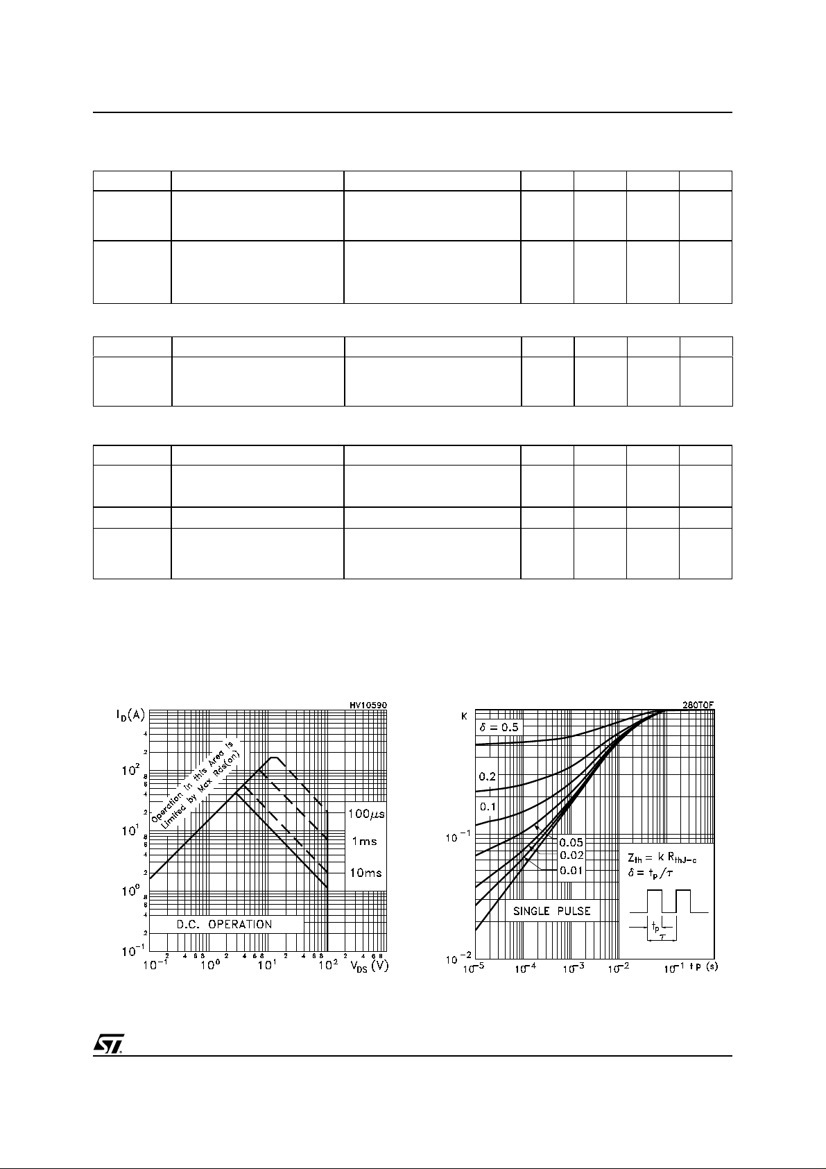
Thermal ImpedenceSafe Operating Area
3/10
Page 4

STP35NF10 - STB35NF1 0
Output Characteristics Transfer Characteristics
Transconductance Static Drain-source On Resistance
4/10
Capacitance VariationsGate Charge vs Gate-source Voltage
Page 5

STP35NF10
Normalized Gate Thereshold Voltage vs Temp. Normalized On Resistance vs Temperature
Source-drain Diode Forward Characteristics
5/10
Page 6

STP35NF10 - STB35NF1 0
Fig. 2: Unclamped In duc tive WaveformFig. 1: Unclamped Inductive Load Test Circuit
Fig. 3: Switching Times Tes t Circuit For
Resistive Load
Fig. 5: Test Circuit For Inductive Load Switching
And Diode Recovery Times
Fig. 4: Gate Charge test Circuit
6/10
Page 7

TO-220 MECHANICAL DATA
STP35NF10
DIM.
A 4.40 4.60 0.173 0.181
b 0.61 0.88 0.024 0.034
b1 1.15 1.70 0.045 0.066
c 0.49 0.70 0.019 0.027
D 15.25 15.75 0.60 0.620
E 10 10.40 0.393 0.409
e 2.40 2.70 0.094 0.106
e1 4.95 5.15 0.194 0.202
F 1.23 1.32 0.048 0.052
H1 6.20 6.60 0.244 0.256
J1 2.40 2.72 0.094 0.107
L 13 14 0.511 0.551
L1 3.50 3.93 0.137 0.154
L20 16.40 0.645
L30 28.90 1.137
øP 3.75 3.85 0.147 0.151
Q 2.65 2.95 0.104 0.116
MIN. TYP MAX. MIN. TYP. MAX.
mm. inch
7/10
Page 8

STP35NF10 - STB35NF1 0
D2PAK MECHANICAL DATA
DIM.
MIN. TYP MAX. MIN. TYP. MAX.
A 4.4 4.6 0.173 0.181
A1 2.49 2.69 0.098 0.106
A2 0.03 0.23 0.001 0.009
B 0.7 0.93 0.027 0.036
B2 1.14 1.7 0.044 0.067
C 0.45 0.6 0.017 0.023
C2 1.23 1.36 0.048 0.053
D 8.95 9.35 0.352 0.368
D1 8 0.315
E 10 10.4 0.393
E1 8.5 0.334
G 4.88 5.28 0.192 0.208
L 15 15.85 0.590 0.625
L2 1.27 1.4 0.050 0.055
L3 1.4 1.75 0.055 0.068
mm. inch
M 2.4 3.2 0.094 0.126
R 0.4 0.015
V2 0º 8º
3
8/10
1
Page 9

D2PAK FOOTPRINT
TAPE AND REEL SHIPMENT (suffix ”T4”)*
STP35NF10
TUBE SHIPMENT (no suffix)*
REEL MECHANICAL DATA
TAPE MECHANICAL DATA
DIM.
A0 10.5 10.7 0.413 0.421
B0 15.7 15.9 0. 618 0.626
D 1.5 1.6 0.059 0.063
D1 1.59 1.61 0.062 0.063
E 1.65 1.85 0.065 0.073
F 11.4 11.6 0.449 0.456
K0 4.8 5.0 0. 189 0.197
P0 3.9 4.1 0.153 0.161
P1 11.9 12.1 0.468 0.476
P2 1.9 2.1 0.075 0.082
R 50 1.574
T 0.25 0.35 0.0098 0.0137
W 23.7 24.3 0.933 0.956
mm inch
MIN. MAX. MIN. MAX.
DIM.
A 330 12.992
B 1.5 0.059
C 12.8 13.2 0.504 0.520
D 20.2 0795
G 24.4 26.4 0.960 1.039
N 100 3.937
T 30.4 1.197
BASE QTY BULK QTY
mm inch
MIN. MAX. MIN. MAX.
1000 1000
* on sales ty pe
9/10
Page 10

STP35NF10 - STB35NF1 0
Information furnished is believed to be accurate and reliable. However, STMicroelectronics assumes no responsibility for the
consequences of u se of such inform ation nor for any in fring ement of p atents or o ther ri ghts of th ird p arties which may r esul t f rom
its use. No license is granted by implication or otherwise under any patent or patent rights of STMicroelectronics. Specifications
mentioned in this publication are subject to change without notice. This publication supersedes and replaces all information
previously supplied. STMicroelectronics products are not authorized for use as critical components in life support devices or
systems without express written approval of STMicroelectronics.
Australia - Brazil - Canada - China - Finland - France - Germany - Hong Kong - India - Israel - Italy - Japan - Malaysia - Malta - Morocco
© The ST logo is a registered trademark of STMicroelectronics
© 2003 STMicroelectronics - Printed in Italy - All Rights Reserved
Singapore - Spain - Sweden - Switzerland - United Kingdom - United States.
STMicroelectronics GROUP OF COMPANIES
© http://www.st.com
10/10
 Loading...