

Page 1
STB30N10
N - CHANNEL 100V - 0.06Ω - 30A - D2PAK
POWER MOS TRANSISTOR
TYPE V
DSS
R
DS(on)
I
D
STB30N10 100 V < 0.07 Ω 30 A
■
TYPICAL R
■
AVALANCHE RUGG ED TECHNOLO GY
■
100% AVALANCHE TESTED
■
REPETITIVE AVALANCHE DATA AT 100oC
■
LOW GATE CHARGE
■
VERY HIGH CURRENT CAPABILITY
■
APPLICATION ORIENTED
DS(on)
= 0.06
Ω
CHARACTERIZATION
■
SURFACE-MO UNTING D2P AK (TO-263)
POWER PACKAGE IN TUBE (NO SUF F IX )
OR IN TAPE & REEL (SUFFIX "T4")
APPLICATIONS
■
HIGH CURRENT, HIGH SPEED SWITCH ING
■
SOLENOID AND RELAY DRIVERS
■
REGULATORS
■
DC-DC & DC-AC CONVERTERS
■
MOTOR CONTROL, AUDIO AMPLIFIERS
■
AUTOMOTIVE ENVIRONMENT (INJECTION,
ABS, AIR-BAG, LAMPDRIVERS, Etc.)
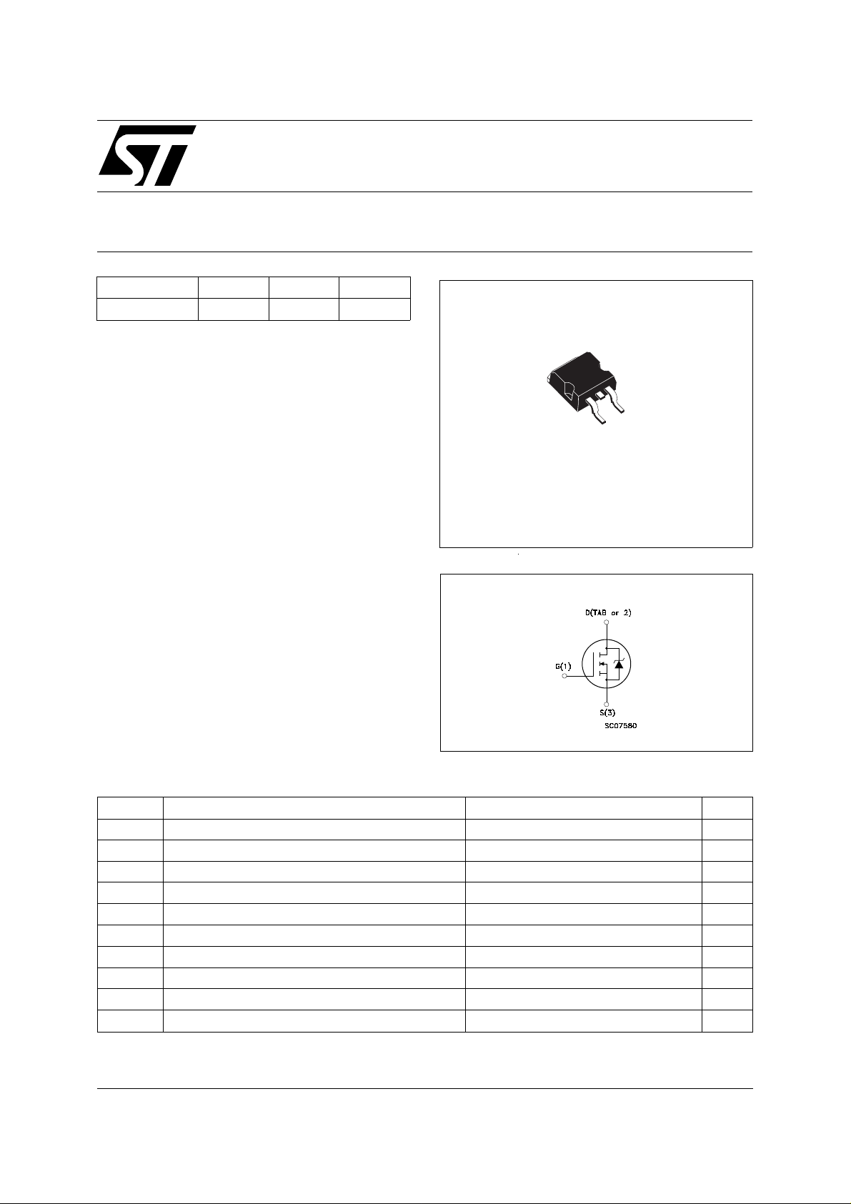
3
1
D2PAK
TO-263
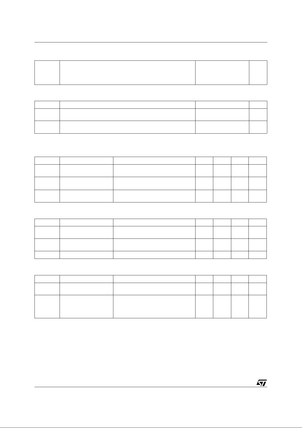
INTERNAL SCHEMATIC DIAGRAM
ABSOLUTE MAXIMUM RATINGS
Symbol Parameter Value Unit
V
V
V
I
DM
P
T
(•) Pulse width limited by safe operating area
September 1998
Drain-source Voltage (VGS = 0) 100 V
DS
Drain- gate Voltage (RGS = 20 kΩ)
DGR
Gate-source Voltage ± 20 V
GS
I
Drain Current (continuous) at Tc = 25 oC30A
D
I
Drain Current (continuous) at Tc = 100 oC21A
D
100 V
(•) Drain Current (pulsed) 120 A
Total Dissipation at Tc = 25 oC 150 W
tot
Derating Factor 1 W/
Storage Temperature -65 to 175
stg
T
Max. Operating Junction Temperature 175
j
o
C
o
C
o
C
1/5
Page 2
STB30N10
THERMAL DATA
R
thj-case
R
thj-amb
R
thj-amb
Thermal Resistance Junction-case Max
Thermal Resistance Junction-ambient Max
Thermal Resistance Case-sink Typ
AVALANCHE CHARACTERIST ICS
Symbol Parameter Max Value Unit
I
AR
E
Avalanche Current, Repetitive or Not-Repetitive
(pulse width limited by T
Single Pulse Avalanche Energy
AS
(starting T
= 25 oC, ID = IAR, V
j
max)
j
DD
= 25 V)
1
62.5
0.5
30 A
240 mJ
o
C/W
o
C/W
o
C/W
ELECTRICAL CHARACTERISTICS
= 25 oC unless otherwise specified)
(T
case
OFF
Symbol Parameter Test Conditions Min. Typ. Max. Unit
V
(BR)DSS
Drain-source
I
= 250 µA V
D
GS
= 0
100 V
Breakdown Voltage
I
DSS
I
GSS
Zero Gate Voltage
Drain Current (V
GS
Gate-body Leakage
Current (V
DS
= 0)
= 0)
= Max Rating
V
DS
V
= Max Rating x 0.8 Tc = 100 oC
DS
V
= ± 20 V
GS
10
10
±100 nA
ON (∗)
Symbol Parameter Test Conditions Min. Typ. Max. Unit
V
GS(th)
Gate Threshold
V
= VGS ID = 250 µA
DS
234V
Voltage
R
DS(on)
Static Drain-source On
VGS = 10 V ID = 15 A 0.06 0.07 Ω
Resistance
I
D(on)
On State Drain Current VDS > I
D(on)
x R
DS(on)max VGS
= 10 V 30 A
DYNAMIC
Symbol Parameter Test Conditions Min. Typ. Max. Unit
g
(∗) Forward
fs
Transconductance
C
C
C
Input Capacitance
iss
Output Capacitance
oss
Reverse Transfer
rss
Capacitance
VDS > I
V
DS
x R
D(on)
DS(on)max
= 25 V f = 1 MHz V
ID = 15 A 10 20 S
85
3600
500
110
= 0 2600
GS
350
µA
µA
pF
pF
pF
2/5
Page 3

STB30N10
ELECTRICAL CHARACTERISTICS
(continued)
SWITCHING ON
Symbol Parameter Test Conditions Min. Typ. Max. Unit
t
d(on)
t
r
(di/dt)
Q
Q
gs
Q
gd
Turn-on Time
Rise Time
Turn-on Current Slope V
on
Total Gate Charge
g
Gate-Source Charge
Gate-Drain Charge
V
= 50 V ID = 15 A
DD
= 47 Ω VGS = 10 V
R
G
= 80 V ID = 30 A
DD
= 47 Ω VGS = 10 V
R
G
I
= 30 A V
D
= 10 V VDD = 80 V 80
GS
25
60
480 A/µs
13
28
35
90
120 nC
SWITCHING OFF
Symbol Parameter Test Conditions Min. Typ. Max. Unit
t
r(Voff)
t
t
Off-voltage Rise Time
Fall Time
f
Cross-over Time
c
V
= 80 V ID = 30 A
DD
= 47 Ω VGS = 10 V
R
G
25
25
55
35
35
75
SOURCE DRAIN DIODE
Symbol Parameter Test Conditions Min. Typ. Max. Unit
I
SD
I
SDM
V
SD
t
Q
I
RRM
(∗) Pulsed: Pulse duration = 300 µs, duty cycle 1.5 %
(•) Pulse width limited by safe operating area
Source-drain Current
(•)
Source-drain Current
30
120
(pulsed)
(∗) Forward On Voltage ISD = 30 A VGS = 0 1.5 V
Reverse Recovery
rr
Time
Reverse Recovery
rr
I
= 30 A di/dt = 100 A/µs
SD
V
= 30 V Tj = 150 oC
DD
175
1.05
Charge
Reverse Recovery
12
Current
ns
ns
nC
nC
ns
ns
ns
A
A
ns
µC
A
3/5
Page 4

STB30N10
TO-263 (D2PAK) MECHANICAL DATA
DIM.
MIN. TYP. MAX. MIN. TYP. MAX.
A 4.3 4.6 0.169 0.181
A1 2.49 2.69 0.098 0.106
B 0.7 0.93 0.027 0.036
B2 1.25 1.4 0.049 0.055
C 0.45 0.6 0.017 0.023
C2 1.21 1.36 0.047 0.053
D 8.95 9.35 0.352 0.368
E 10 10.28 0.393 0.404
G 4.88 5.28 0.192 0.208
L 15 15.85 0.590 0.624
L2 1.27 1.4 0.050 0.055
L3 1.4 1.75 0.055 0.068
mm inch
E
A
C2
L2
D
L
L3
B2
B
A1
C
G
P011P6/C
4/5
Page 5

STB30N10
Information furnished is believed to be accurate and reliable. However, STMicroelectronics assumes no responsibility for the consequences
of use of such inform ation nor for any in fringe ment o f patents or other rig hts of third par ties wh ich may result from its u se. N o li cen se is
granted by implication or otherwise under any patent or patent rights of STMicroelectronics. Specification mentioned in this publication are
subject to change without notice. This publication supersedes and replaces all information previously supplied. STMicroelectronics products
are not authorized f or use as critical components in life support devices or systems without express written approval of STMicroelectronics.
The ST logo is a trademark of STMicroelectronics
© 1998 STMicroelectro nics – Printed in Italy – All Rights Reserved
STMicroelectronics GROUP OF COMPANIES
Australia - Brazil - Canada - China - France - Germany - Italy - Japan - Korea - Malaysia - Malta - Mexico - Morocco - The Netherlands -
Singapore - Spain - Sweden - Switzerland - Taiwan - Thailand - United Kingdom - U.S.A.
http://www.st.com
.
5/5
 Loading...