

Page 1
STB3020L
N - CHANNEL30V - 0.019Ω - 40A - D2PAK
STripFET POWER MOSFET
TYPE V
DSS
R
DS(on)
I
D
ST B3020L 30 V < 0. 022 Ω 40 A
■ TYPICALR
■ LOW GATE CHARGE A 100
■ APPLICATIONORIENTED
DS(on)
= 0.019 Ω
o
C
CHARACTERIZATION
■ FORTHROUGH-HOLE VERSION CONTACT
SALESOFFICE
■ ADDSUFFIX ”T4” FORORDERING IN TAPE
& REEL
DESCRIPTION
This Power Mosfet is the latest development of
STMicroelectronics unique ”Single Feature
Size” strip-based process. The resulting transi-
stor shows extremelyhigh packing densityforlow
on-resistance, rugged avalance characteristics
and less critical alignment steps therefore a remarkablemanufacturingreproducibility.
APPLICATIONS
■ HIGHCURRENT, HIGH SPEEDSWITCHING
SOLENOIDANDRELAY DRIVERS
■ MOTORCONTROL, AUDIOAMPLIFIERS
■ DC-AC & DC-AC CONVERTERSIN HIGH
PERFORMANCEVRMs
■ AUTOMOTIVEENVIRONMENT(INJECTION,
ABS, AIR-BAG, LAMPDRIVERS,Etc.)
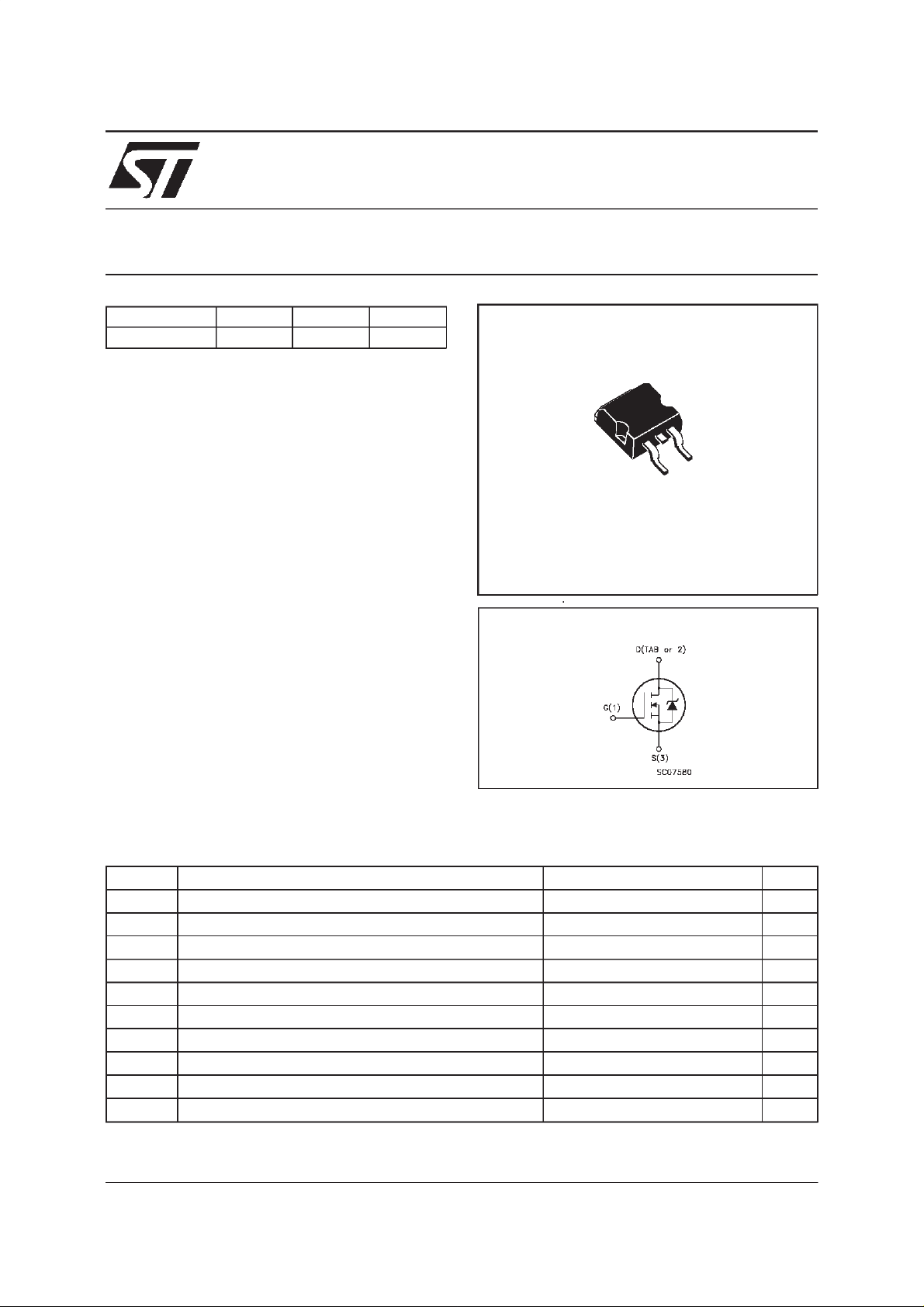
3
1
D2PAK
TO-263
(suffix ”T4”)
INTERNAL SCHEMATIC DIAGRAM
ABSOLUTE MAXIMUM RATINGS
Symb o l Parameter Val u e Uni t
V
V
V
I
DM
P
T
(•) Pulse width limited by safe operatingarea
March 1999
Drain-source Volt age (VGS=0) 30 V
DS
Drain- gate Vol ta ge (RGS=20kΩ)30V
DGR
Gate-s ource Voltage
GS
I
Drain Curr ent (c ont i nuous) at Tc=25oC40A
D
I
Drain Curr ent (c ont i nuous) at Tc= 100oC28A
D
20 V
±
(•) D rain Curr ent ( pulsed) 160 A
Total Dissipation at Tc=25oC80W
tot
Derating Fact or 0.53 W/
St orage Tem p er ature -65 to 175
stg
T
Max. O per ating Jun ction Tem p er at u re 175
j
o
C
o
C
o
C
1/8
Page 2
STB3020L
THERMAL DATA
R
thj-case
Rthj-amb
R
thc-sink
T
Ther mal Resistanc e Junct ion-case Max
Ther mal Resistanc e Junct ion-ambie nt Max
Ther mal Resistanc e Case-sink Ty p
Maximum Lead Tempe rat ur e For Soldering Purpos e
l
1.875
62.5
0.5
300
o
C/W
oC/W
o
C/W
o
C
ELECTRICAL CHARACTERISTICS
=25oC unless otherwisespecified)
(T
case
OFF
Symbol Parameter Test Conditions Min. Typ. Max. Unit
V
(BR)DSS
Drain-source
ID=250µAVGS=0 30 V
Break dow n Voltage
I
DSS
I
GSS
Zero Gate Voltage
Drain Cur re nt ( V
GS
Gat e- bod y L eakage
Current (V
DS
=0)
=0)
V
=MaxRating
DS
=MaxRating Tc=125oC
V
DS
V
= ± 20 V ± 100 nA
GS
1
10
ON (∗)
Symbol Parameter Test Conditions Min. Typ. Max. Unit
V
GS(th)
R
DS(on)
I
D(on)
Gate Threshold Voltage VDS=VGSID= 250 µA12.5V
Sta t ic Drain -s ource O n
Resistance
VGS=10V ID=20A
=5V ID=20A
V
GS
On State Drain Current VDS>I
D(on)xRDS(on)max
0.019
0.033
40 A
0.022
0.038ΩΩ
VGS=10V
DYNAMIC
Symbol Parameter Test Conditions Min. Typ. Max. Unit
g
(∗)Forward
fs
Tr ansc on duc tance
C
C
C
Input Capac i t ance
iss
Out put Capacitance
oss
Reverse Tr ansfer
rss
Capacit a nc e
VDS>I
D(on)xRDS(on)maxID
=20 A 5 20 S
VDS=25V f=1MHz VGS= 0 1270
350
115
µ
µA
pF
pF
pF
A
2/8
Page 3
STB3020L
ELECTRICAL CHARACTERISTICS
(continued)
SWITCHINGON
Symbol Parameter Test Conditions Min. Typ. Max. Unit
t
d(on)
Tur n-on Delay Time
Rise Ti me
t
r
VDD=15V ID=19A
R
=4.7
G
Ω
VGS=4.5V
28
220
(Resis t iv e Loa d, see fig. 3)
Q
Q
Q
Tot al Gat e Charge
g
Gat e- Source Char g e
gs
Gate-Drain Charge
gd
VDD=24V ID=38A VGS=5V 21
9
11
29 nC
SWITCHINGOFF
Symbol Parameter Test Conditions Min. Typ. Max. Unit
t
d(off)
Tur n-of f Delay T im e
t
Fall T ime
f
VDD=15V ID=19A
=4.7 Ω VGS=4.5V
R
G
45
35
(Resis t iv e Loa d, see fig. 3)
t
r(Voff)
t
t
Off-v oltage Rise Tim e
Fall T ime
f
Cross-over Tim e
c
VDD=24V ID=38A
=4.7 Ω VGS=4.5V
R
G
(Indu ct iv e Load , s e e fig. 5)
30
85
125
SOURCEDRAINDIODE
Symbol Parameter Test Conditions Min. Typ. Max. Unit
I
SDM
V
I
SD
Q
I
RRM
SD
t
Source-drain Current
(•)
Source-drain Current
40
160
(pulsed)
(∗)ForwardOnVoltage ISD=40A VGS=0 1.5 V
Reverse Recovery
rr
Time
Reverse Recovery
rr
ISD= 38 A di/dt = 100 A /µs
=15V Tj=150oC
V
DD
(see test circuit, fig. 5)
45
60
Charge
Reverse Recovery
2.5
Current
ns
ns
nC
nC
ns
ns
ns
ns
ns
A
A
ns
nC
A
(∗) Pulsed: Pulse duration = 300 µs, duty cycle 1.5 %
(•) Pulse width limited by safe operatingarea
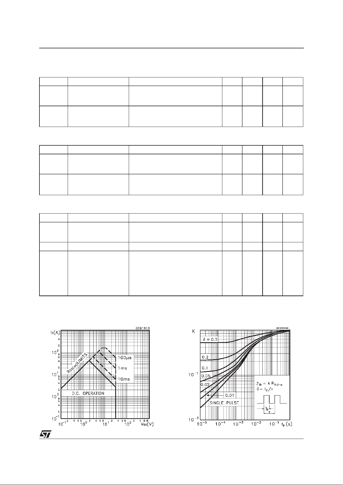
SafeOperating Area ThermalImpedance
3/8
Page 4

STB3020L
OutputCharacteristics
Transconductance
TransferCharacteristics
Static Drain-sourceOn Resistance
Gate Charge vs Gate-sourceVoltage
4/8
CapacitanceVariations
Page 5

STB3020L
NormalizedGate ThresholdVoltage vs
Temperature
Source-drainDiode Forward Characteristics
NormalizedOn Resistancevs Temperature
5/8
Page 6

STB3020L
Fig. 1: Unclamped Inductive Load Test Circuit
Fig. 3: Switching Times Test Circuits For
ResistiveLoad
Fig. 2: Unclamped InductiveWaveform
Fig. 4: Gate Chargetest Circuit
Fig. 5: Test Circuit For InductiveLoad Switching
And Diode Recovery Times
6/8
Page 7

TO-263 (D2PAK) MECHANICAL DATA
STB3020L
DIM.
MIN. TYP. MAX. MIN. TYP. MAX.
A 4.4 4.6 0.173 0.181
A1 2.49 2.69 0.098 0.106
B 0.7 0.93 0.027 0.036
B2 1.14 1.7 0.044 0.067
C 0.45 0.6 0.017 0.023
C2 1.21 1.36 0.047 0.053
D 8.95 9.35 0.352 0.368
E 10 10.4 0.393 0.409
G 4.88 5.28 0.192 0.208
L 15 15.85 0.590 0.624
L2 1.27 1.4 0.050 0.055
L3 1.4 1.75 0.055 0.068
mm inch
D
A
C2
DETAIL”A”
C
A2
DETAIL”A”
A1
B2
E
L2
L
L3
B
G
P011P6/E
7/8
Page 8

STB3020L
Information furnished is believed tobe accurate and reliable. However, STMicroelectronics assumes no responsibilityfor the consequences
of use of such information nor for any infringement of patents or other rights of third parties which may result from its use. No license is
granted by implication orotherwise under any patent or patent rights of STMicroelectronics. Specificationmentioned in this publication are
subjecttochange without notice. This publication supersedes andreplaces all information previouslysupplied. STMicroelectronicsproducts
are not authorized for use as critical components in life support devices or systemswithout express written approval of STMicroelectronics.
The STlogo is a trademark of STMicroelectronics
1999 STMicroelectronics – Printed in Italy – All Rights Reserved
STMicroelectronics GROUP OF COMPANIES
Australia - Brazil - Canada - China - France - Germany - Italy- Japan - Korea - Malaysia- Malta - Mexico - Morocco - The Netherlands -
8/8
Singapore - Spain - Sweden - Switzerland - Taiwan - Thailand - United Kingdom - U.S.A.
http://www.st.com
.
 Loading...