

Page 1
STB3015L
®
N - CHANNEL 30V - 0.013 Ω - 40A - D2PAK/TO-220
TYPE V
DSS
STB3015L 30 V < 0.0155 Ω 40 A
■ TYPICAL R
■ EXCEPTI ON AL dv/dt CAP AB ILI TY
■ LOW GATE CHARG E A 1 00
■ APPLICATION ORIENTED
DS(on)
= 0.013 Ω
CHARACTERIZATION
■ FOR THROUGH- HOLE VERSIO N
CONTACT SALES OFFICE
DESCRIPTION
This Power MOSFET is the latest development of
STMicroelectronics unique " Single Feature
Size " strip-based process. The resulting transistor shows extremely high packing density for
low on-resistance, rugged avalanche characteristics and less critical alignment steps therefore
a remarkable manufacturing reproducibility.
R
DS(on)
o
C
I
D
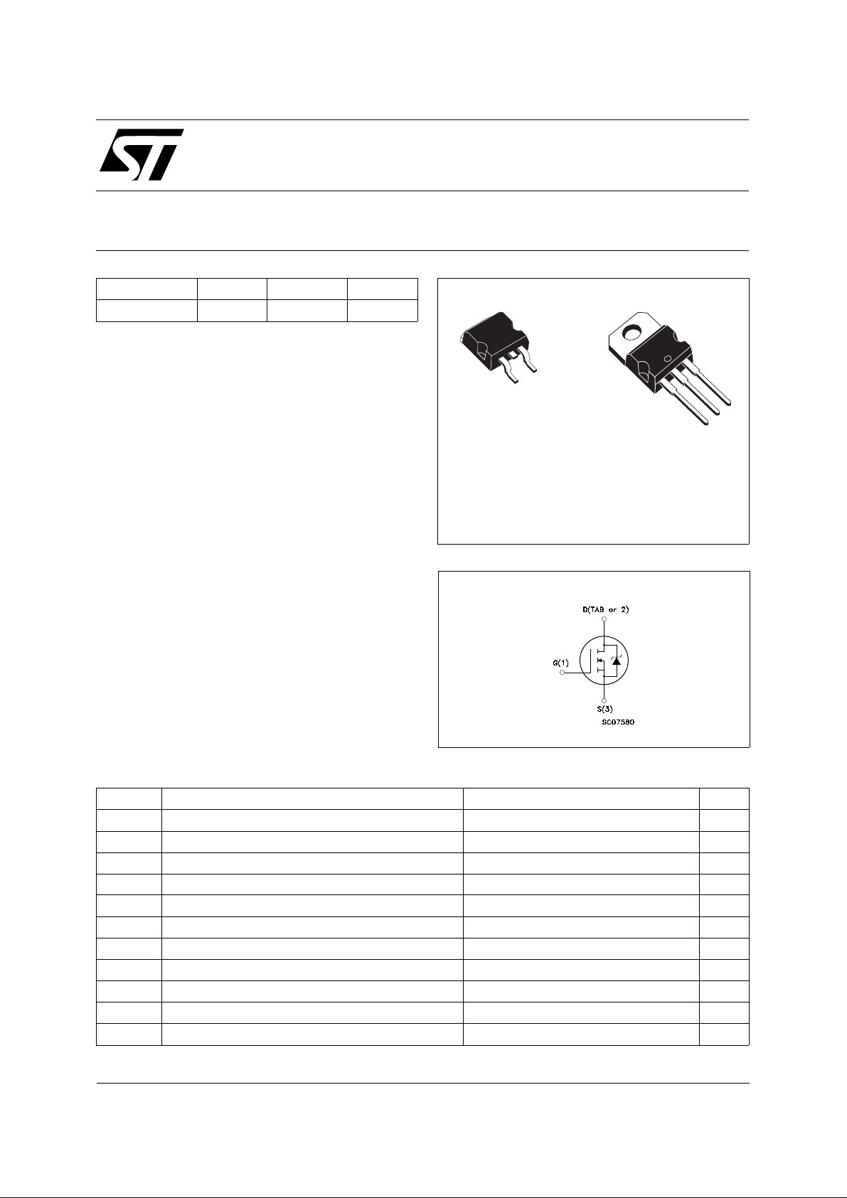
STP3015L
STripFET POWER MOSFET
PRELIMINARY DATA
3
1
D2PAK
TO-263
(Suffix "T4")
TO-220
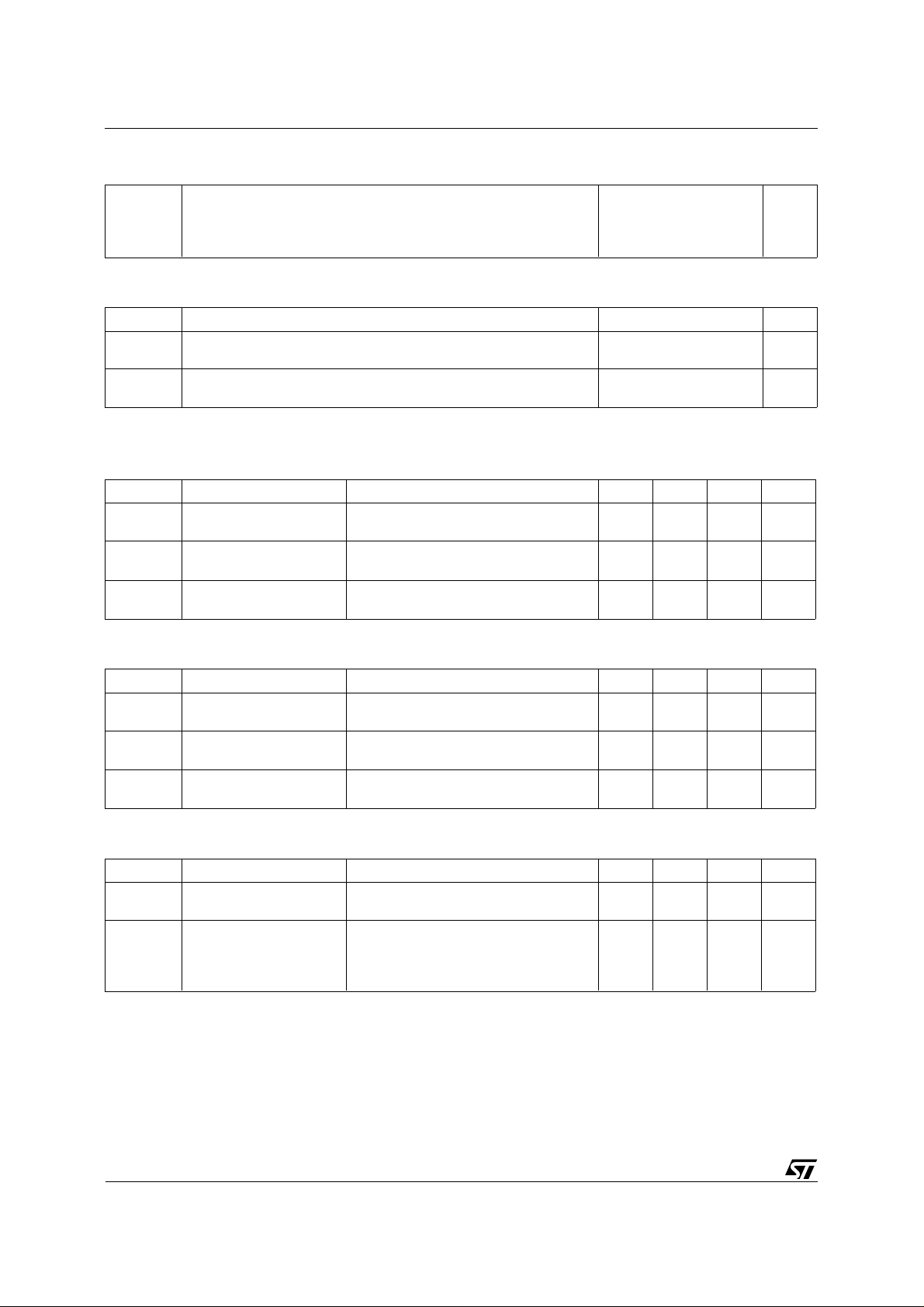
INTER NAL SCH E M ATI C DIAG RA M
3
2
1
APPLICATIONS
■ HIGH CURRENT, HIGH SPE ED SWI TCHING
SOLENOID AND RELA Y DRIVE RS
■ MOTOR CONT RO L, AUDIO AM PLIFI ER S
■ DC-DC & DC-AC CONVERT E RS IN HIGH
PERFORM A NCE VR Ms
■ AUTOMO TIV E ENV IRO NME NT (INJ ECT IO N,
ABS, AIR-BAG, LAMPDRIVERS, Etc.)
ABSOLUTE MAXIMUM RATINGS
Symbol Parameter Value Unit
V
V
V
I
DM
P
dv/dt(
T
(•) Pulse width limited by safe operating area (1) ISD ≤ 40 A, di/dt ≤ 200 A/µs, VDD ≤ V
July 1998
Drain-source Voltage (VGS = 0) 30 V
DS
Drain- gate Voltage (RGS = 20 kΩ)
DGR
Gate-source Voltage ± 20 V
GS
I
Drain Current (continuous) at Tc = 25 oC40A
D
I
Drain Current (continuous) at Tc = 100 oC28A
D
30 V
(•) Drain Current (pulsed) 160 A
Total Dissipation at Tc = 25 oC80W
tot
Derating Factor 0.53 W/oC
1) Peak Diode Recovery voltage slope 7 V/ns
Storage Temperature -65 to 175
stg
T
Max. Operating Junction Temperature 175
j
, Tj ≤ T
(BR)DSS
JMAX
o
C
o
C
1/5
Page 2
STB3015L
THERMAL DATA
R
thj-case
R
thj-amb
R
thc-si n k
T
Thermal Resistance Junction-case Max
Thermal Resistance Junction-ambient Max
Thermal Resistance Case-sink Typ
Maximum Lead Temperature For Soldering Purpose
l
AVALANCHE CHARACTERI S TICS
Symbol Parameter Max Value Unit
I
AR
E
Avalanche Current, Repetitive or Not-Repetitive
(pulse width limited by T
Single Pulse Avalanche Energy
AS
(starting T
= 25 oC, ID = IAR, V
j
ma x)
j
DD
= 15 V)
1.88
62.5
0.5
300
40 A
200 mJ
o
C/W
o
C/W
o
C/W
o
C
ELECTRICAL CHARACTERISTICS (T
= 25 oC unless otherwise specified)
case
OFF
Symbol Parameter Test Conditions Min. Typ. Max. Unit
V
(BR)DSS
Drain-source
I
= 250 µA V
D
GS
= 0
30 V
Breakdown Voltage
I
DSS
I
GSS
Zero Gate Voltage
Drain Current (V
GS
Gate-body Leakage
Current (V
DS
= 0)
= 0)
= Max Rating
V
DS
V
= Max Rating Tc = 125 oC
DS
V
= ± 20 V
GS
1
10
± 100 nA
ON (∗)
Symbol Parameter Test Conditions Min. Typ. Max. Unit
V
GS(th)
Gate Threshold
V
= VGS ID = 250 µA
DS
1 2.5 V
Voltage
R
DS(on)
I
D(on)
Static Drain-source On
Resistance
V
= 10 V ID = 20 A
GS
V
= 5 V ID = 20 A
GS
On State Drain Current VDS > I
V
= 10 V
GS
D(on)
x R
DS(on)max
0.013 0.0155
0.022ΩΩ
40 A
DYNAMIC
Symbol Parameter Test Conditions Min. Typ. Max. Unit
g
(∗) Forward
fs
Transconductance
C
C
C
Input Capacitance
iss
Output Capacitance
oss
Reverse Transfer
rss
Capacitance
VDS > I
V
DS
x R
D(on)
DS(on)max
= 25 V f = 1 MHz V
ID =20 A 15 20 S
= 0 2500
GS
1200
400
µA
µA
pF
pF
pF
2/5
Page 3

STB3015L
ELECTRICAL CHARACTERISTICS (continued)
SWITCHING O N
Symbol Parameter Test Conditions Min. Typ. Max. Unit
t
d(on)
t
r
Turn-on Time
Rise Time
V
= 15 V ID = 20 A
DD
RG = 4.7 Ω VGS = 5 V
25
160
ns
ns
Q
Total Gate Charge VDD = 24 V ID = 40 A V
g
= 5 V 40 nC
GS
SWITCHING O F F
Symbol Parameter Test Conditions Min. Typ. Max. Unit
t
r(Voff)
t
t
Off-voltage Rise Time
Fall Time
f
Cross-over Time
c
V
= 24 V ID = 40 A
DD
RG = 4.7 Ω VGS = 5 V
25
120
155
SOURCE DRAIN DIO DE
Symbol Parameter Test Conditions Min. Typ. Max. Unit
40
160
I
SDM
I
SD
Source-drain Current
(•)
Source-drain Current
(pulsed)
V
(∗) Forward On Voltage ISD = 40 A VGS = 0 1.3 V
SD
t
Q
Reverse Recovery
rr
Time
Reverse Recovery
rr
I
= 40 A di/dt = 100 A/µs
SD
V
= 20 V Tj = 150 oC
DD
50
0.9
Charge
I
RRM
Reverse Recovery
3.5
Current
(∗) Pulsed: Pulse duration = 300 µs, duty cycle 1.5 %
(•) Pulse width limited by safe operating area
ns
ns
ns
A
A
ns
nC
A
3/5
Page 4

STB3015L
TO-263 (D2PAK) MECHANICAL DATA
DIM.
MIN. TYP. MAX. MIN. TYP. MAX.
A 4.3 4.6 0.169 0.181
A1 2.49 2.69 0.098 0.106
B 0.7 0.93 0.027 0.036
B2 1.25 1.4 0.049 0.055
C 0.45 0.6 0.017 0.023
C2 1.21 1.36 0.047 0.053
D 8.95 9.35 0.352 0.368
E 10 10.28 0.393 0.404
G 4.88 5.28 0.192 0.208
L 15 15.85 0.590 0.624
L2 1.27 1.4 0.050 0.055
L3 1.4 1.75 0.055 0.068
mm inch
E
A
C2
L2
D
L
L3
B2
B
A1
C
G
P011P6/C
4/5
Page 5

E
TO-220 MECHANICAL DATA
STB3015L
DIM.
A 4.40 4.60 0.173 0.181
C 1.23 1.32 0.048 0.051
D 2.40 2.72 0.094 0.107
D1 1.27 0.050
E 0.49 0.70 0.019 0.027
F 0.61 0.88 0.024 0.034
F1 1.14 1.70 0.044 0.067
F2 1.14 1.70 0.044 0.067
G 4.95 5.15 0.194 0.203
G1 2.4 2.7 0.094 0.106
H2 10.0 10.40 0.393 0.409
L2 16.4 0.645
L4 13.0 14.0 0.511 0.551
L5 2.65 2.95 0.104 0.116
L6 15.25 15.75 0.600 0.620
L7 6.2 6.6 0.244 0.260
L9 3.5 3.93 0.137 0.154
DIA. 3.75 3.85 0.147 0.151
MIN. TYP. MAX. MIN. TYP. MAX.
mm inch
A
C
D
L5
Dia.
L7
D1
L6
L2
L9
F1
G1
H2
G
F
F2
L4
P011C
5/5
Page 6

STB3015L
Information furnished is believed to be accurate and reliable. However, STMicroelectronics assumes no responsibility for the consequences
of use of such information n or for any infrin gement of patents or othe r rights of third parties which may result from its use. No licens e i s
granted by implication or otherwise under any patent or patent rights of STMicroelectronics. Specification mentioned in this publication are
subject to change without notice. This publication supersedes and replaces all information previously supplied. STMicroelectronics products
are not authorized for use as critical components in life support devices or systems without express written approval of STMicroelectronics.
Australia - Brazil - Canada - China - France - Germany - Italy - Japan - Korea - Malaysia - Malta - Mexico - Morocco - The Netherlands -
Singapore - Spain - Sweden - Switzerland - Taiwan - Thailand - United Kingdom - U.S.A.
The ST logo is a trademark of STMicroelect ronics
© 1998 STMicroelectronics – Printed in Italy – All Rights Reserved
STMicroelectronics GROUP OF COMPANIES
.
6/5
 Loading...