

Datasheet STP22NM60, STP22NM60FP, STB22NM60, STB22NM60-1 Datasheet (SGS Thomson Microelectronics)
Page 1
1/11
ADVANCED DATA
June 2003
STP22NM60 - STF22NM60
STB22NM60 - STB22NM60-1 - STW22NM60
N-CHANNEL 600V - 0.19 Ω - 22A TO-220/FP/D2PAK/I2PAK/TO-247
MDmesh™Power MOSFET
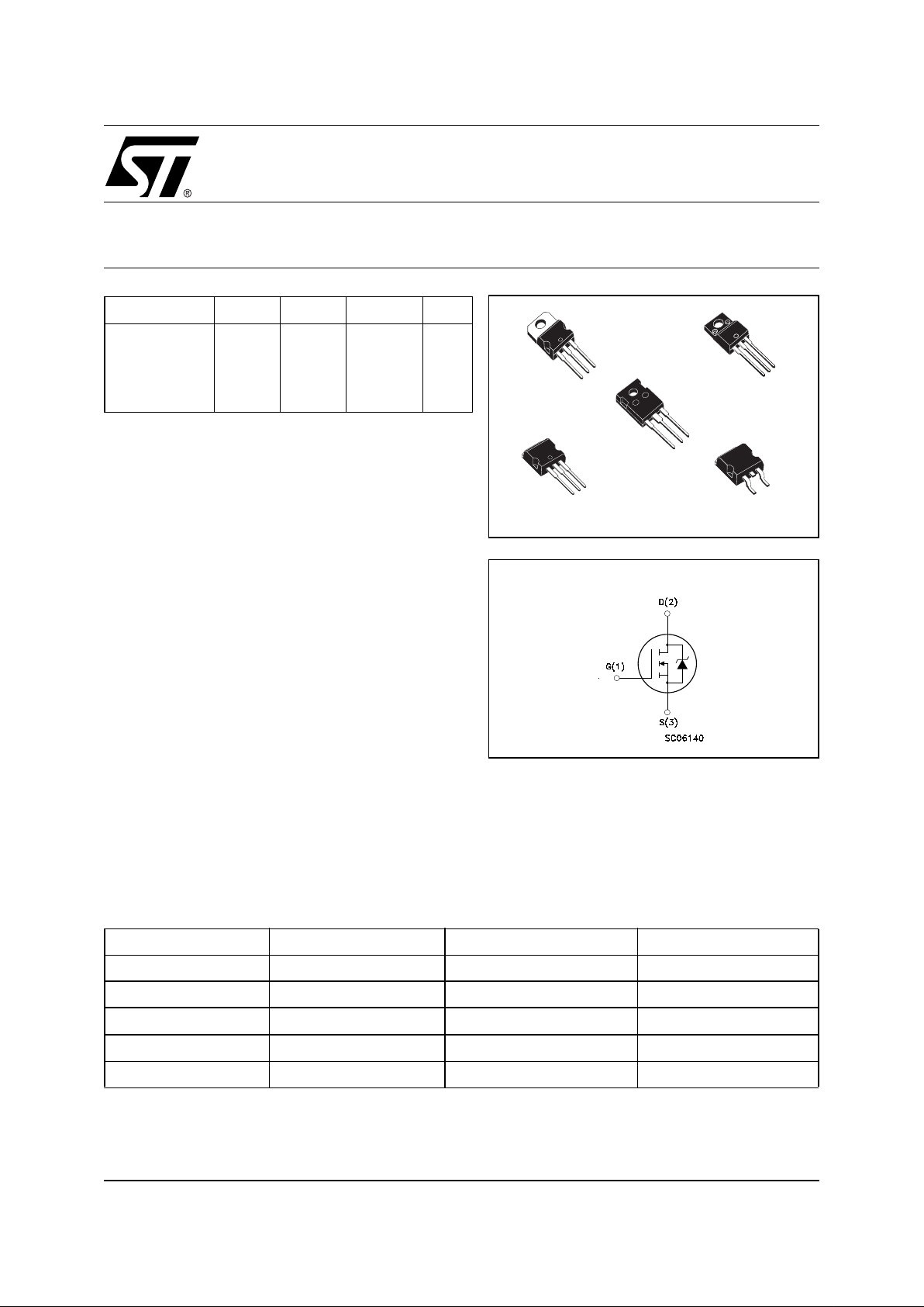
1
2
3
1
3
1
2
3
TO-220FP
I
2
PAK
D
2
PAK
1
2
3
1
2
3
TO-220
TO-247
■ TYPICAL R
DS
(on) = 0.19Ω
■ HIGH dv/dt AND AVALANCHE CAPABILITIES
■ 100% AV ALANCHE TESTED
■ LOW INPUT CAPACITANCE AND GATE CHARGE
■ LOW GATE INPUT RESISTANCE
DESCRIPTION
This improved version of MDmesh™ which is based
on Multiple Drain proc ess represents the new benchmark in high voltage MOSFETs. The resulting product
exhibits ev en lower on-resistance, impressively high
dv/dt and excellent avalanche characteristics. The
adoption of the Company’s proprietary strip technique
yields overall performances that are significantlybetter
than t hat of simi lar compet it ion’s products.
APPLICATIONS
The MDmesh™ family is very suitable for increasing
power density of high voltage converters allowing system miniaturization and higher efficiencies.
ORDERING INFORMATION
TYPE V
DSS
R
DS(on)Rds(on)*QgID
STP22NM60
STF22NM60
STB22NM60
STB22NM60-1
STW22NM60
600 V
600 V
600 V
600 V
600 V
< 0.25 Ω
< 0.25 Ω
< 0.25 Ω
< 0.25 Ω
< 0.25 Ω
7.6 Ω*nC
7.6 Ω*nC
7.6 Ω*nC
7.6 Ω*nC
7.6 Ω*nC
22 A
22 A
22 A
22 A
22 A
SALES TYPE MARKING PACKAGE PACKAGING
STP22NM60 P22NM60 TO-220 TUBE
STF22NM60 F22NM60 TO-220FP TUBE
STB22NM60
B22NM60T4 D
²PAK TAPE & REEL
STB22NM60-1
B22NM60-1 I
²PAK TUBE
STW22NM60 W22NM60 TO-247 TUBE
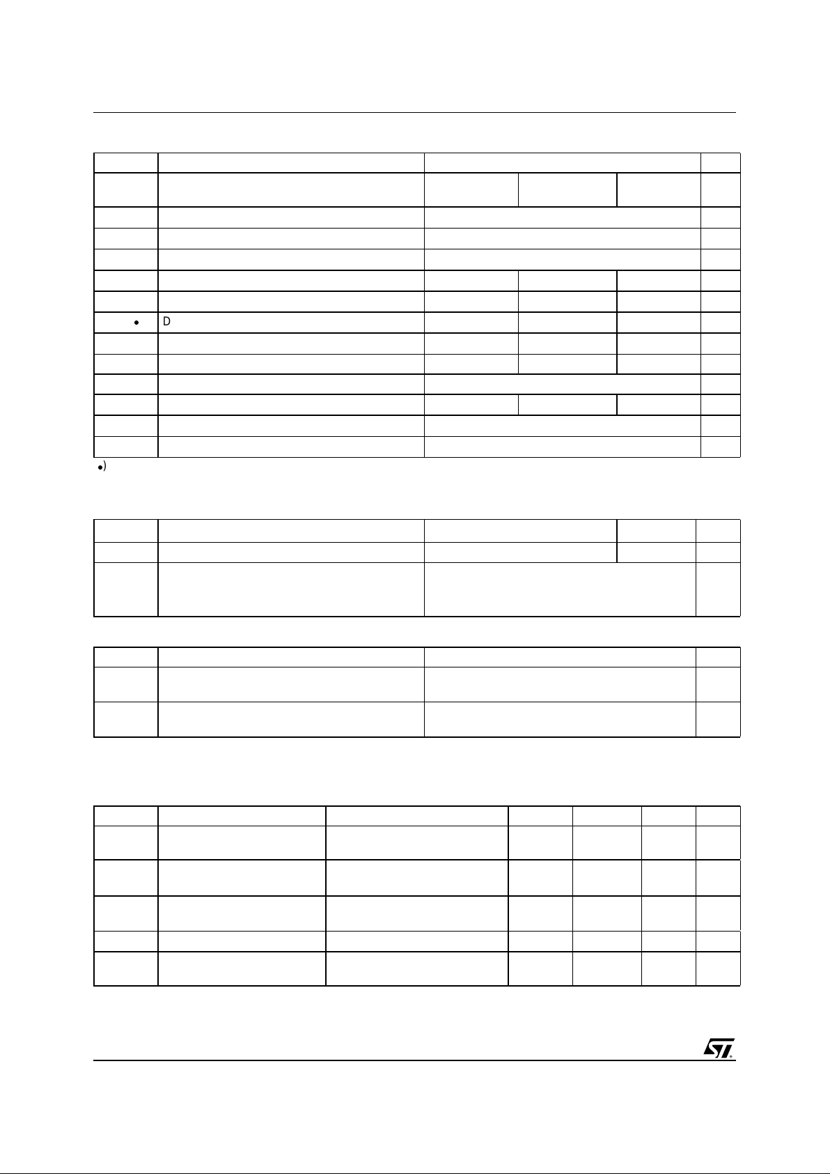
I
NTERNAL SCHEMATIC DIAGRAM
Page 2
STP22NM60 / STF22NM60 / ST B 22NM6 0 / STB22NM60-1 - STW22NM60
2/11
ABSOLUTE M AXIMUM RA TINGS
() Pulse width limited by safe operating area; (*)Limited only by maximum temperature allowed
(1) I
SD
≤22A, di/dt ≤400A/µs, VDD≤ V
(BR)DSS,Tj≤TJMAX.
THERMAL DATA
AVALANCHE CHARACTERISTICS
ELECTRICAL CHARACT ERISTICS (T
CASE
= 25 °C UNLESS OTHERWISE SPECIFIED)
ON/OFF
Symbol Parameter Value Unit
STP22NM60
STB22NM60/1
STF22NM60 STW22NM60
V
DS
Drain-source Voltage (VGS=0)
600 V
V
DGR
Drain-gate Voltage (RGS=20kΩ)
600 V
V
GS
Gate- source Voltage ±30 V
I
D
Drain Current (continuous) at TC= 25°C
22 22 (*) 22 A
I
D
Drain Current (continuous) at TC= 100°C
12.6 12.6 (*) 12.6 A
I
DM
()
Drain Current (pulsed) 80 80(*) 80 A
P
TOT
Total Dissipation at TC= 25°C
192 45 210 W
Derating Factor 1.2 0.36 1.2 W/°C
dv/dt(1) Peak Diode Recovery voltage slope 15 V/ns
V
ISO
Insulation Winthstand Voltage (DC) -- 2500 -- V
T
stg
Storage Temperature –65 to 150 °C
T
j
Max. Operating Junction Temperature 150 °C
TO-220/D
2
PAK/I2PAK/TO-247
TO-220FP
Rthj-case ThermalResistanceJunction-case Max 0.65 2.8 °C/W
Rthj-amb ThermalResistanceJunction-ambient Max 62.5 °C/W
T
l
Maximum Lead Temperature For Soldering
Purpose
300 °C
Symbol Parameter Max Value Unit
I
AR
Avalanche Current, Repetitive or Not-Repetitive
(pulse width limited by T
j
max)
11 A
E
AS
Single Pulse Avalanche Energy
(starting T
j
=25°C,ID=IAR,VDD=50V)
650 mJ
Symbol Parameter Test Conditions Min. Typ. Max. Unit
V
(BR)DSS
Drain-source
Breakdown Voltage
ID= 250 µA, VGS=0 600 V
I
DSS
Zero Gate Voltage
Drain Current (V
GS
=0)
V
DS
= Max Rating
V
DS
= Max Rating, TC=125°C
1
10
µA
µA
I
GSS
Gate-body Leakage
Current (V
DS
=0)
V
GS
= ±30 V ±100 nA
V
GS(th)
Gate Threshold Voltage
V
DS=VGS,ID
= 250 µA
34
5V
R
DS(on)
Static Drain-source On
Resistance
VGS=10V,ID= 11 A 0.19 0.25 Ω
Page 3
3/11
STP22NM60 / STF22NM60 / STB22NM60 / STB22NM60-1 - STW22NM60
ELECTRICAL CHARACT ERISTICS (CO NTINUE)
DYNAMIC
(1) Pulsed: Pulse duration = 300 µs, duty cycle 1.5 %.
(*) C
oss eq.
is defined as a constant equivalent capacitance giving the same charging time as C
oss
when VDSincreases from 0 to 80% V
DSS
.
SWITCHING ON
SWITCHING OFF
SOURCE DRAIN DIODE
Note: 1. Pulsed: Pulse duration = 300 µs, duty cycle 1.5 %.
2. Pulse width limited by safe operating area.
Symbol Parameter Test Conditions Min. Typ. Max. Unit
g
fs
(1) Forward Transconductance VDS>I
D(on)xRDS(on)max,
ID=11A
TBD S
C
iss
C
oss
C
rss
Input Capacitance
Output Capacitance
Reverse Transfer
Capacitance
V
DS
=25V,f=1MHz,VGS= 0 1590
803
52
pF
pF
pF
C
oss eq.
(2) Equivalent Output
Capacitance
VGS=0V,VDS= 0V to 400V 130 pF
R
g
Gate Input Resistance f=1 MHz Gate DC Bias=0
Test Signal Level=20mV
Open Drain
1.6 Ω
Symbol Parameter Test Conditions Min. Typ. Max. Unit
t
d(on)
t
r
Turn-on Delay Time
Rise Time
VDD=200V,ID=11A
R
G
= 4.7Ω VGS=10V
(see test circuit, Figure 3)
25
20
ns
ns
Q
g
Q
gs
Q
gd
Total Gate Charge
Gate-Source Charge
Gate-Drain Charge
VDD=400V,ID=22A,
VGS=10V
40
11
25
71
nC
nC
nC
Symbol Parameter Test Conditions Min. Typ. Max. Unit
t
r(Voff)
Off-voltage Rise Time
V
DD
= 480 V, ID=22A,
RG=4.7Ω, VGS=10V
(see test circuit, Figure 5)
13 ns
t
f
Fall Time 15 ns
t
c
Cross-over Time 26 ns
Symbol Parameter Test Conditions Min. Typ. Max. Unit
I
SD
Source-drain Current 20 A
I
SDM
(2)
Source-drain Current (pulsed) 80 A
V
SD
(1)
Forward On Voltage
ISD=22A,VGS=0
1.5 V
t
rr
Q
rr
I
rrm
Reverse Recovery Time
Reverse Recovery Charge
Reverse Recovery Current
I
SD
= 22 A, di/dt = 100 A/µs,
VDD=100V,Tj=25°C
(see test circuit, Figure 5)
416
5.6
27
ns
µC
A
t
rr
Q
rr
I
rrm
Reverse Recovery Time
Reverse Recovery Charge
Reverse Recovery Current
I
SD
= 22 A, di/dt = 100 A/µs,
V
DD
=100V,Tj=150°C
(see test circuit, Figure 5)
544
7.3
28
ns
µC
A
Page 4

STP22NM60 / STF22NM60 / ST B 22NM6 0 / STB22NM60-1 - STW22NM60
4/11
Fig. 5: Test Circuit For Inductive Load Switching
And Diode Recovery Times
Fig. 4: Gate Charge test Circuit
Fig. 2: Unclamped Inductive WaveformFig. 1: Unclamped Inductive Load Test Circuit
Fig. 3: Switching Times Test Circuit For
Resistive Load
Page 5

5/11
STP22NM60 / STF22NM60 / STB22NM60 / STB22NM60-1 - STW22NM60
DIM.
mm inch
MIN. TYP. MAX. MIN. TYP. MAX.
A 4.40 4.60 0.173 0.181
C 1.23 1.32 0.048 0.051
D 2.40 2.72 0.094 0.107
D1 1.27 0.050
E 0.49 0.70 0.019 0.027
F 0.61 0.88 0.024 0.034
F1 1.14 1.70 0.044 0.067
F2 1.14 1.70 0.044 0.067
G 4.95 5.15 0.194 0.203
G1 2.4 2.7 0.094 0.106
H2 10.0 10.40 0.393 0.409
L2 16.4 0.645
L4 13.0 14.0 0.511 0.551
L5 2.65 2.95 0.104 0.116
L6 15.25 15.75 0.600 0.620
L7 6.2 6.6 0.244 0.260
L9 3.5 3.93 0.137 0.154
DIA. 3.75 3.85 0.147 0.151
L6
A
C
D
E
D1
F
G
L7
L2
Dia.
F1
L5
L4
H2
L9
F2
G1
TO-220 MECHANICAL DATA
P011C
Page 6

STP22NM60 / STF22NM60 / ST B 22NM6 0 / STB22NM60-1 - STW22NM60
6/11
L2
A
B
D
E
H
G
L6
F
L3
G1
123
F2
F1
L7
L4
L5
DIM.
mm. inch
MIN. TYP MAX. MIN. TYP. MAX.
A 4.4 4.6 0.173 0.181
B 2.5 2.7 0.098 0.106
D 2.5 2.75 0.098 0.108
E 0.45 0.7 0.017 0.027
F 0.75 1 0.030 0.039
F1 1.15 1.7 0.045 0.067
F2 1.15 1.7 0.045 0.067
G 4.95 5.2 0.195 0.204
G1 2.4 2.7 0.094 0.106
H 10 10.4 0.393 0.409
L2 16 0.630
L3 28.6 30.6 1.126 1.204
L4 9.8 10.6 .0385 0.417
L5 2.9 3.6 0.114 0.141
L6 15.9 16.4 0.626 0.645
L7 9 9.3 0.354 0.366
Ø 3 3.2 0.118 0.126
TO-220FP MECHANICAL DATA
Page 7

7/11
STP22NM60 / STF22NM60 / STB22NM60 / STB22NM60-1 - STW22NM60
1
DIM.
mm. inch
MIN. TYP MAX. MIN. TYP. MAX.
A 4.4 4.6 0.173 0.181
A1 2.49 2.69 0.098 0.106
A2 0.03 0.23 0.001 0.009
B 0.7 0.93 0.027 0.036
B2 1.14 1.7 0.044 0.067
C 0.45 0.6 0.017 0.023
C2 1.23 1.36 0.048 0.053
D 8.95 9.35 0.352 0.368
D1 8 0.315
E 10 10.4 0.393
E1 8.5 0.334
G 4.88 5.28 0.192 0.208
L 15 15.85 0.590 0.625
L2 1.27 1.4 0.050 0.055
L3 1.4 1.75 0.055 0.068
M 2.4 3.2 0.094 0.126
R 0.4 0.015
V2 0º 8º
D2PAK MECHANICAL DATA
3
Page 8

STP22NM60 / STF22NM60 / ST B 22NM6 0 / STB22NM60-1 - STW22NM60
8/11
DIM.
mm inch
MIN. TYP. MAX. MIN. TYP. MAX.
A 4.4 4.6 0.173 0.181
A1 2.49 2.69 0.098 0.106
B 0.7 0.93 0.027 0.036
B2 1.14 1.7 0.044 0.067
C 0.45 0.6 0.017 0.023
C2 1.23 1.36 0.048 0.053
D 8.95 9.35 0.352 0.368
e 2.4 2.7 0.094 0.106
E 10 10.4 0.393 0.409
L 13.1 13.6 0.515 0.531
L1 3.48 3.78 0.137 0.149
L2 1.27 1.4 0.050 0.055
L
L1
B2
B
D
E
A
C2
C
A1
L2
e
P011P5/E
TO-262 (I2PAK) MECHANICAL DATA
Page 9

9/11
STP22NM60 / STF22NM60 / STB22NM60 / STB22NM60-1 - STW22NM60
TAPE AND REEL SHIPMENT (suffix ”T4”)*
TUBE SHIPMENT (no suffix)*
D2PAK FOOTPRINT
* on sales t y pe
DIM.
mm inch
MIN. MAX. MIN. MAX.
A 330 12.992
B 1.5 0.059
C 12.8 13.2 0.504 0.520
D 20.2 0795
G 24.4 26.4 0.960 1. 039
N 100 3.937
T 30.4 1.197
BASE QT Y BULK QTY
1000 1000
REEL MECHANICAL DATA
DIM.
mm inch
MIN. MAX. MIN. MAX.
A0 10.5 10.7 0.413 0.421
B0 15.7 15.9 0.618 0 .626
D 1.5 1.6 0.059 0.063
D1 1.59 1.61 0.062 0.063
E 1.65 1.85 0.065 0.073
F 11.4 11.6 0.449 0.456
K0 4.8 5.0 0.189 0.197
P0 3.9 4.1 0.153 0.161
P1 11.9 12.1 0.468 0.476
P2 1.9 2.1 0.075 0.082
R 50 1.574
T 0.25 0.35 0.0098 0.0137
W 23.7 24.3 0.933 0.956
TAPE MECHANICAL DATA
Page 10

STP22NM60 / STF22NM60 / ST B 22NM6 0 / STB22NM60-1 - STW22NM60
10/11
DIM.
mm. inch
MIN. TYP MAX. MIN. TYP. MAX.
A 4.85 5.15 0.19 0.20
A1 2.20 2.60 0.086 0.102
b 1.0 1.40 0.039 0.055
b1 2.0 2.40 0.079 0.094
b2 3.0 3.40 0.118 0.134
c 0.40 0.80 0.015 0.03
D 19.85 20.15 0.781 0.793
E 15.45 15.75 0.608 0.620
e5.45 0.214
L 14.20 14.80 0.560 0.582
L1 3.70 4.30 0.14 0.17
L2 18.50 0.728
øP 3.55 3.65 0.140 0.143
øR 4.50 5.50 0.177 0.216
S5.50 0.216
TO-247 MECHANICAL DATA
Page 11

11/11
STP22NM60 / STF22NM60 / STB22NM60 / STB22NM60-1 - STW22NM60
Information furnished is believed to be accurate and reliable. However, STMicroelectronics assumes no responsibility for the
consequences of u se of such inf ormat ion nor for any in fring ement of p aten ts or othe r ri ghts of th ird p arties whic h may resul t f rom
its use. No license is granted by implication or otherwise under any patent or patent rights of STMicroelectronics. Specifications
mentioned in this publication are subject to change without notice. This publication supersedes and replaces all information
previously supplied. STMicroelectronics products are not authorized for use as critical components in life support devices or
systems without express written approval of STMicroelectronics.
© The ST logo is a registered trademark of STMicroelectronics
© 2003 STMicroelectronics - Printed in Italy - All Rights Reserved
STMicroelectronics GROUP OF COMPANIES
Australia - Brazil - Canada - China - Finland - France - Germany - Hong Kong - India - Israel - Italy - Japan - Malaysia - Malta - Morocco
Singapore - Spain - Sweden - Switzerland - United Kingdom - United States.
© http://www.st.com
 Loading...