

Page 1
STB22NE03L
N - CHANNEL 30V - 0.034Ω - 22A TO-263
STripFET POWER MOSFET
PRELIMINARY DATA
■ TYPICALR
DS(on)
= 0.034 Ω
■ EXCEPTIONALdv/dtCAPABILITY
■ 100%AVALANCHETESTED
■ LOW GATE CHARGE AT 100
o
C
■ APPLICATIONORIENTED
CHARACTERIZATION
■ ADDSUFFIX ”T4” FORORDERING INTAPE
& REEL
DESCRIPTION
This Power MOSFET is the latest developmentof
STMicroelectronics unique ”Single Feature
Size” strip-based process. The resulting
transistor shows extremely high packing density
for low on-resistance, rugged avalanche
characteristics and less critical alignment steps
therefore a remarkable manufacturing
reproducibility.
APPLICATIONS
■ HIGHCURRENT, HIGH SPEEDSWITCHING
■ SOLENOIDAND RELAY DRIVERS
■ MOTORCONTROL, AUDIOAMPLIFIERS
■ DC-DC& DC-AC CONVERTERS
■ AUTOMOTIVEENVIRONMENT
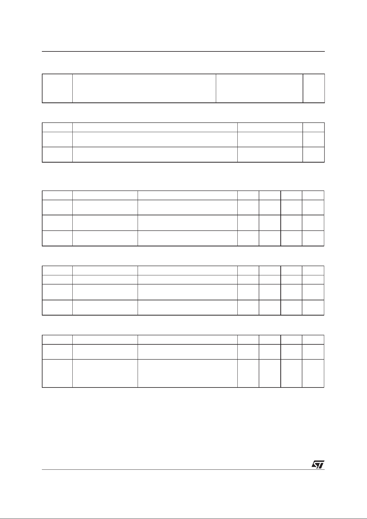
INTERNAL SCHEMATIC DIAGRAM
April 1999
1
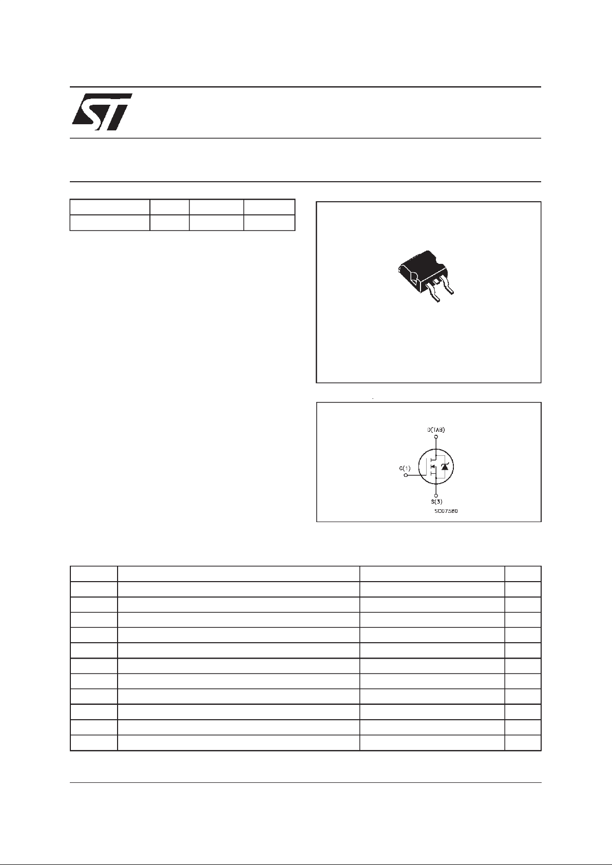
3
D2PAK
TO-263
(suffix ”T4”)
ABSOLUTE MAXIMUM RATINGS
Symbol Parameter Value Unit
V
DS
Dra in- sour c e Volt age (VGS=0) 30 V
V
DGR
Dra in- gat e Voltage (RGS=20kΩ)30V
V
GS
Gat e-source Voltage ± 15 V
I
D
Dra in Cu rr ent (continuous) at Tc=25oC22A
I
D
Dra in Cu rr ent (continuous) at Tc=100oC16A
I
DM
(•) D rain Current (pulsed ) 88 A
P
tot
Tot al Dissipat ion at Tc=25oC60W
Der ati ng Fact or 0.4 W/
o
C
dv/dt (
1) Peak Diode Recovery volt age slope 6 V/ns
T
stg
St orage Tempe rat ure -65 to 175
o
C
T
j
Max. Operating Junc t ion Temper at ure 175
o
C
(•) Pulse width limited by safe operating area (1)ISD≤ 22 A, di/dt ≤ 300 A/µs, VDD≤ V
(BR)DSS,Tj≤TJMAX
TYPE V
DSS
R
DS(on)
I
D
ST B22NE03L 30 V <0.05 Ω 22 A
1/6
Page 2
THERMAL DATA
R
thj-case
Rthj-a mb
R
thc-sink
T
l
Ther mal Resistanc e Junct ion-case Max
Ther mal Resistanc e Junct ion-ambie nt Max
Ther mal Resistanc e Case-sink Ty p
Maximum Lead Tempe rat ur e F or S o ldering Purpos e
2.5
62.5
0.5
300
o
C/W
oC/W
o
C/W
o
C
AVALANCHE CHARACTERISTICS
Symbol Parameter Max Valu e Un it
I
AR
Avalanche Current, R epetitive or Not-Repetitive
(pulse width limited by T
j
max)
22 A
E
AS
Single Pul se Avalanc he E nergy
(starting T
j
=25oC, ID=IAR,VDD=15V)
TBD mJ
ELECTRICAL CHARACTERISTICS
(T
case
=25oC unless otherwisespecified)
OFF
Symbol Parameter Test Condit ions Min. Typ. Max. U nit
V
(BR)DSS
Drain-source
Break dow n Vo lt age
ID=250µAVGS=0 30 V
I
DSS
Zero Gate Volta ge
Drain Curre nt (V
GS
=0)
V
DS
=MaxRating
V
DS
=MaxRating Tc= 125oC
1
10
µ
A
µA
I
GSS
Gat e- bod y Leakag e
Current (V
DS
=0)
V
GS
=± 15 V
±
100 nA
ON(∗)
Symbol Parameter Test Condit ions Min. Typ. Max. U nit
V
GS(th)
Gate Threshold Voltage VDS=VGSID= 250 µA11.72.5V
R
DS(on)
Sta t ic Drain-s our c e On
Resistance
VGS=10V ID=11A
V
GS
=5V ID=11A
0.034
0.049
0.05
0.06
Ω
Ω
I
D(on)
On State Drain Current VDS>I
D(on)xRDS(on)max
VGS=10V
22 A
DYNAMIC
Symbol Parameter Test Condit ions Min. Typ. Max. U nit
g
fs
(∗)Forward
Tr ansc on duc tance
VDS>I
D(on)xRDS(on)maxID
=11 A 7 13 S
C
iss
C
oss
C
rss
Input Capaci t ance
Out put Capac it anc e
Reverse Transfer
Capacit a nc e
VDS=25V f=1MHz VGS= 0 680
160
60
pF
pF
pF
STB22NE03L
2/6
Page 3

ELECTRICAL CHARACTERISTICS
(continued)
SWITCHING ON
Symbol Parameter Test Condit ions Min. Typ. Max. U nit
t
d(on)
t
r
Tur n-on Delay T ime
Rise Time
VDD=15V ID=11A
R
G
=4.7
Ω
VGS=5V
(Resis t iv e Load, see fig. 3)
15
70
ns
ns
Q
g
Q
gs
Q
gd
Tot al Gate Charge
Gat e- Source Charge
Gate-Drain Charge
VDD=24V ID=22A VGS=5V 13
6
6
18 nC
nC
nC
SWITCHING OFF
Symbol Parameter Test Condit ions Min. Typ. Max. U nit
t
r(Voff)
t
f
t
c
Off-voltage Rise Time
Fall T ime
Cross-over Time
V
clamp
=24V ID=22A
R
G
=4.7 Ω VGS=5V
(Indu ct ive L oad, see f ig. 5)
13
33
55
ns
ns
ns
SOURCE DRAIN DIODE
Symbol Parameter Test Conditions Min. Typ. Max. Unit
I
SD
I
SDM
(•)
Sou rc e-d rai n Cur re nt
Sou rc e-d rai n Cur re nt
(pulsed)
22
88
A
A
V
SD
(∗)ForwardOnVoltage ISD=22A VGS=0 1.5 V
t
rr
Q
rr
I
RRM
Reverse Recovery
Time
Reverse Recovery
Charge
Reverse Recovery
Current
ISD= 22 A di/dt = 100 A /µs
V
DD
=15V Tj=150oC
(s ee t est c irc uit , fig . 5 )
40
44
2.2
ns
µ
C
A
(∗) Pulsed: Pulse duration = 300 µs, duty cycle 1.5 %
(•) Pulse width limited by safe operating are a
STB22NE03L
3/6
Page 4

Fig. 1:
UnclampedInductiveLoad Test Circuit
Fig. 3: SwitchingTimes Test Circuits For
ResistiveLoad
Fig. 2:
UnclampedInductive Waveform
Fig. 4: Gate Chargetest Circuit
Fig. 5:
Test CircuitFor InductiveLoad Switching
And Diode Recovery Times
STB22NE03L
4/6
Page 5

DIM.
mm inch
MIN. TYP. MAX. MIN. TYP. MAX.
A 4.4 4.6 0.173 0.181
A1 2.49 2.69 0.098 0.106
B 0.7 0.93 0.027 0.036
B2 1.14 1.7 0.044 0.067
C 0.45 0.6 0.017 0.023
C2 1.21 1.36 0.047 0.053
D 8.95 9.35 0.352 0.368
E 10 10.4 0.393 0.409
G 4.88 5.28 0.192 0.208
L 15 15.85 0.590 0.624
L2 1.27 1.4 0.050 0.055
L3 1.4 1.75 0.055 0.068
L2
L3
L
B2
B
G
E
A
C2
D
C
A1
DETAIL”A”
DETAIL”A”
A2
P011P6/E
TO-263 (D2PAK) MECHANICAL DATA
STB22NE03L
5/6
Page 6

Information furnishedis believed tobeaccurateand reliable. However, STMicroelectronics assumes no responsibilityfor the consequences
of use of such information nor for any infringement of patents or other rights of third parties which may result from its use. No license is
granted by implication or otherwise under any patent or patent rights of STMicroelectronics. Specificationmentioned in this publication are
subjecttochange without notice.This publication supersedes and replaces all information previouslysupplied.STMicroelectronics products
are not authorized for use as critical components in lifesupport devices or systemswithout express written approval of STMicroelectronics.
The STlogo is a trademark of STMicroelectronics
1999 STMicroelectronics – Printed in Italy – All Rights Reserved
STMicroelectronics GROUP OF COMPANIES
Australia - Brazil - Canada - China - France - Germany - Italy- Japan - Korea - Malaysia - Malta - Mexico - Morocco - The Netherlands -
Singapore - Spain - Sweden - Switzerland - Taiwan - Thailand - United Kingdom - U.S.A.
http://www.st.com
.
STB22NE03L
6/6
 Loading...