

Page 1
STB20NM50FD
N-CHANNEL 500V - 0.20Ω - 20A D2PAK
FDmesh™Power MOSFET (With FAST DIODE)
PRELIMINARY DATA
TYPE V
STB20NM50FD 500V < 0.25Ω 20 A
n
TYPICAL RDS(on) = 0.20Ω
n
HIGH dv/dt AND AVALANCHE CAPABILITIES
n
100% AVALANCHE TESTED
n
LOW INPUT CAPACITANCE AND GATE
DSS
R
DS(on)
I
D
CHARGE
n
LOW GATE INPUT RESIST ANC E
n
TIGHT PROCESS CONTROL AND HIGH
MANUFACTURING YIELDS
DESCRIPTION
The FDmesh™
associates all advantages of re-
duced on-resistance and fast swi tching with an intrinsic fast-recovery body diode. It is therefore
strongly recommended for bridge topologies, in particular ZVS phase-shift converters.
APPLICATIONS
n
ZVS PHASE-SHIFT FULL BRIDGE
CONVERTERS FOR SMPS AND WELDING
EQUIPMENT
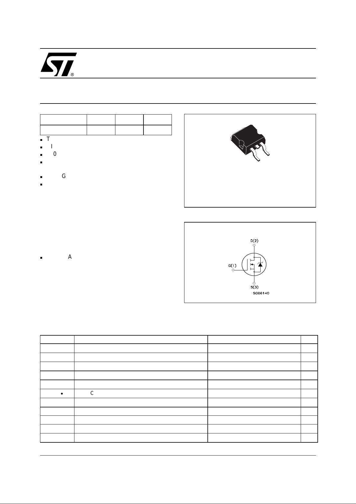
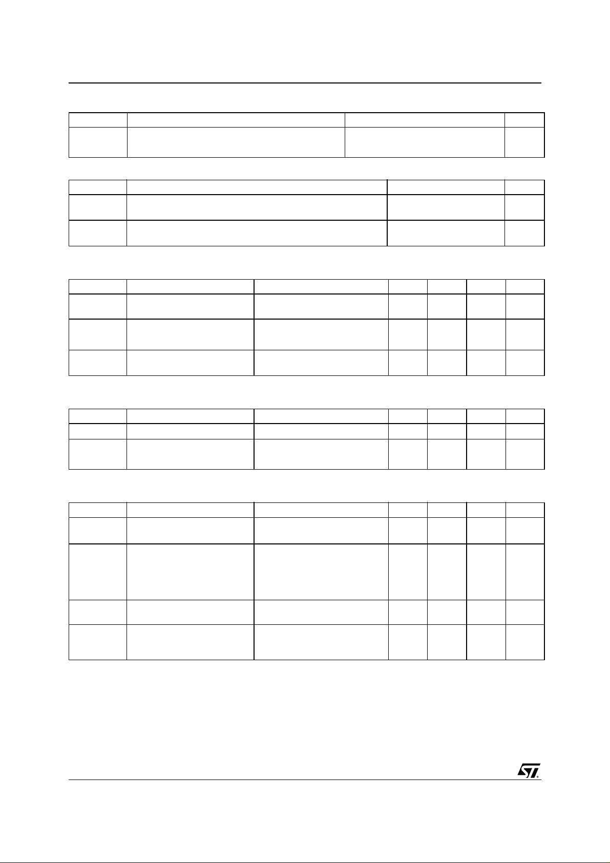
3
1
D2PAK
INTERNAL SCHEMATIC DIAGRAM
ABSOLUTE MAXIMUM RATINGS
Symbol Parameter Value Unit
V
DS
V
DGR
V
GS
I
D
I
D
I
DM
P
TOT
dv/dt Peak Diode Recovery voltage slope 6 V/ns
T
stg
T
j
(•)Pu l se width limited by safe operating area
November 2001
Drain-source Voltage (VGS = 0)
Drain-gate Voltage (RGS = 20 kΩ)
Gate- source Voltage ±30 V
Drain Current (continuos) at TC = 25°C
Drain Current (continuos) at TC = 100°C
(l)
Drain Current (pulsed) 80 A
Total Dissipation at TC = 25°C
Derating Factor 0.88 W/°C
Storage Temperature –65 to 150 °C
Max. Operating Junction Temperature 150 °C
500 V
500 V
20 A
14 A
192 W
1/7
Page 2
STB20NM50FD
THERMA L D ATA
Rthj-case Thermal Resistance Junction-case Max 0.65 °C/W
Rthj-amb Thermal Resistance Junction-ambient Max 62.5 °C/W
T
l
AVALANCHE CHARACTERISTICS
Symbol Parameter Max Value Unit
I
AR
E
AS
ELECTRICAL CHARACTERISTICS (TCASE = 25 °C UNLESS OTHERWISE SPECIFIED)
OFF
Symbol Parameter Test Conditions Min. Typ. Max. Unit
V
(BR)DSS
I
DSS
I
GSS
Maximum Lead Temperature For Soldering Purpose 300 °C
Avalanche Current, Repetitive or Not-Repetitive
(pulse width limited by T
max)
j
Single Pulse Avalanche Energy
(starting T
Drain-source
= 25 °C, ID = IAR, VDD = 35 V)
j
ID = 250 µA, VGS = 0 500 V
10 A
700 mJ
Breakdown Voltage
Zero Gate Voltage
Drain Current (V
GS
Gate-body Leakage
Current (V
DS
= 0)
= 0)
V
= Max Rating
DS
V
= Max Rating, TC = 125 °C
DS
V
= ±30V ±100 nA
GS
1µA
100 µA
ON
(1)
Symbol Parameter Test Conditions Min. Typ. Max. Unit
V
GS(th)
R
DS(on)
Gate Threshold Voltage
Static Drain-source On
V
= VGS, ID = 250µA
DS
VGS = 10V, ID = 10A
345V
0.20 0.25 Ω
Resistance
DYNAMIC
Symbol Parameter Test Conditions Min. Typ. Max. Unit
(1) Forward Transconductance VDS > I
g
fs
C
iss
C
oss
C
rss
C
oss eq.
Input Capacitance
Output Capacitance 285 pF
Reverse Transfer
Capacitance
(2) Equivalent Output
Capacitance
R
G
1. Pulsed: Pu l se duration = 300 µs, duty c yc l e 1.5 %.
2. C
Gate Input Resistance f=1 MHz Gate DC Bias = 0
is defined as a constant equivalent capacitance giving the same charging time as C
oss eq.
V
.
DSS
I
= 10A
D
V
DS
VGS = 0V, VDS = 0V to 400V 130 pF
Test Signal Level = 20mV
Open Drain
D(on)
x R
DS(on)max,
= 25V, f = 1 MHz, VGS = 0
9S
1480 pF
34 pF
1.7 Ω
when VDS increase s fr om 0 to 80%
oss
2/7
Page 3
STB20NM50FD
ELECTRICAL CHARACTERISTICS (CONTINUED)
SWITCHING ON
Symbol Parameter Test Conditions Min. Typ. Max. Unit
V
t
d(on)
Q
Q
Q
t
r
g
gs
gd
Turn-on Delay Time
Rise Time 16 ns
Total Gate Charge
Gate-Source Charge 13 nC
Gate-Drain Charge 19 nC
SWITCHING OFF
Symbol Param eter Test Conditions Min. Typ. Max. Unit
t
r(Voff)
t
f
t
c
Off-voltage Rise Time
Fall Time 8.5 ns
Cross-over Time 23 ns
SOURCE DRAIN DIODE
Symbol Parameter Test Conditions Min. Typ. Max. Unit
I
SD
I
SDM
VSD (1)
t
rr
Q
rr
I
RRM
Note: 1. Pulsed: Pulse duration = 300 µs, duty cycle 1.5 %.
2. Pulse width lim i t ed by safe ope rat i ng area.
(2)
Source-drain Current 20 A
Source-drain Current (pulsed) 80 A
Forward On Voltage
Reverse Recovery Time
Reverse Recovery Charg e 1.6 µC
Reverse Recovery Curren t 15 A
= 250V, ID = 10A
DD
RG= 4.7Ω VGS = 10V
(see test circuit, Figure 3)
V
= 400V, ID = 20A,
DD
V
= 10V
GS
V
= 400V, ID = 20A,
DD
RG= 4.7Ω, V
GS
= 10V
(see test circuit, Figure 5)
ISD = 20A, VGS = 0
I
= 20A, di/dt = 100A/µs,
SD
V
= 50V
DD
(see test circuit, Figure 5)
24 ns
40 56 nC
9ns
1.5 V
220 ns
3/7
Page 4

STB20NM50FD
Fig. 2: Unclamped Inductive WaveformFig. 1: Unclamped Inductive Load Test Circuit
Fig. 3: Switching Times Test Circuit For
Resistive Load
Fig. 5: Test Circuit For Inductive Load Switching
And Diode Recovery Times
Fig. 4: Gate Charge test Circuit
4/7
Page 5

2
D
PAK MECHA NICAL DATA
STB20NM50FD
DIM.
MIN. TYP MAX. MIN. TYP. MAX.
A 4.4 4.6 0.173 0.181
A1 2.49 2.69 0.098 0.106
A2 0.03 0.23 0.001 0.009
B 0.7 0.93 0.027 0.036
B2 1.14 1.7 0.044 0.067
C 0.45 0.6 0.017 0.023
C2 1.23 1.36 0.048 0.053
D 8.95 9.35 0.352 0.368
D1 8 0.315
E 10 10.4 0.393
E1 8.5 0.334
G 4.88 5.28 0.192 0.208
L 15 15.85 0.590 0.625
L2 1.27 1.4 0.050 0.055
L3 1.4 1.75 0.055 0.068
mm. inch
M 2.4 3.2 0.094 0.126
R 0.4 0.015
V2 0º8º
3
5/7
1
Page 6

STB20NM50FD
D2PAK FOOTPRINT
TAPE AND REEL SHIPMENT (suffix ”T4”)*
TUBE SHIPMENT (no suffix)*
REEL MECHANICAL DATA
DIM.
A 330 12.992
B 1. 5 0.059
C 12.8 13.2 0.504 0.520
D 20.2 0795
G 24.4 26.4 0.960 1.039
N 100 3.937
T 30.4 1.197
mm inch
MIN. MAX. MIN. MAX.
TAPE MECHANICAL DATA
DIM.
A0 10.5 10.7 0.413 0.421
B0 15.7 15.9 0.618 0.626
D 1.5 1.6 0.059 0.063
D1 1.59 1.61 0.062 0.063
E 1.65 1.85 0.065 0.073
F 11.4 11.6 0.449 0.456
K0 4.8 5.0 0.189 0.197
P0 3.9 4.1 0.153 0.161
P1 11.9 12.1 0.468 0.476
P2 1.9 2.1 0.075 0.082
R 50 1.574
T 0.25 0.35 0.0098 0.0137
W 23.7 24.3 0.933 0.956
* on sales type
6/7
mm inch
MIN. MAX. MIN. MAX.
BASE QTY BULK QTY
1000 1000
Page 7

STB20NM50FD
Information furnished is believed to be accurate and reliable. However, STMicroelectronics assumes no responsibility for the consequences
of use of such informa tion n or for an y infring ement of patent s or other rig hts of third part ies which may resu lt from its use . No l i cen se i s
granted by implication or otherwise under any patent or patent rights of STMicroelectronics. Specification mentioned in this publication are
subject to change without notice. This publication supersedes and replaces all information previously supplied. STMicroelectronics products
are not authorized for use as critical compo nents in life support devices or systems without express written approval of STMicroelectronics.
Australia - Brazil - China - Finland - France - Germany - Hong Kong - India - Italy - Japan - Malaysia - Malta - Morocco -
The ST logo is a trademark of STMicroelectronics
© 2000 STMicroelectronics – Printed in Italy – All Rights Reserved
STMicroelectronics GROUP OF COMPANIES
Singapore - Spain - Sweden - Switzerland - United Kingdom - U.S.A.
http://www.st.com
7/7
 Loading...