

Page 1
STB20NE06L
N - CHANNEL 60V - 0.06
TYPE V
DSS
ST B20NE06L 60 V < 0. 07 Ω 20 A
■ TYPICALR
■ EXCEPTIONALdv/dtCAPABILITY
■ 100%AVALANCHETESTED
■ LOW GATE CHARGE 100
■ LOW THRESHOLDDRIVE
■ ADDSUFFIX ”T4” FORORDERING INTAPE
DS(on)
= 0.06 Ω
& REEL
DESCRIPTION
This Power Mosfet is the latest development of
STMicroelectronisunique ”Single Feature Size”
strip-based process. The resulting transistor
shows extremely high packing density for low
on-resistance, rugged avalance characteristics
and less critical alignment steps therefore a
remarkablemanufacturingreproducibility.
APPLICATIONS
■ DC MOTOR CONTROL
■ DC-DC& DC-AC CONVERTERS
■ SYNCHRONOUSRECTIFICATION
R
DS(on)
o
C
I
D
Ω
- 20A TO-263
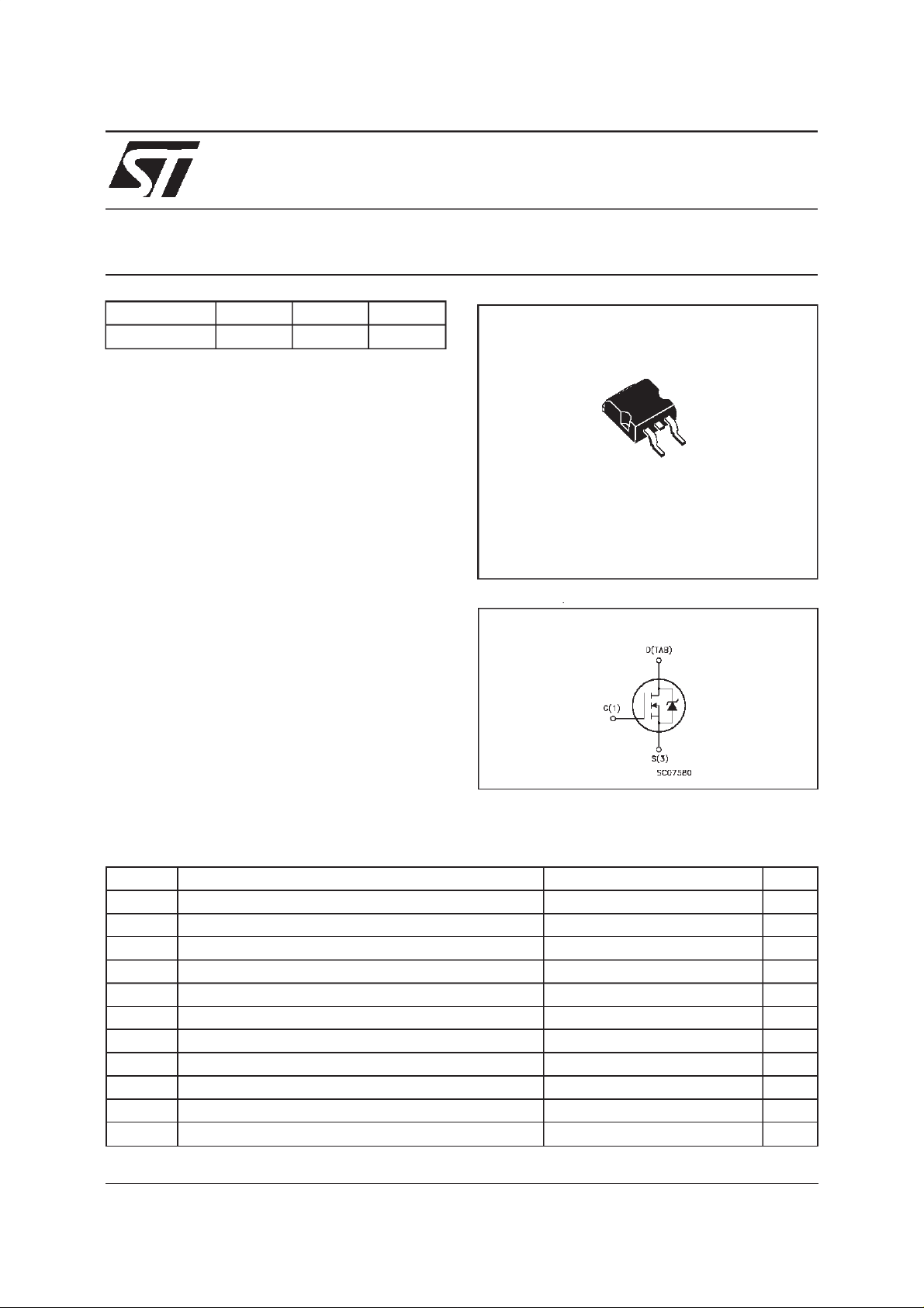
STripFET POWER MOSFET
3
1
D2PAK
TO-263
(suffix ”T4”)
INTERNAL SCHEMATIC DIAGRAM
ABSOLUTE MAXIMUM RATINGS
Symbol Parameter Value Unit
V
V
V
I
DM
P
dv/ dt Peak Diode Recovery voltage slope 7 V/ns
T
(•) Pulse width limited by safe operating area (1)ISD≤ 20 A, di/dt ≤ 300 A/µs, VDD≤ V
June 1999
Dra in- sour c e Volt age (VGS=0) 60 V
DS
Dra in- gat e Voltage (RGS=20kΩ)60V
DGR
Gat e-source Volt age
GS
I
Dra in Cu rr ent (contin uous ) a t Tc=25oC20A
D
I
Dra in Cu rr ent (contin uous ) a t Tc=100oC14A
D
20 V
±
(•) Drain Current (pulsed ) 80 A
Tot al Dissipation at Tc=25oC70W
tot
Der ati ng Fact or 0.47 W/
St orage Temperat ure -65 to 175
stg
T
Max. Operating Junct ion Temperat ure 175
j
(BR)DSS,Tj≤TJMAX
o
C
o
C
o
C
1/8
Page 2
STB20NE06L
THERMAL DATA
R
thj-case
Rthj-amb
R
thc-sink
T
AVALANCHE CHARACTERISTICS
Symbol Parameter Max Valu e Unit
I
AR
E
Ther mal Resistanc e Junct ion-case Max
Ther mal Resistanc e Junct ion-ambient Max
Ther mal Resistanc e C as e - sink Ty p
Maximum Lead T e m pe ra t ure For Soldering P urp os e
l
Avalanche Current, R epetitive or Not-Repetitive
(pulse width limited by T
Single Pul se Avalanc he Ener gy
AS
(starting T
=25oC, ID=IAR,VDD=35V)
j
max)
j
2.14
62.5
0.5
300
20 A
100 mJ
o
C/W
o
C/W
o
C/W
o
C
ELECTRICAL CHARACTERISTICS
=25oC unless otherwisespecified)
(T
case
OFF
Symbol Parameter Test Conditions Min. Typ. M ax. Unit
V
(BR)DSS
Drain-source
ID=250µAVGS=0 60 V
Break dow n Vo lt age
I
DSS
I
GSS
Zero Gate Volta ge
Drain Curre nt (V
GS
Gat e- bod y Leakag e
Current (V
DS
=0)
=0)
V
=MaxRating
DS
=MaxRating Tc= 125oC
V
DS
V
=± 20 V
GS
1
10
100 nA
±
ON(∗)
Symbol Parameter Test Conditions Min. Typ. M ax. Unit
V
GS(th)
R
DS(on)
I
D(on)
Gate Threshold Voltage VDS=VGSID= 250 µA11.72.0V
Sta t ic Drain-s our c e On
Resistance
VGS=5V ID=10A
=10V ID=10A
V
GS
On State Drain Current VDS>I
D(on)xRDS(on)max
0.07
0.06
20 A
0.085
0.07
VGS=10V
DYNAMIC
Symbol Parameter Test Conditions Min. Typ. M ax. Unit
g
(∗)Forward
fs
Tr ansc on duc tance
C
C
C
Input Capaci t ance
iss
Out put Capac itance
oss
Reverse Transfer
rss
Capacit a nc e
VDS>I
D(on)xRDS(on)maxID
=10 A 5 9 S
VDS=25V f=1MHz VGS= 0 800
125
40
µ
µA
Ω
Ω
pF
pF
pF
A
2/8
Page 3

STB20NE06L
ELECTRICAL CHARACTERISTICS
(continued)
SWITCHING ON
Symbol Parameter Test Conditions Min. Typ. M ax. Unit
t
d(on)
t
Tur n-on Delay T ime
Rise Time
r
VDD=30V ID=10A
R
=4.7 W VGS=5V
G
20
45
(see test circuit, figure 3)
Q
Q
Q
Tot al Gate Charge
g
Gat e- Source Charge
gs
Gate-Drain Charge
gd
VDD=48V ID=20A VGS=5V 14
8
4
20 nC
SWITCHING OFF
Symbol Parameter Test Conditions Min. Typ. M ax. Unit
t
r(Voff)
t
t
Off-voltage Rise T ime
Fall T ime
f
Cross-over Tim e
c
VDD=48V ID=20A
=4.7 Ω VGS=5V
R
G
(see test circuit, figure 5)
10
25
42
SOURCEDRAINDIODE
Symbol Parameter Test Conditions Min. Typ. M ax. Unit
I
SD
I
SDM
V
SD
t
Q
I
RRM
(∗) Pulsed:Pulse duration = 300µs, duty cycle 1.5%
(•) Pulse width limited by safe operating area
Source-drain Current
(•)
Source-drain Current
20
80
(pulsed)
(∗)ForwardOnVoltage ISD=20A VGS=0 1.5 V
Reverse Recovery
rr
Time
Reverse Recovery
rr
ISD= 20 A di/dt = 100 A/µs
=30V Tj= 150oC
V
DD
(see test circuit, figure 5)
65
130
Charge
Reverse Recovery
4
Current
ns
ns
nC
nC
ns
ns
ns
A
A
ns
nC
A
SafeOperating Area ThermalImpedance
3/8
Page 4

STB20NE06L
OutputCharacteristics
Transconductance
TransferCharacteristics
Static Drain-sourceOn Resistance
Gate Charge vs Gate-sourceVoltage
4/8
CapacitanceVariations
Page 5

STB20NE06L
NormalizedGate ThresholdVoltage vs
Temperature
Source-drainDiode ForwardCharacteristics
NormalizedOn Resistancevs Temperature
5/8
Page 6
STB20NE06L
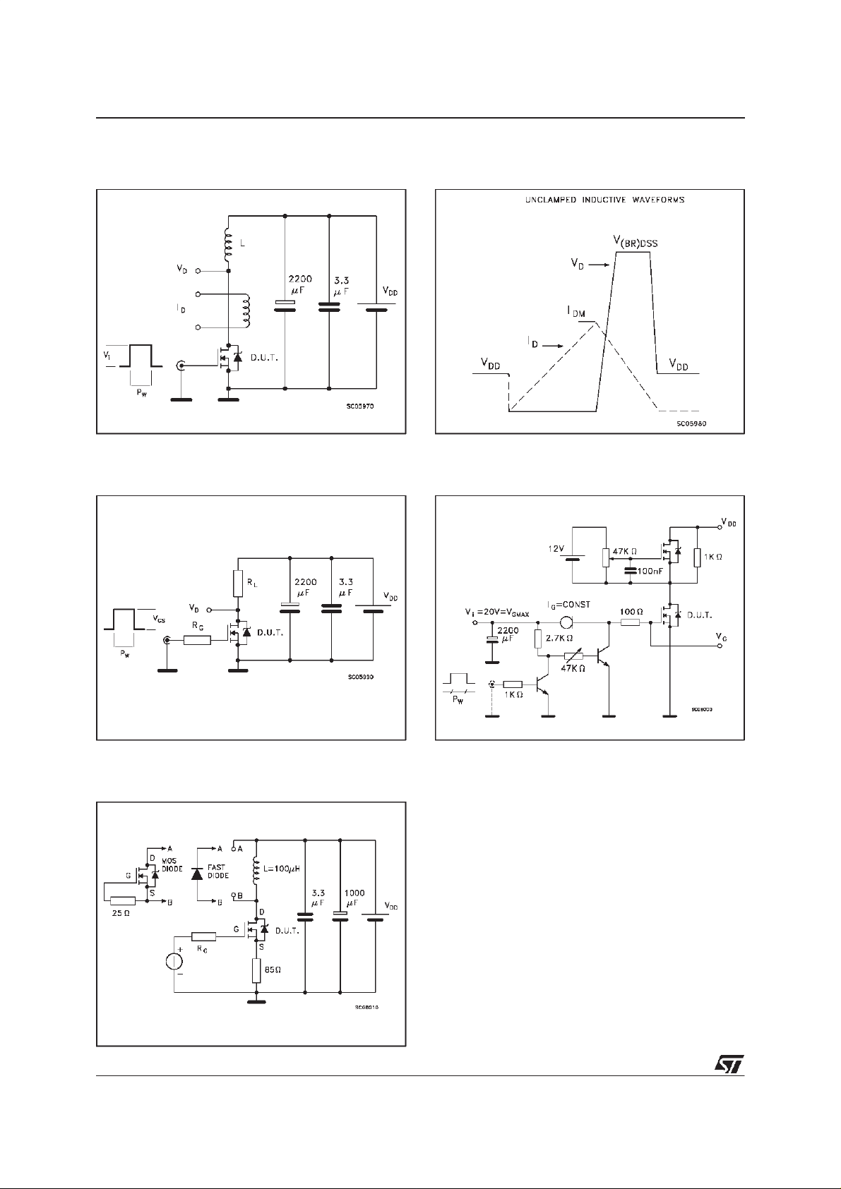
Fig. 1:
UnclampedInductiveLoad TestCircuit
Fig. 3: SwitchingTimes Test Circuits For
ResistiveLoad
Fig. 2:
UnclampedInductive Waveform
Fig. 4: Gate Chargetest Circuit
Fig. 5:
Test Circuit For InductiveLoad Switching
And Diode Recovery Times
6/8
Page 7

TO-263 (D2PAK) MECHANICAL DATA
STB20NE06L
DIM.
MIN. TYP. MAX. MIN. TYP. MAX.
A 4.4 4.6 0.173 0.181
A1 2.49 2.69 0.098 0.106
B 0.7 0.93 0.027 0.036
B2 1.14 1.7 0.044 0.067
C 0.45 0.6 0.017 0.023
C2 1.21 1.36 0.047 0.053
D 8.95 9.35 0.352 0.368
E 10 10.4 0.393 0.409
G 4.88 5.28 0.192 0.208
L 15 15.85 0.590 0.624
L2 1.27 1.4 0.050 0.055
L3 1.4 1.75 0.055 0.068
mm inch
D
A
C2
DETAIL”A”
C
A2
DETAIL”A”
A1
B2
E
L2
L
L3
B
G
P011P6/E
7/8
Page 8

STB20NE06L
Information furnishedis believedto be accurateand reliable.However, STMicroelectronics assumes no responsibility for the consequences
of use of such information nor for any infringement of patents or other rights of third parties which may result from its use. No license is
granted by implication or otherwise under any patent or patent rights of STMicroelectronics. Specificationmentioned in this publication are
subjectto change without notice.Thispublicationsupersedes and replacesall information previouslysupplied. STMicroelectronicsproducts
are not authorized for use as critical components in life support devicesor systemswithout express written approval of STMicroelectronics.
The STlogo is a trademark of STMicroelectronics
1999 STMicroelectronics – Printed in Italy – All Rights Reserved
STMicroelectronics GROUP OF COMPANIES
Australia - Brazil - China - Finland - France - Germany - Hong Kong - India - Italy - Japan - Malaysia - Malta - Morocco -
8/8
Singapore - Spain - Sweden - Switzerland - United Kingdom - U.S.A.
http://www.st.com
.
 Loading...