

Page 1
查询STB200NF04供应商
N-CHANNEL 40V - 120 A - 3.3 mΩ TO-220/D²PAK/I²PAK
STP200NF04
STB200NF04 - STB200NF04-1
STripFET™II MOSFET
Table 1: Ge neral Features
Type V
STB200NF04
STB200NF04-1
STP200NF04
■ STANDARD THRESHOLD DRIVE
■ 100% AVALANCHE TESTED
DSS
40 V
40 V
40 V
R
DS(on)
< 0.0037 Ω
< 0.0037 Ω
< 0.0037 Ω
I
D
120 A
120 A
120 A
Pw
310 W
310 W
310 W
DESCRIPTION
This MOSFET is th e latest developm ent of STM icroelectronics unique “Single Feature Size™”
strip-based process. The resulting transistor
shows extremely high pac king density for low onresistance, rugged avalance characteristics and
less critical alignment steps therefore a remarkable manufacturing reproducibility.
APPLICATIONS
■ HIGH CURRENT, HIGH SWI TCHIN G SPEED
■ AUTOMOTIVE
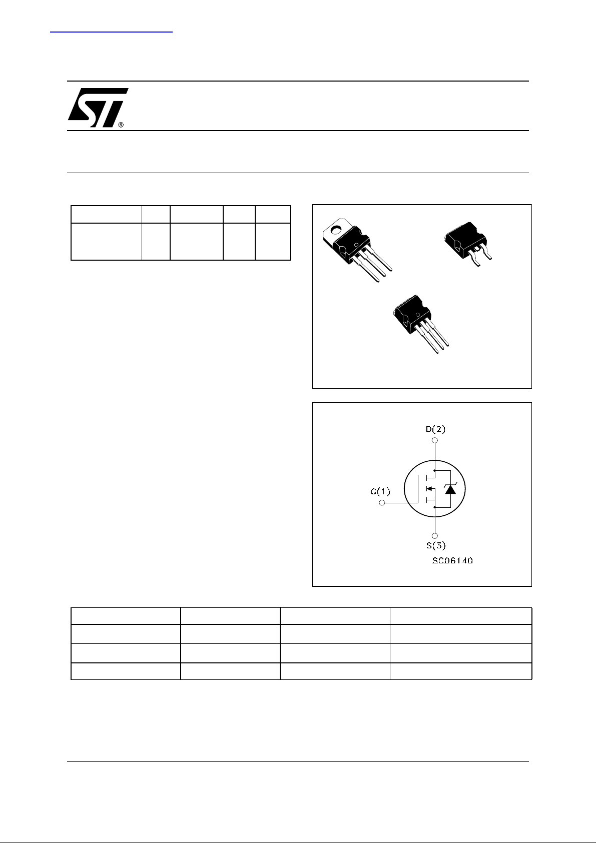
Figure 1: Package
3
2
1
1
D2PAK
TO-220
3
2
1
I2PAK
Figure 2: Internal Schematic Diagram
3
Table 2: Order Codes
SALES TYPE MARKING PACKAGE PACKAGING
STB200NF04T4 B200NF04
STB200NF04-1 B200NF04
STP200NF04 P200NF04 TO-220 TUBE
D
2
I
2
PAK
PAK
TAPE & REEL
TUBE
Rev. 3
1/15October 2004
Page 2
STP200NF04 - STB200NF04 - STB200NF04-1
Table 3: Absolute Maximum ratings
Symbol Parameter Value Unit
V
DS
V
DGR
V
GS
I
(#) Drain Current (continuos) at TC = 25°C
D
ID (#) Drain Current (continuos) at TC = 100°C
I
DM
P
TOT
dv/dt (1) Peak Diode Recovery voltage slope 1.5 V/ns
E
AS
T
j
T
stg
() Pulse wi dt h l i m i ted by safe operating area
≤120A, di/dt ≤500A/µs, VDD ≤ V
(1) I
SD
(2) Starting Tj = 25°C, Id = 60A, VDD=30 V
(#) Current Limited by Package
Table 4: Thermal Data
Rthj-case Thermal Resistance Junction-case Max 0.48 °C/W
Rthj-pcb Thermal Resistance Junction-pcb Max (see Figure 17) °C/W
Rthj-amb Thermal Resistance Junction-ambient (Free air) Max 62.5 °C/W
T
l
Drain-source Voltage (VGS = 0)
Drain-gate Voltage (RGS = 20 kΩ)
40 V
40 V
Gate- source Voltage ± 20 V
120 A
120 A
()
Drain Current (pulsed) 480 A
Total Dissipation at TC = 25°C
310 W
Derating Factor 2.07 W/°C
(2)
Single Pulse Avalanche Energy 1.3 J
Operating Junction Temperature
Storage Temperature
, Tj ≤ T
(BR)DSS
JMAX.
Maximum Lead Temperature For Soldering Purpose
-55 to 175 °C
2
TO-220 / I
PAK / D2PAK
300 °C
ELECTRICAL CHARACTERISTICS (T
=25°C UNLESS OTHERWISE SPECIFIED)
CASE
Table 5: On/Off
Symbol Parameter Test Conditions Min. Typ. Max. Unit
V
(BR)DSS
I
DSS
I
GSS
V
GS(th)
R
DS(on)
Drain-source
Breakdown Voltage
Zero Gate Voltage
Drain Current (V
GS
= 0)
Gate-body Leaka ge
Current (V
DS
= 0)
Gate Threshold Voltage
Static Drain-source On
Resistance
ID = 250 µA, VGS = 0 40 V
V
= Max Rating
DS
= Max Rating, TC = 125 °C
V
DS
V
= ± 20V ±100 nA
GS
V
= VGS, ID = 250µA
DS
24V
1
10
VGS = 10V, ID = 90 A 3.3 3.7 mΩ
µA
µA
2/15
Page 3
STP200NF04 - STB200NF04 - STB200NF04-1
ELECTRICAL CHARACTERISTICS (CONTINUED)
Table 6: Dynamic
Symbol Parameter Test Conditions Min. Typ. Max. Unit
(1) Forward Transconductance VDS = 15 V, ID= 90 A 150 S
g
fs
C
iss
C
oss
C
rss
Table 7: Switching On/Off
Symbol Parameter Test Conditions Min. Typ. Max. Unit
t
d(on)
t
r
t
d(off)
t
f
Q
g
Q
gs
Q
gd
Input Capacitance
Output Capacitance
Reverse Transfer
Capacitance
Turn-on Delay Time
Rise Time
Turn-off Delay Time
Fall Time
Total Gate Charge
Gate-Source Charge
Gate-Drain Charge
= 25V, f = 1 MHz, VGS = 0 5100
V
DS
= 20 V, ID = 90 A
V
DD
R
=4.7Ω VGS = 10 V
G
(see Figure 20)
= 20V, ID = 120 A,
V
DD
V
= 10V
GS
(see Figure 23)
1600
600
30
320
140
120
170
30
62
210
pF
pF
pF
ns
ns
ns
ns
nC
nC
nC
Table 8: Source Drain Diode
Symbol Parameter Test Conditions Min. Typ. Max. Unit
I
SD
I
SDM
VSD (1)
t
rr
Q
rr
I
RRM
(1) Pulsed: Pulse duratio n = 300 µs, duty cycl e 1.5 %.
(2) Pulse wi dt h l i m i ted by safe operat i ng area.
(2)
Source-drain Current
Source-drain Current (pulsed)
Forward On Voltage
Reverse Recovery Time
Reverse Recovery Charge
Reverse Recovery Current
ISD = 120 A, VGS = 0
= 120 A, di/dt = 100A/µs
I
SD
V
= 30V, Tj = 150°C
DD
(see Figure 21)
85
190
4.5
120
480
1.3 V
A
A
ns
nC
A
3/15
Page 4
STP200NF04 - STB200NF04 - STB200NF04-1
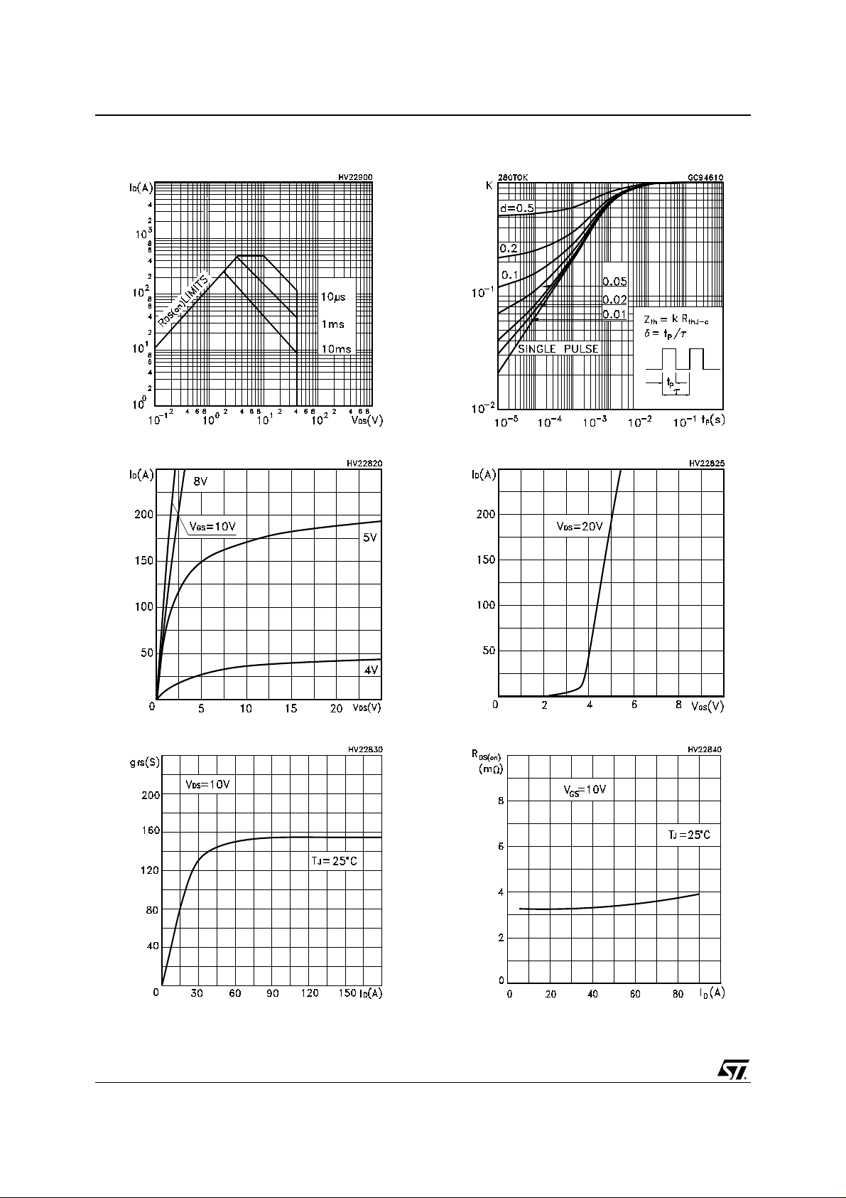
Figure 3: Safe Operating Area
Figure 4: Output Characteristics
Figure 6: Thermal Impedance
Figure 7: Transfer Characteristics
Figure 5: Transconductance
4/15
Figure 8: Static Drain-source On Resistance
Page 5
STP200NF04 - STB200NF04 - STB200NF04-1
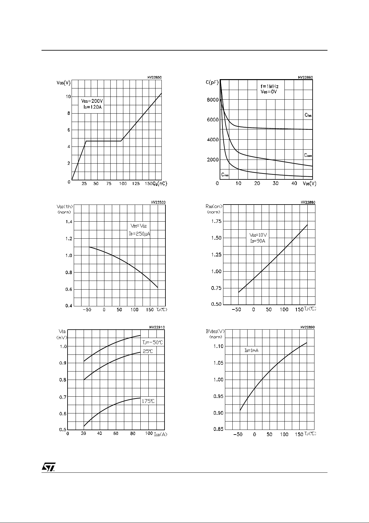
Figure 9: Gate Charge vs Gate-source Voltag e
Figure 10: Normalized Gate Thereshold Voltage vs Temperature
Figure 12: Capacitance Variations
Figure 13: Normal ized On R esistance vs Temperature
Figure 11: Dource -Drain Diode Forward Ch aracteristics
Figure 14: Normalized Breakdown Voltage vs
Temperature
5/15
Page 6

STP200NF04 - STB200NF04 - STB200NF04-1
Figure 15: Thermal Resistance Rthj-a vs PCB
Copper Area
Figure 16: Max Power Dissipation vs PCB Copper Area
6/15
Page 7

STP200NF04 - STB200NF04 - STB200NF04-1
Figure 17: Allowable lav vs. Time in Avalanche
The previous curve gives the safe operating area for unclamped inductive loads, single pulse or repetitive,
under the following conditions:
P
D(AVE)
E
AS(AR)
= 0.5 * (1.3 * BV
= P
D(AVE)
* t
AV
DSS
* IAV)
Where:
is the Allowable Current in Avalanche
I
AV
P
t
AV
is the Average Power Dissipation in Avalanche (Single Pulse)
D(AVE)
is the Time in Avalanche
To derate above 25 °C, at fixed I
I
AV
Where:
= K * R
Z
th
is the value coming from Normalized Thermal Response at fixed pulse width equal to TAV.
th
the following equation must be applied:
AV,
= 2 * (T
jmax
- T
) / (1.3 * BV
CASE
DSS
* Zth)
7/15
Page 8

STP200NF04 - STB200NF04 - STB200NF04-1
SPICE THERMAL MODEL
Table 9: 6th Order RC Network
Parameter Node Value
CTHERM1 1 - 2 1.4958E-3
CTHERM2 2 - 3 3.5074E-2
CTHERM3 3 - 4 5.939E-2
CTHERM4 4 - 5 9.7411E-2
CTHERM5 5 - 6 8.8596E-2
CTHERM6 6 - 7 8.2755E-1
RTHERM1 1 - 2 0.0384
RTHERM2 2 - 3 0.0624
RTHERM3 3 - 4 0.072
RTHERM4 4 - 5 0.0912
RTHERM5 5 - 6 0.1008
RTHERM6 6 - 7 0.1152
Figure 18 : Sc hematic of 6th Order R C N et wor k
8/15
Page 9

STP200NF04 - STB200NF04 - STB200NF04-1
Figure 19: Unclamped Inductive Load Test Circuit
Figure 20: Switching Times Test Circuit For
Resistive Load
Figure 22: Unclamped Inductive Wafeform
Figure 23: Gate Charge Test Circuit
Figure 21: Test Circuit For Inductive Load
Switching and Diode Recovery Times
9/15
Page 10

STP200NF04 - STB200NF04 - STB200NF04-1
TO-220 MECHANICAL DATA
DIM.
A 4.40 4.60 0.173 0.181
b 0.61 0.88 0.024 0.034
b1 1.15 1.70 0.045 0.066
c 0.49 0.70 0.019 0.027
D 15.25 15.75 0.60 0.620
E 10 10.40 0.393 0.409
e 2.40 2.70 0.094 0.106
e1 4.95 5.15 0.194 0.202
F 1.23 1.32 0.048 0.052
H1 6.20 6.60 0.244 0.256
J1 2.40 2.72 0.094 0.107
L 13 14 0.511 0.551
L1 3.50 3.93 0.137 0.154
L20 16.40 0.645
L30 28.90 1.137
øP
Q 2.65 2.95 0.104 0.116
MIN. TYP MAX. MIN. TYP. MAX.
3.75 3.85 0.147 0.151
mm. inch
10/15
Page 11

STP200NF04 - STB200NF04 - STB200NF04-1
D2PAK MECHANICAL DATA
TO-247 MECHANICAL DATA
DIM.
A 4.4 4.6 0.173 0.181
A1 2.49 2.69 0.098 0.106
A2 0.03 0.23 0.001 0.009
B 0.7 0.93 0.027 0.036
B2 1.14 1.7 0.044 0.067
C 0.45 0.6 0.017 0.023
C2 1.23 1.36 0.048 0.053
D 8.95 9.35 0.352 0.368
D1 8 0.315
E 10 10.4 0.393
E1 8.5 0.334
G 4.88 5.28 0.192 0.208
L 15 15.85 0.590 0.625
L2 1.27 1.4 0.050 0.055
L3 1.4 1.75 0.055 0.068
M 2.4 3.2 0.094 0.126
R0.4 0.015
V2 0º 4º
MIN. TYP MAX. MIN. TYP. MAX.
mm. inch
3
1
11/15
Page 12

STP200NF04 - STB200NF04 - STB200NF04-1
TO-262 (I2PAK) MECHANICAL DATA
DIM.
A 4.40 4.60 0.173 0.181
A1 2.40 2.72 0.094 0.107
b 0.61 0.88 0.024 0.034
b1 1.14 1.70 0.044 0.066
c 0.49 0.70 0.019 0.027
c2 1.23 1.32 0.048 0.052
D 8.95 9.35 0.352 0.368
e 2.40 2.70 0.094 0.106
e1 4.95 5.15 0.194 0.202
E 10 10.40 0.393 0.410
L 13 14 0.511 0.551
L1 3.50 3.93 0.137 0.154
L2 1.27 1.40 0.050 0.055
MIN. TYP MAX. MIN. TYP. MAX.
mm. inch
12/15
Page 13

STP200NF04 - STB200NF04 - STB200NF04-1
D2PAK FOOTPRINT
TAPE AND REEL SHIPMENT (suffix ”T4”)*
TUBE SHIPMENT (no suffix)*
REEL MECHANICAL DATA
DIM.
A 330 12.992
B 1.5 0.059
C 12.8 13.2 0.504 0.520
D 20.2 0795
G 24.4 26.4 0.960 1.039
N 100 3.937
T 30.4 1.197
mm inch
MIN. MAX. MIN. MAX.
T APE MECHANICAL DATA
DIM.
A0 10.5 10.7 0.413 0.421
B0 15.7 15.9 0.618 0.626
D 1.5 1.6 0.059 0.063
D1 1.59 1.61 0.062 0.063
E 1.65 1.85 0.065 0.073
F 11.4 11.6 0.449 0.456
K0 4.8 5.0 0.189 0.197
P0 3.9 4.1 0.153 0.161
P1 11.9 12.1 0.468 0.476
P2 1.9 2.1 0.075 0.082
R 50 1.574
T 0.25 0.35 0.0098 0.0137
W 23.7 24.3 0.933 0.956
* on sales type
mm inch
MIN. MAX. MIN. MAX.
BASE QTY BULK QTY
1000 1000
13/15
Page 14

STP200NF04 - STB200NF04 - STB200NF04-1
Table 10: Revision History
Date Revision Description of Change s
28-Sep-2004 2 New Stylesheet. No Content Change
11-Oct-2004 3 Final datasheet
14/15
Page 15

STP200NF04 - STB200NF04 - STB200NF04-1
Information furnished is believed to be accurate and reliable. However, STMicroelectronics assumes no responsibility for the consequences
of use of s uch inf ormati on nor for a ny infr ing eme nt o f p atent s or o ther ri ghts of third parti es wh ic h m ay r esul t fr om its us e. No lic ens e is gr an ted
by implication or otherwise under any patent or patent rights of STMicroelectronics. Specifications mentioned in this publication are subject
to change without notice. This publication supersedes and replaces all information previously supplied. STMicroelectronics products are not
authorized for use as critical components in life support devices or systems without express written approval of STMicroelectronics.
The ST logo is a registered trademark of STMicroelectronics
All other names are the property of their respective owners
© 2004 STMicroelectronics - All Rights Reserved
STMicroelectronics group of companies
Australia - Belgium - Brazil - Canada - China - Czech Republic - Finland - France - Germany - Hong Kong - India - Israel - Italy - Japan -
Malaysia - Malta - Morocco - Singapore - Spain - Sweden - Switzerland - United Kingdom - United States of America
15/15
 Loading...