

Page 1
STB19NB20
N - CHANNEL ENHANCEMENT MODE
PowerMESH MOSFET
TYPE V
DSS
R
DS(on)
I
D
ST B19NB20 200 V < 0.180 Ω 19 A
■ TYPICALR
■ EXTREMELYHIGH dv/dtCAPABILITY
■ 100%AVALANCHETESTED
■ VERYLOW INTRINSIC CAPACITANCES
■ GATECHARGE MINIMIZED
■ FORTHROUGH-HOLE VERSION CONTACT
DS(on)
= 0.150 Ω
SALESOFFICE
DESCRIPTION
Usingthe latesthigh voltageMESHOVERLAY
process, STMicroelectronics has designed an
advanced family of Power MOSFETs with
outstanding performance. The new patent
pending strip layout coupled with the Company’s
proprietary edge termination structure, gives the
lowest RDS(on) per area, exceptional avalanche
and dv/dt capabilities and unrivalled gate charge
and switching characteristics.
APPLICATIONS
■ HIGHCURRENT, HIGH SPEED SWITCHING
■ SWITCHMODE POWER SUPPLIES (SMPS)
■ DC-AC CONVERTERS FOR WELDING
EQUIPMENTANDUNINTERRUPTIBLE
POWERSUPPLIESAND MOTOR DRIVE
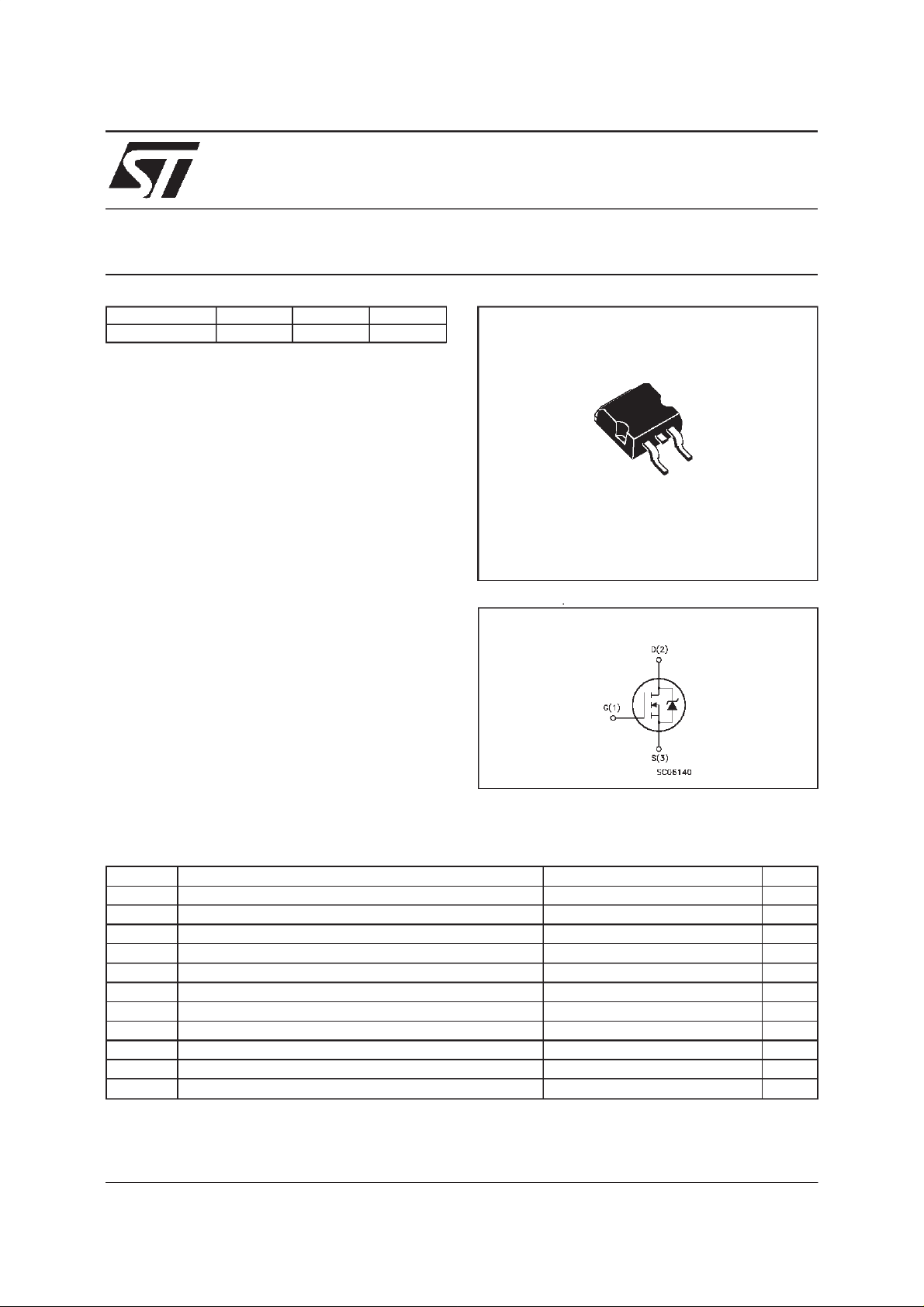
3
1
D2PAK
TO-263
(suffix ”T4”)
INTERNAL SCHEMATIC DIAGRAM
ABSOLUTE MAXIMUM RATINGS
Symb o l Parameter Val u e Uni t
V
V
V
I
DM
P
dv/dt(
T
(•) Pulse width limited by safe operating area (1)ISD≤ 19A, di/dt ≤ 300A/µs, VDD≤ V
June 1998
Drain-sourc e Voltage (VGS=0) 200 V
DS
Drain- ga t e Voltage (RGS=20kΩ)200V
DGR
Gate-s ource Volt age
GS
I
Drain Cur rent ( cont i nuous) at Tc=25oC19A
D
I
Drain Cur rent ( cont i nuous) at Tc= 100oC12A
D
30 V
±
(•) Drain Current (pulsed) 76 A
Total Dissipation at Tc=25oC125W
tot
Derating Factor 1 W/
1) Peak D iode R ecov e r y voltage slope 5.5 V/ ns
St orage Temper at u re -65 to 150
stg
T
Max. Operating Junction Temp erat u re 150
j
(BR)DSS
,Tj≤T
JMAX
o
C
o
C
o
C
1/8
Page 2
STB19NB20
THERMAL DATA
R
thj-case
R
thj-amb
R
thc-sink
T
AVALANCHE CHARACTERISTICS
Symbol Parameter Max V alue Unit
I
AR
E
Ther mal Res istance Junct ion-case Max 1
Ther mal Res istance Junct ion-ambie nt Max
Ther mal Res istance C as e - sink Ty p
Maximum Lead T e m pe rat ur e F or So ldering Purpose
l
Avalanche Current, Repetitive or Not-Repetitive
(pulse width limited by T
Single Pul se Avalanc he E nergy
AS
(starting T
=25oC, ID=IAR,VDD=50V)
j
max)
j
62.5
0.5
300
19 A
580 mJ
o
C/W
o
C/W
o
C/W
o
C
ELECTRICAL CHARACTERISTICS
=25oC unless otherwisespecified)
(T
case
OFF
Symbol Parameter Test Conditions Min. Typ. Max. Unit
V
(BR)DSS
Drain-source
ID=250µAVGS= 0 200 V
Break dow n Vo lt age
I
DSS
I
GSS
Zero Gate Voltage
Drain Curre nt (V
GS
Gat e- bod y Leakag e
Current (V
DS
=0)
=0)
V
=MaxRating
DS
=MaxRating Tc=125oC
V
DS
V
= ± 30 V ± 100 nA
GS
1
10
ON(∗)
Symbol Parameter Test Conditions Min. Typ. Max. Unit
V
GS(th)
R
DS(on)
Gate Threshold Voltage VDS=VGSID= 250 µ A 345V
Sta t ic Drain-s our c e On
VGS=10V ID= 9.5 A 0.150 0. 180
Resistance
I
D(on)
On StateDrain Current VDS>I
D(on)xRDS(on)ma x
19 A
VGS=10V
DYNAMIC
Symbol Parameter Test Conditions Min. Typ. Max. Unit
g
(∗)Forward
fs
Tr ansc on duc tance
C
C
C
Input Capaci t ance
iss
Out put Capac itance
oss
Reverse Transfer
rss
Capacit a nc e
VDS>I
D(on)xRDS(on)ma xID
=9.5 A 3 S
VDS=25V f=1MHz VGS= 0 1000
285
45
1350
385
60
µ
µA
Ω
pF
pF
pF
A
2/8
Page 3
STB19NB20
ELECTRICAL CHARACTERISTICS
(continued)
SWITCHINGON
Symbol Parameter Test Conditions Min. Typ. Max. Unit
t
d(on)
t
r
Turn-on Time
Rise Time
VDD=100V ID= 9.5 A
R
=4.7
G
Ω
VGS=10V
15
15
20
20
(see test circuit, figure 3)
Q
Q
Q
Tot al Gate C harge
g
Gat e- Source Charge
gs
Gate-Drain Charge
gd
VDD= 160 V ID=19A VGS=10V 29
9.5
13
40 nC
SWITCHINGOFF
Symbol Parameter Test Conditions Min. Typ. Max. Unit
t
r(Voff)
t
t
Off-voltage Ris e Time
Fall T ime
f
Cross-over Time
c
VDD=160V ID=19A
=4.7 Ω VGS=10V
R
G
(see test circuit, figure 5)
10
10
20
15
15
30
SOURCEDRAINDIODE
Symbol Parameter Test Conditions Min. Typ. Max. Unit
I
SD
I
SDM
V
SD
t
Q
I
RRM
(∗) Pulsed:Pulse duration = 300µs, duty cycle 1.5%
(•) Pulse width limited by safeoperating area
Source-drain Current
(•)
Source-drain Current
19
76
(pulsed)
(∗)ForwardOnVoltage ISD=19 A VGS=0 1.5 V
Reverse Recovery
rr
Time
Reverse Recovery
rr
ISD=19 A di/dt = 10 0 A/µs
=50V Tj= 150oC
V
DD
(see test circuit, figure 5)
210
1.5
Charge
Reverse Recovery
14.5
Current
ns
ns
nC
nC
ns
ns
ns
A
A
ns
µ
A
C
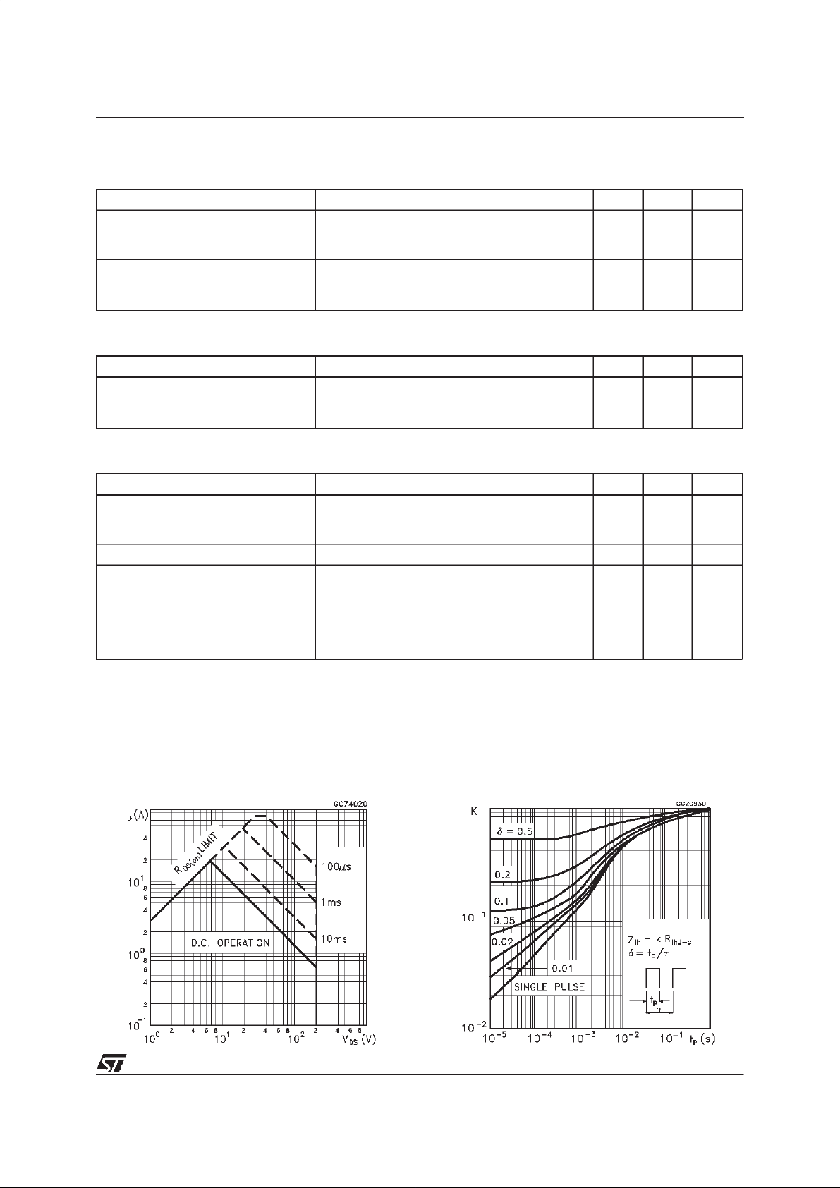
SafeOperating Area ThermalImpedance
3/8
Page 4

STB19NB20
OutputCharacteristics
Transconductance
TransferCharacteristics
Static Drain-sourceOn Resistance
Gate Charge vs Gate-sourceVoltage
4/8
CapacitanceVariations
Page 5

STB19NB20
NormalizedGate ThresholdVoltage vs
Temperature
Source-drainDiode ForwardCharacteristics
NormalizedOn Resistancevs Temperature
5/8
Page 6

STB19NB20
Fig. 1:
UnclampedInductiveLoad Test Circuit
Fig. 3: SwitchingTimes Test CircuitsFor
ResistiveLoad
Fig. 2:
UnclampedInductive Waveform
Fig. 4: Gate Charge test Circuit
Fig. 5:
Test CircuitFor InductiveLoad Switching
And Diode Recovery Times
6/8
Page 7

TO-263 (D2PAK) MECHANICAL DATA
STB19NB20
DIM.
MIN. TYP. MAX. MIN. TYP. MAX.
A 4.4 4.6 0.173 0.181
A1 2.49 2.69 0.098 0.106
B 0.7 0.93 0.027 0.036
B2 1.14 1.7 0.044 0.067
C 0.45 0.6 0.017 0.023
C2 1.21 1.36 0.047 0.053
D 8.95 9.35 0.352 0.368
E 10 10.4 0.393 0.409
G 4.88 5.28 0.192 0.208
L 15 15.85 0.590 0.624
L2 1.27 1.4 0.050 0.055
L3 1.4 1.75 0.055 0.068
mm inch
D
A
C2
DETAIL”A”
C
A2
DETAIL”A”
A1
B2
E
L2
L
L3
B
G
P011P6/E
7/8
Page 8

STB19NB20
Information furnished is believed tobeaccurateand reliable.However, STMicroelectronics assumes no responsibility for the consequences
of use of such information nor for any infringement of patents or other rights of third parties which may result from its use. No license is
granted by implication or otherwise under any patent or patent rights of STMicroelectronics. Specification mentioned in this publicationare
subjecttochange without notice.This publication supersedes andreplaces all information previouslysupplied.STMicroelectronics products
are not authorized for use as critical components in life support devices or systemswithout express written approval of STMicroelectronics.
The STlogo is a trademark ofSTMicroelectronics
1999 STMicroelectronics – Printed in Italy – All Rights Reserved
STMicroelectronics GROUP OF COMPANIES
Australia - Brazil - Canada - China - France - Germany - Italy - Japan- Korea - Malaysia - Malta - Mexico - Morocco - The Netherlands -
8/8
Singapore - Spain - Sweden - Switzerland - Taiwan- Thailand - UnitedKingdom - U.S.A.
http://www.st.com
.
 Loading...