

Page 1
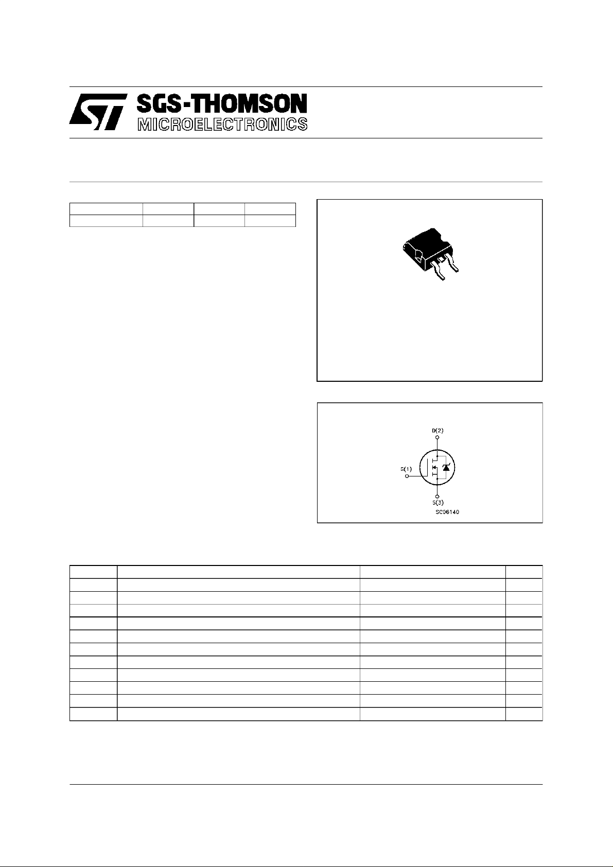
N - CHANNEL ENHANCEMENT MODE
TYPE V
DSS
R
DS(on)
ST B19NB20 200 V < 0.18 0 Ω 19 A
I
D
STB19NB20
PowerMESH MOSFET
PRELIMINARY DATA
■ TYPICALR
■ 100% AVALANCHETESTED
■ VERYLOW INTRINSICCAPACITANCES
■ GATECHARGEMINIMIZED
■ EXTREMELY HIGH dv/dt CAPABILITY
■ FOR THROUGH-HOLE VERSIONCONTACT
DS(on)
=0.150 Ω
SALESOFFICE
DESCRIPTION
Using the latest high voltage MESH
OVERLAY process, SGS-Thomson has
designed an advanced family of Power
MOSFETs with outstanding performance. The
new patent pending strip layout coupled with the
Company’s proprietary edge termination
structure, gives the lowest RDS(on) per area,
exceptional avalanche and dv/dt capabilitiesand
unrivalled gate charge and switching
characteristics.
APPLICATIONS
■ HIGH CURRENT, HIGHSPEEDSWITCHING
■ SWITCHMODEPOWER SUPPLIES(SMPS)
■ DC-ACCONVERTERS FOR WELDING
EQUIPMENTAND UNINTERRUPTIBLER E
3
1
D2PAK
TO-263
(Suffix ”T4”)
INTERNAL SCHEMATIC DIAGRAM
ABSOLUTE MAXIMUM RATINGS
Symbol Parameter Value Unit
V
V
DGR
V
I
DM
P
dv/dt(
T
(•) Pulse width limited by safe operatingarea (1)ISD≤ 19A, di/dt ≤ 200 A/µs,VDD≤ V
October 1997
This ispreliminary informationon a new product now in development or undergoing evaluation. Details are subject to changewithout notice.
Drain-source Voltage (VGS=0) 200 V
DS
Drain- gate Voltage (RGS=20kΩ)
Gate-s ource Voltage ± 30 V
GS
I
Drain Curr ent ( continuous ) at Tc=25oC19A
D
I
Drain Curr ent ( continuous ) at Tc=100oC12A
D
200 V
(•) Dra in Curr ent ( pulsed) 76 A
Total Dissipation at Tc=25oC125W
tot
Derat ing F actor 1 W /
1) Peak Diode Rec overy voltag e slope 5.5 V/ ns
Storage Temperature -65 to 1 50
stg
Max. Operating Junct i on Temperature 150
T
j
(BR)DSS
,Tj≤T
JMAX
o
C
o
C
o
C
1/6
Page 2
STB19NB20
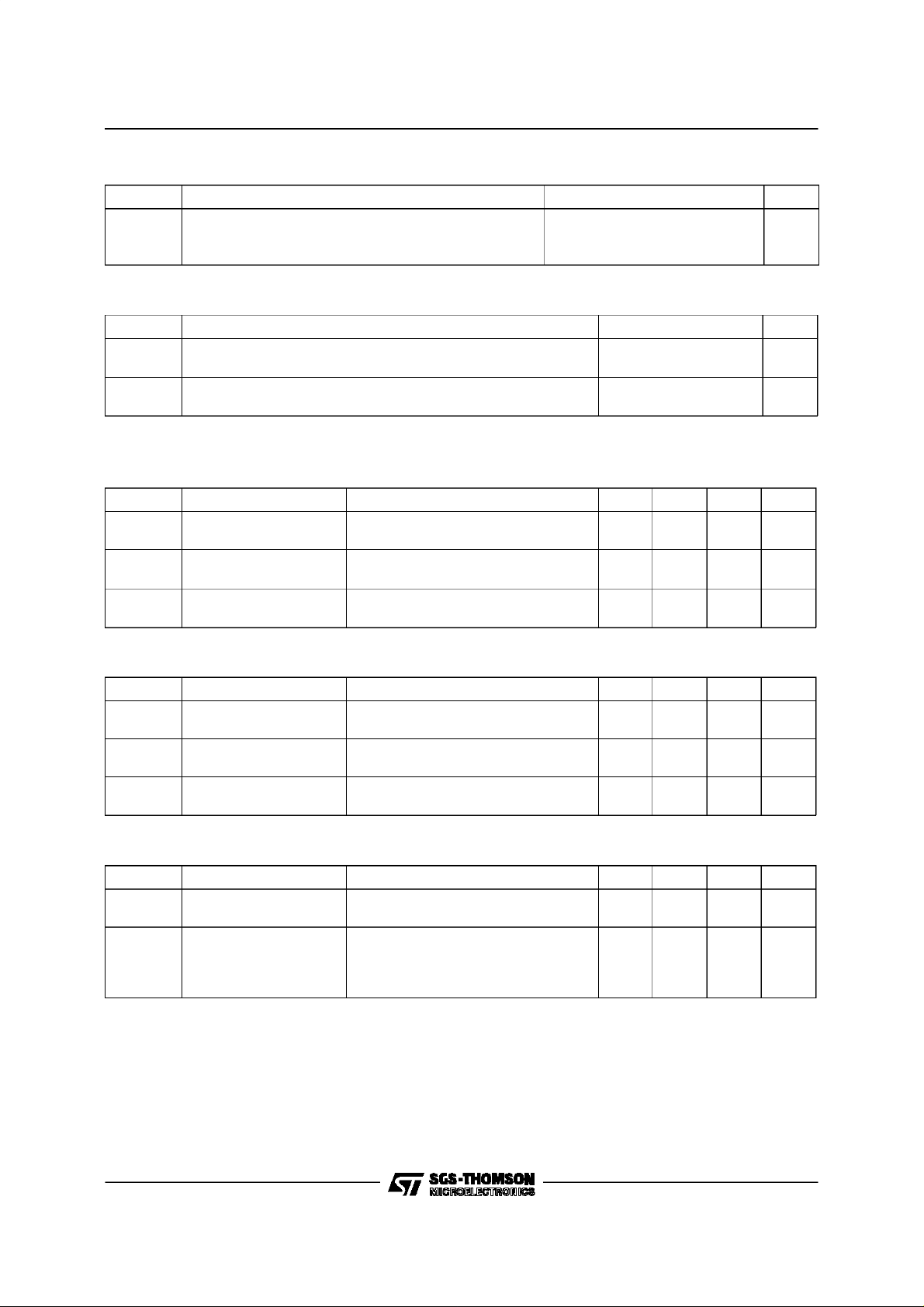
THERMAL DATA
R
thj-case
R
thj-amb
R
thc-sin k
T
AVALANCHE CHARACTERISTICS
Symbol Para met e r Max Value Uni t
I
AR
E
Ther mal Resistance Junction-case Max 1
Ther mal Resistance Junction-ambie nt Max
Ther mal Resistance Case-si nk T yp
Maximum Lead Tem perature For Soldering Purpose
l
Avalanche Curr e nt , Repetitiv e or Not-Re petitive
(pulse width li mited b y T
Single Pulse Avalanche Energy
AS
(starting T
=25oC, ID=IAR,VDD=50V)
j
max, δ <1%)
j
62.5
0.5
300
19 A
200 mJ
o
C/W
o
C/W
o
C/W
o
C
ELECTRICAL CHARACTERISTICS (T
=25oC unlessotherwise specified)
case
OFF
Symbol Parameter Test Conditions Min. Typ. Max. Unit
V
(BR)DSS
Drain-source
=250µAVGS=0
I
D
200 V
Breakdown Voltage
I
I
DSS
GSS
Zer o Gat e Voltage
Drain Current (V
GS
Gat e-body Leakage
Current (V
DS
=0)
=0)
V
=MaxRating
DS
=MaxRating Tc=125oC
V
DS
= ± 30 V
V
GS
1
10
± 100 nA
ON (∗)
Symbol Parameter Test Conditions Min. Typ. Max. Unit
V
GS(th )
Gate Threshold
V
DS=VGSID
=250µA
345V
Voltage
R
DS(on)
Stati c D rain-source O n
VGS=10V ID= 9.5 A 0.150 0.180 Ω
Resistance
I
D(on)
On State Drain Current VDS>I
D(on)xRDS(on)max
19 A
VGS=10V
DYNAMIC
Symbol Parameter Test Conditions Min. Typ. Max. Unit
g
(∗)Forward
fs
Tr ansconductance
C
C
C
Input Capac i t an c e
iss
Out put Capacitance
oss
Reverse Transf er
rss
Capa cit an c e
VDS>I
D(on)xRDS(on)maxID
=9.5 A 3 S
VDS=25V f=1MHz VGS= 0 1000
285
45
1350
385
60
µA
µA
pF
pF
pF
2/6
Page 3
STB19NB20
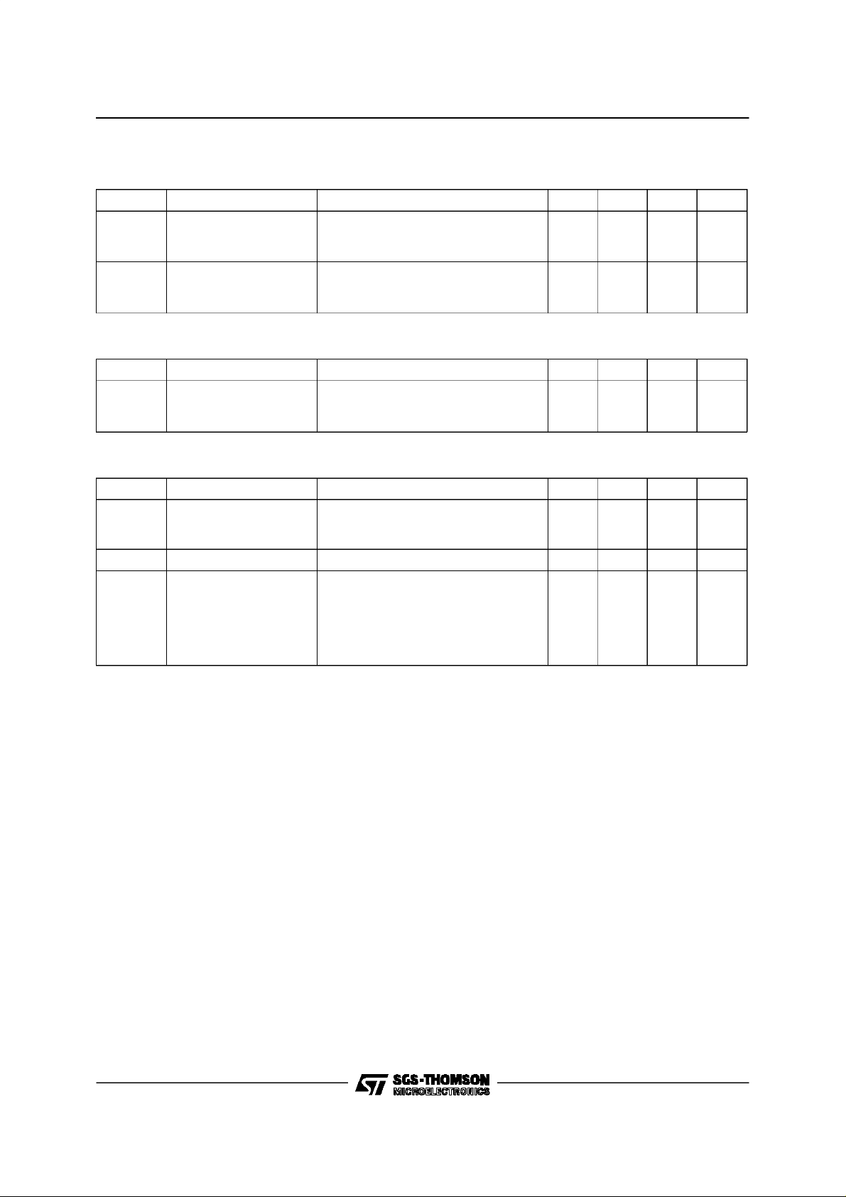
ELECTRICAL CHARACTERISTICS (continued)
SWITCHINGON
Symbol Parameter Test Conditions Min. Typ. Max. Unit
t
d(on)
t
r
Turn-on Time
Rise Time
VDD=100V ID=9.5A
=4.7 Ω VGS=10V
R
G
15
15
(see test circuit, figure 3)
Q
Q
Q
Total Gate Charge
g
Gat e-Source Cha rge
gs
Gate-Drain Charge
gd
VDD=160V ID=19A VGS=10V 29
9.5
13
SWITCHINGOFF
Symbol Parameter Test Conditions Min. Typ. Max. Unit
t
r(Voff)
t
t
Of f - voltage Rise Time
Fall Time
f
Cross-over T im e
c
VDD=160V ID=19A
=4.7 Ω VGS=10V
R
G
(see test circuit, figure 5)
10
10
20
SOURCE DRAIN DIODE
Symbol Parameter Test Conditions Min. Typ. Max. Unit
I
SD
I
SDM
V
SD
t
Q
I
RRM
(∗) Pulsed: Pulse duration =300 µs,duty cycle 1.5 %
(•) Pulse width limited by safe operating area
Source-drain Curre nt
(•)
Source-drain Curre nt
(pulsed)
(∗) F orward On Voltage ISD=19 A VGS=0 1.5 V
Reverse Recov ery
rr
Time
Reverse Recov ery
rr
=19 A di/dt = 100 A/µs
I
SD
=50V Tj=150oC
V
DD
(see test circuit, figure 5)
210
1.5
Charge
Reverse Recov ery
14.5
Current
20
20
40 nC
15
15
30
19
76
ns
ns
nC
nC
ns
ns
ns
A
A
ns
µC
A
3/6
Page 4
STB19NB20
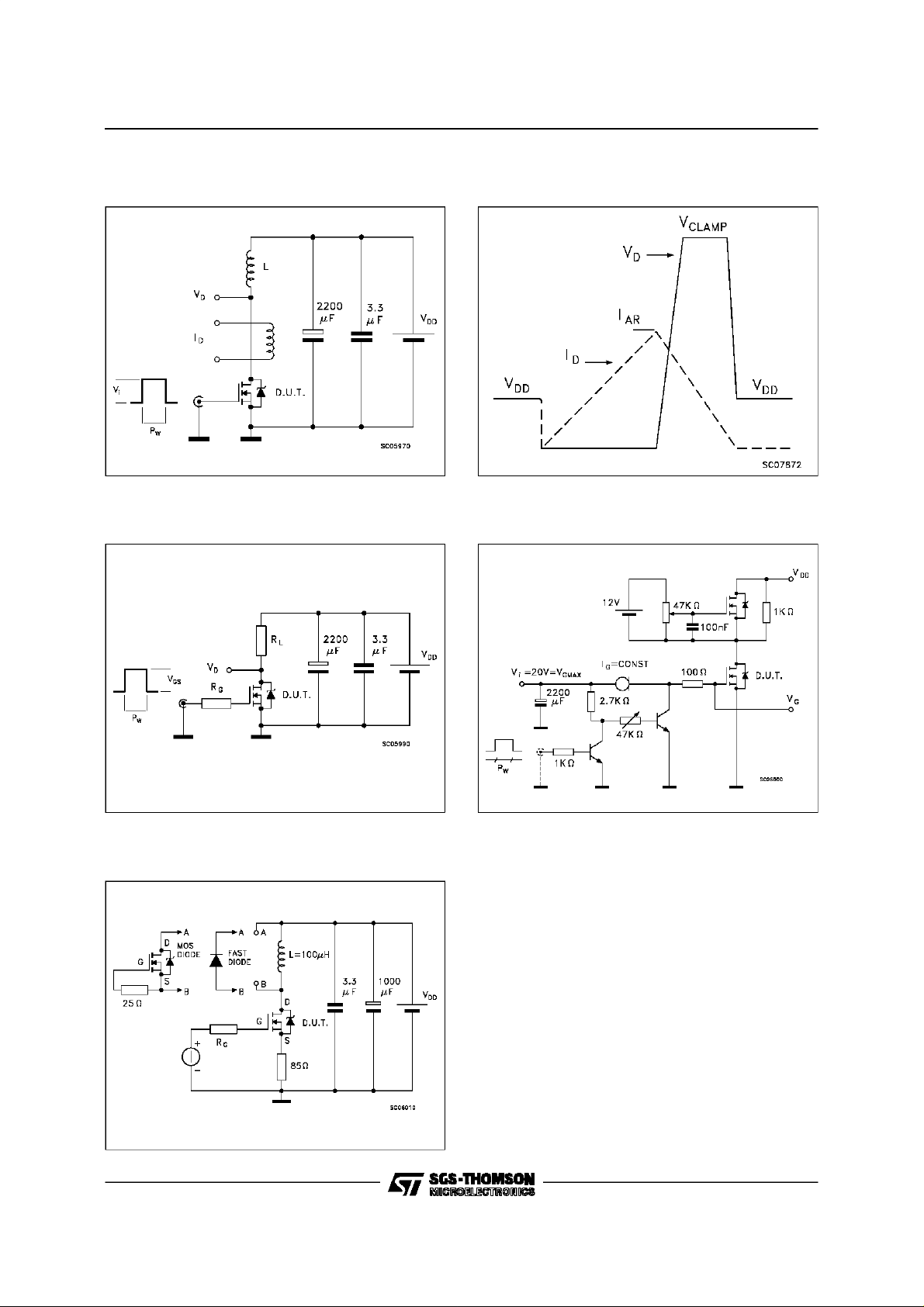
Fig. 1: Unclamped InductiveLoad Test Circuit
Fig. 3: SwitchingTimesTest CircuitsFor
ResistiveLoad
Fig. 2: Unclamped Inductive Waveform
Fig. 4: Gate Charge test Circuit
Fig. 5: Test Circuit For Inductive Load Switching
And Diode RecoveryTimes
4/6
Page 5
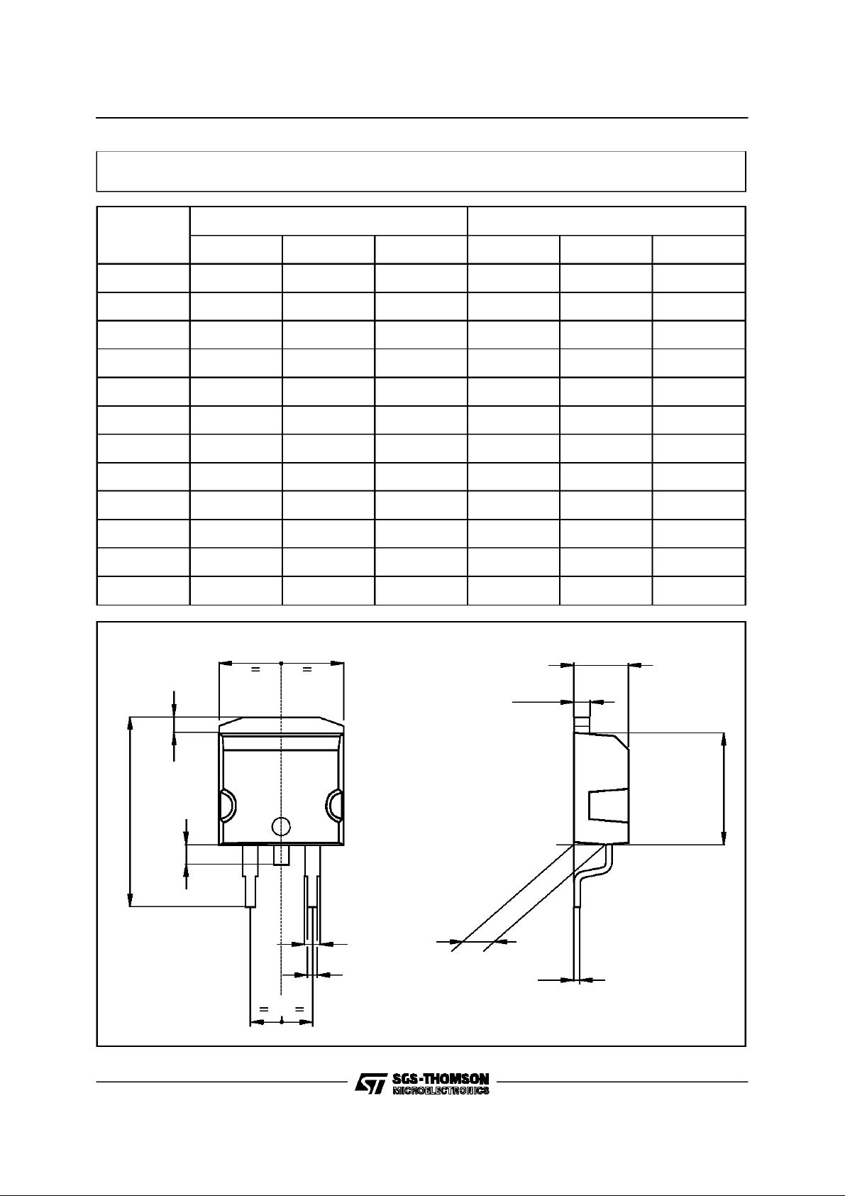
TO-263 (D2PAK) MECHANICAL DATA
STB19NB20
DIM.
MIN. TYP. MAX. MIN. TYP. MAX.
A 4.3 4.6 0.169 0.181
A1 2.49 2.69 0.098 0.106
B 0.7 0.93 0.027 0.036
B2 1.25 1.4 0.049 0.055
C 0.45 0.6 0.017 0.023
C2 1.21 1.36 0.047 0.053
D 8.95 9.35 0.352 0.368
E 10 10.28 0.393 0.404
G 4.88 5.28 0.192 0.208
L 15 15.85 0.590 0.624
L2 1.27 1.4 0.050 0.055
L3 1.4 1.75 0.055 0.068
mm inch
E
A
C2
L2
D
L
L3
B2
B
A1
C
G
P011P6/C
5/6
Page 6

STB19NB20
Informationfurnished is believedto be accurate and reliable. However, SGS-THOMSON Microelectronicsassumes no responsabilityfor the
consequencesof use of such information nor for any infringementof patents or other rights of third partieswhich may results fromits use. No
license is granted by implication or otherwise under anypatentor patentrights of SGS-THOMSONMicroelectronics. Specificationsmentioned
in this publication are subject to change without notice. This publicationsupersedesand replaces all informationpreviously supplied.
SGS-THOMSON Microelectronicsproducts arenotauthorizedfor useascriticalcomponentsinlifesupportdevicesorsystemswithoutexpress
written approvalof SGS-THOMSONMicroelectonics.
1997 SGS-THOMSONMicroelectronics -Printed in Italy- All Rights Reserved
Australia- Brazil - Canada- China- France- Germany- Hong Kong - Italy - Japan- Korea -Malaysia - Malta - Morocco - The Netherlands -
Singapore - Spain- Sweden - Switzerland- Taiwan - Thailand - UnitedKingdom- U.S.A
SGS-THOMSON MicroelectronicsGROUP OF COMPANIES
...
6/6
 Loading...