

Page 1
STB16NS25
N-CHANNEL 250V - 0.23Ω -16AD2PAK
MESH OVERLAY™ MOSFET
TYPE V
DSS
R
DS(on)
I
D
STB16NS25 250 V < 0.28 Ω 16 A
■ TYPICAL R
■ EXTREMELY HIGHdv/dt CAPABILITY
■ 100% AVALANCHE TESTED
(on) = 0.23 Ω
DS
DESCRIPTION
Using the latest high voltage MESH OVERLAY™
process, STMicroelectronics has designed an a dvanced family of power MOSFETs with outstanding
performance. The new patented STrip layout co upled with t he C ompany’s proprietary edge te rmin ation structure, makes it s uitable in coverters for
lighting applications.
APPLICATIONS
■ HIGH CURRENT, HIGH SPEED SWITCHING
■ SWITH MODE POWER SUPPLIES (SMPS)
■ DC-DC CONVERTERS FOR TELECOM,
INDUSTRIAL, AND LIGHTING EQUIPMENT
3
1
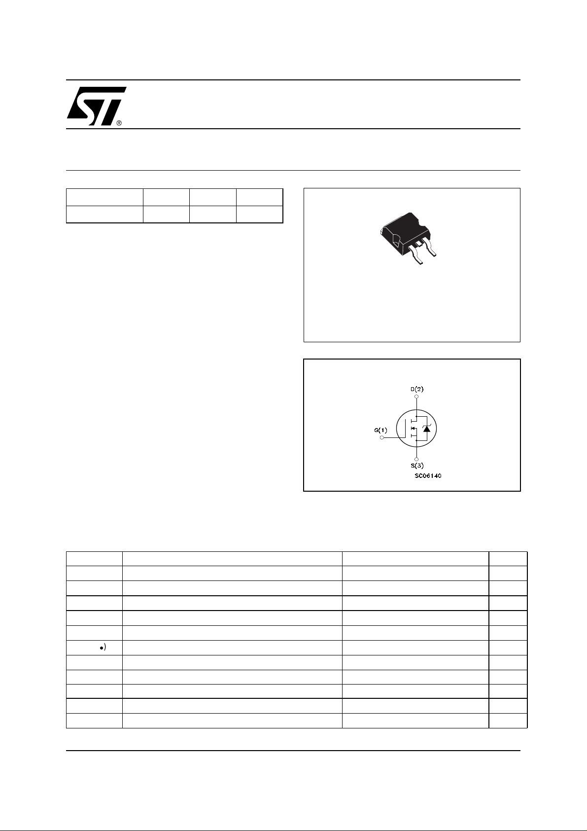
D2PAK
INTERNAL SCHEMATIC DIAGRAM
ABSOLUTE MAXIMUM RATINGS
Symbol Parameter Value Unit
V
DS
V
DGR
V
GS
I
D
I
D
IDM()
P
TOT
dv/dt (1) Peak Diode Recovery voltage slope 5 V/ns
T
stg
T
j
(•)Pulse width limited by safe operating area
Drain-source Voltage (VGS=0)
Drain-gate Voltage (RGS=20kΩ)
250 V
250 V
Gate- source Voltage ± 20 V
Drain Current (continuos) at TC= 25°C
Drain Current (continuos) at TC= 100°C
16 A
11 A
Drain Current (pulsed) 64 A
Total Dissipation at TC= 25°C
140 W
Derating Factor 1 W/°C
Storage Temperature –65 to 175 °C
Max. Operating Junction Temperature 175 °C
(1) ISD≤ 16A, di/dt≤300 A/µs, VDD≤ V
(BR)DSS
,Tj≤T
jMAX
1/9February 2003
Page 2
STB16NS25
THERMAL DATA
Rthj-case Thermal Resistance Junction-case Max 0.9 °C/W
Rthj-amb Thermal Resistance Junction-ambient Max 62.5 °C/W
T
l
AVALANCHE CHARACTERISTICS
Symbol Parameter Max Value Unit
I
AR
E
AS
ELECTRICAL CHARACTERISTICS (TCASE = 25 °C UNLESS OTHERWISE SPECIFIED)
OFF
Symbol Parameter Test Conditions Min. Typ. Max. Unit
V
(BR)DSS
I
DSS
I
GSS
Maximum Lead Temperature For Soldering Purpose 300 °C
Avalanche Current, Repetitive or Not-Repetitive
(pulse width limited by T
max)
j
Single Pulse Avalanche Energy
(starting T
Drain-source
= 25 °C, ID=IAR,VDD=28V)
j
ID= 250 µA, VGS= 0 250 V
16 A
200 mJ
Breakdown Voltage
= Max Rating
Zero Gate Voltage
Drain Current (V
GS
Gate-body Leakage
Current (V
DS
=0)
=0)
V
DS
= Max Rating, TC= 125 °C
V
DS
V
= ± 20 V ±100 nA
GS
1µA
50 µA
ON (1)
Symbol Parameter Test Conditions Min. Typ. Max. Unit
V
GS(th)
R
DS(on)
Gate Threshold Voltage
Static Drain-source On
V
DS=VGS,ID
VGS=10V,ID=8A
= 250µA
234V
0.23 0.28 Ω
Resistance
DYNAMIC
Symbol Parameter Test Conditions Min. Typ. Max. Unit
(1) Forward Transconductance VDS>I
g
fs
C
iss
C
oss
C
rss
Input Capacitance
Output Capacitance 190 pF
Reverse Transfer
Capacitance
D(on)xRDS(on)max,
ID=8A
V
=25V,f=1MHz,VGS=0
DS
14 15 S
1270 pF
75 pF
2/9
Page 3
STB16NS25
ELECTRICAL CHARACTERISTICS (CONTINUED)
SWITCHING ON
Symbol Parameter Test Conditions Min. Typ. Max. Unit
V
t
d(on)
Q
Q
Q
t
r
g
gs
gd
Turn-on Delay Time
Rise Time 25 ns
Total Gate Charge
Gate-Source Charge 8 nC
Gate-Drain Charge 22 nC
SWITCHING OFF
Symbol Parameter Test Conditions Min. Typ. Max. Unit
t
d(off)
t
t
r(Voff)
t
t
f
f
c
Turn-off- Delay Time
Fall Time
Off-voltage Rise Time
Fall Time
Cross-over Time
SOURCE DRAIN DIODE
Symbol Parameter Test Conditions Min. Typ. Max. Unit
I
SD
I
SDM
V
SD
t
rr
Q
rr
I
RRM
Note: 1. Pulsed: Pulse duration = 300 µs, duty cycle 1.5 %.
2. Pulse width limited by s afe operating area.
Source-drain Current 16 A
(2)
Source-drain Current (pulsed) 64 A
(1)
Forward On Voltage
Reverse Recovery Time
Reverse Recovery Charge 1.5 µC
Reverse Recovery Current 11.5 A
=125V,ID=8A
DD
R
= 4.7Ω VGS=10V
G
(see test circuit, Figure 3)
V
=200V,ID=16A,
DD
=10V
V
GS
VDD= 125V, ID=8A,
RG=4.7Ω, VGS= 10V
(see test circuit, Figure 3)
= 200V, ID=16A,
V
clamp
RG=4.7Ω, VGS= 10V
(see test circuit, Figure 5)
ISD=16A,VGS=0
I
= 16 A, di/dt = 100A/µs
SD
V
=33V,Tj= 150°C
DD
(see test circuit, Figure 5)
15 ns
60 80 nC
75
35
25
30
55
1.5 V
270 ns
ns
ns
ns
ns
ns
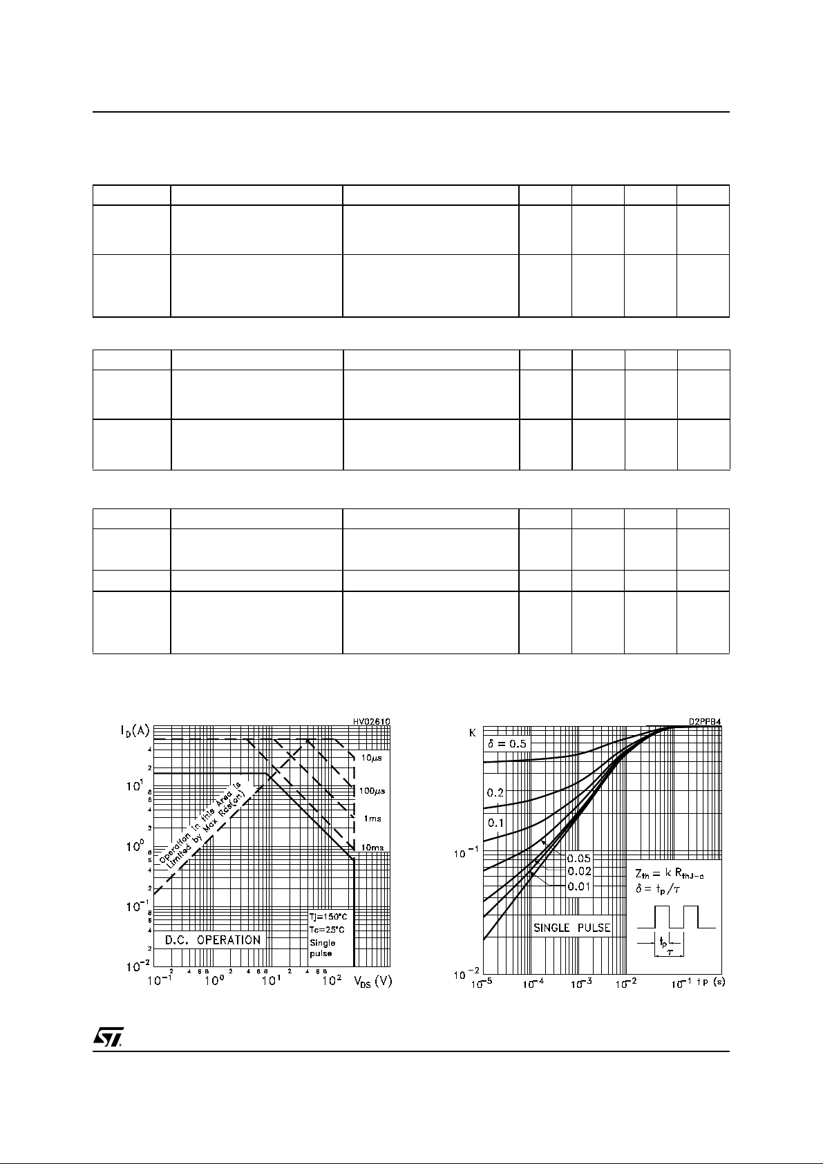
Thermal ImpedanceSafe Operati ng Area
3/9
Page 4
STB16NS25
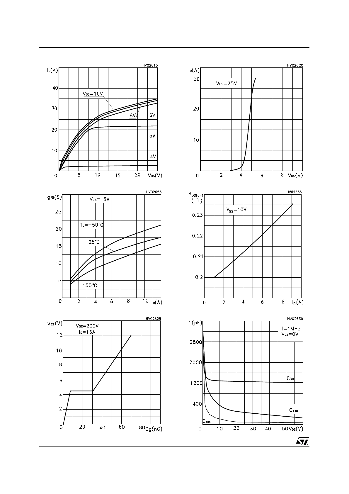
Transfer CharacteristicsOutput Characteristics
Transconductance
Gate Charge vs Gate-so urce Voltage
Static Drain-source On Resistance
Capacitance Variations
4/9
Page 5
STB16NS25
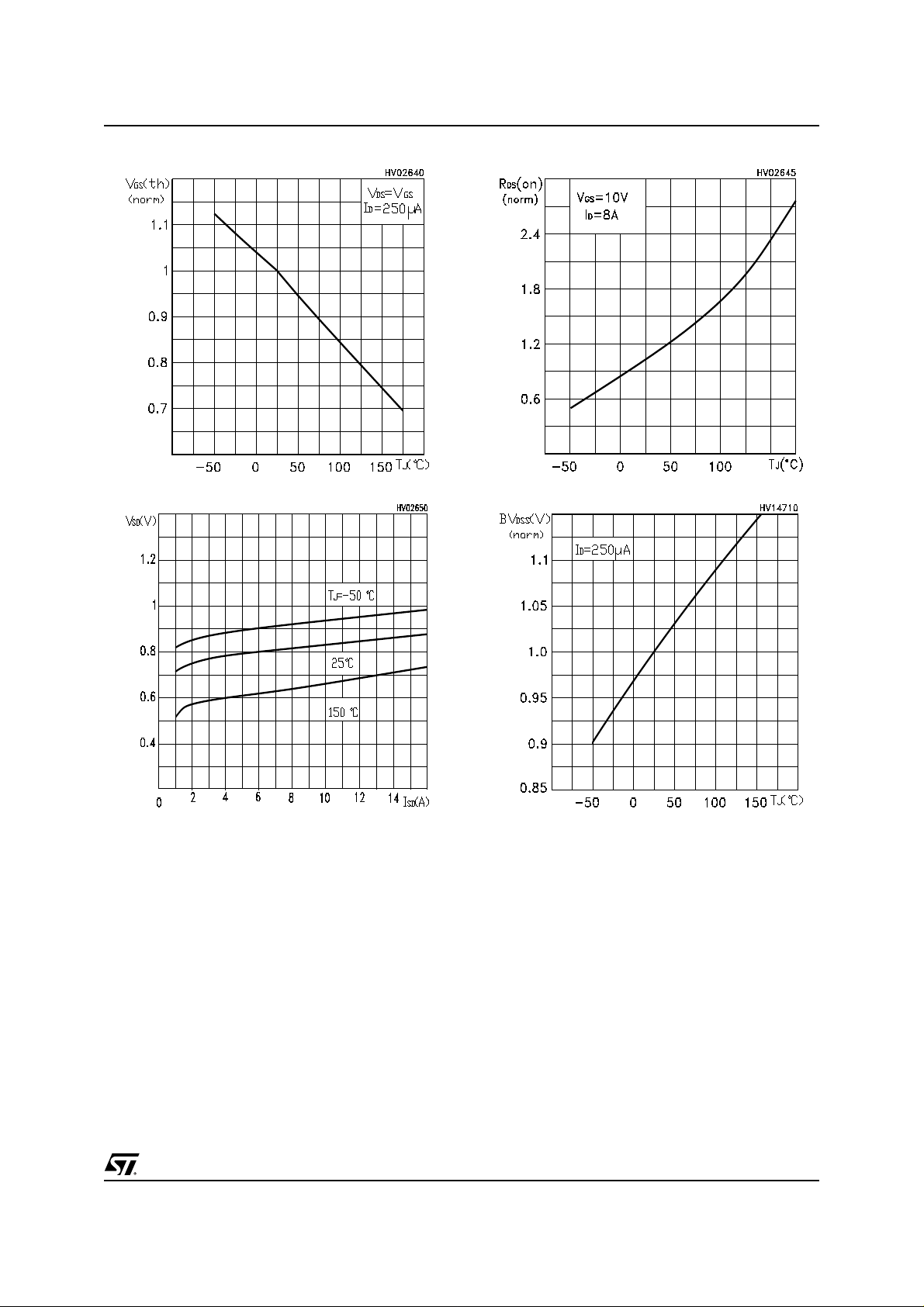
Normalized On Resistance vs Tem peratureNormalized Gate Theresho ld Voltage vs Temp.
Source-drain Diode Forward Characteristics
Normalized BVDSS vs Temperature
5/9
Page 6

STB16NS25
Fig. 2: Unclamped Inductive WaveformFig. 1: Unclamped Inductive Load Test Circuit
Fig. 3: Switching Times Test Circuit For
Resistive Loa d
Fig. 5: Test Circuit For Inductive Load Switching
And Diode Recovery Times
Fig. 4: Gate Charge test Circuit
6/9
Page 7
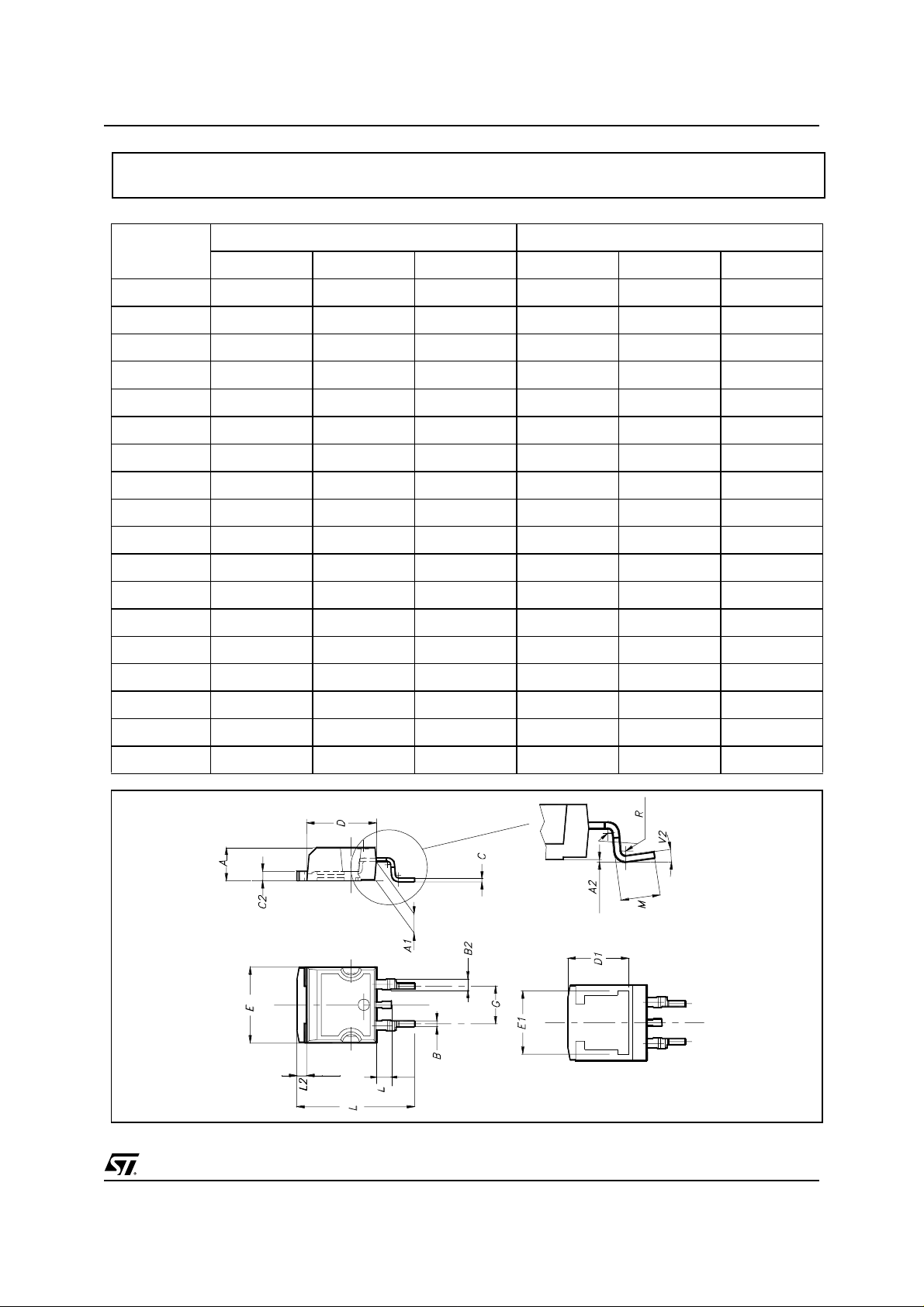
D2PAK MECHANICAL DATA
STB16NS25
DIM.
MIN. TYP MAX. MIN. TYP. MAX.
A 4.4 4.6 0.173 0.181
A1 2.49 2.69 0.098 0.106
A2 0.03 0.23 0.001 0.009
B 0.7 0.93 0.027 0.036
B2 1.14 1.7 0.044 0.067
C 0.45 0.6 0.017 0.023
C2 1.23 1.36 0.048 0.053
D 8.95 9.35 0.352 0.368
D1 8 0.315
E 10 10.4 0.393
E1 8.5 0.334
G 4.88 5.28 0.192 0.208
L 15 15.85 0.590 0.625
L2 1.27 1.4 0.050 0.055
L3 1.4 1.75 0.055 0.068
mm. inch
M 2.4 3.2 0.094 0.126
R 0.4 0.015
V2 0º 4º
3
7/9
1
Page 8
STB16NS25
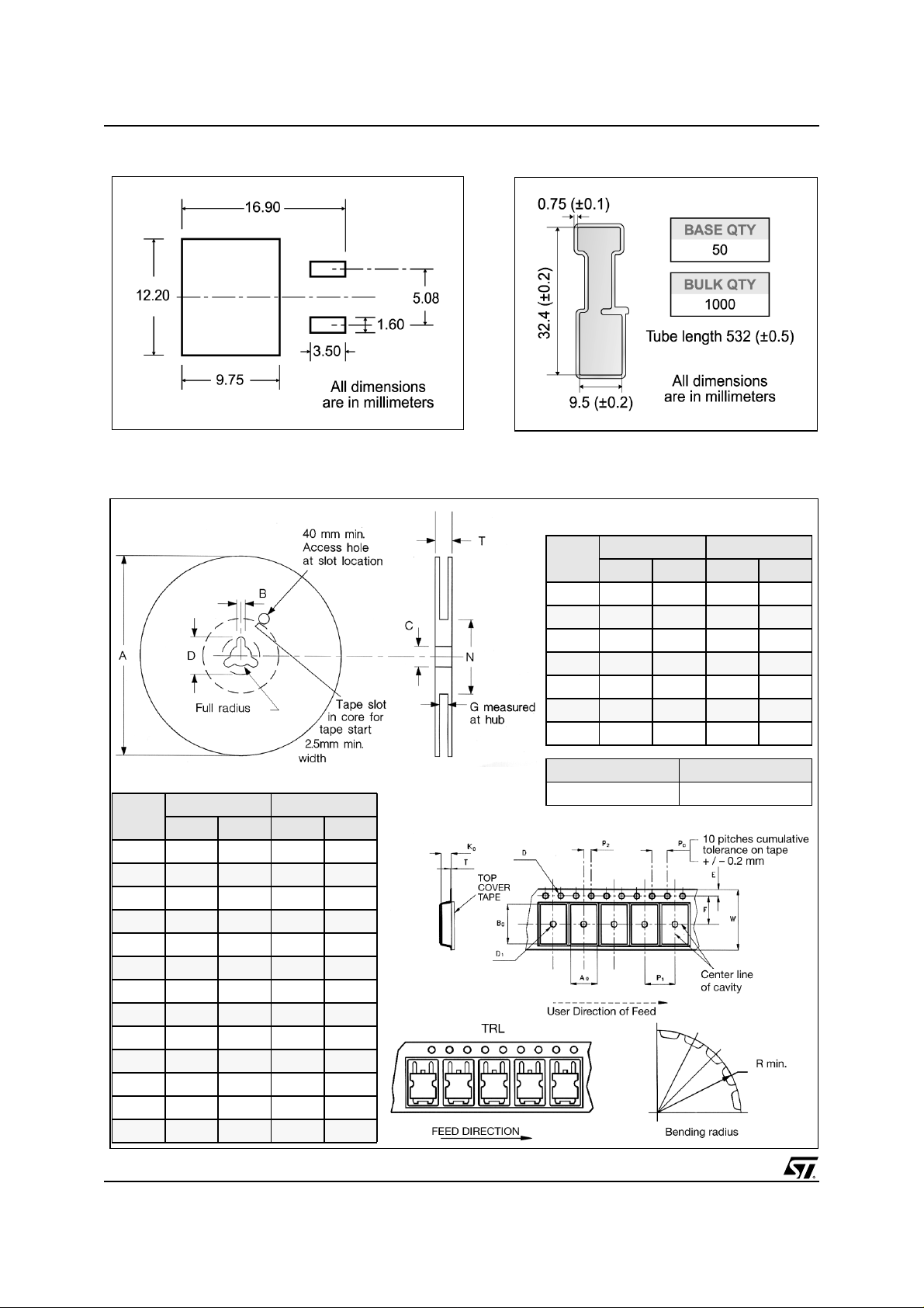
D2PAK FOOTPRINT
TAPE AND REEL SHIPMENT (suffix ”T4”)*
TUBE SHIPMENT (no suffix)*
REEL MECHANICAL DATA
DIM.
A 330 12.992
B 1.5 0.059
C 12.8 13.2 0.504 0.520
D 20.2 0795
G 24.4 26.4 0.960 1.039
N 100 3.937
T 30.4 1.197
mm inch
MIN. MAX. MIN. MAX.
TAPE MECHANICAL DATA
DIM.
A0 10.5 10.7 0.413 0.421
B0 15.7 15.9 0.618 0.626
D 1.5 1.6 0.059 0.063
D1 1.59 1.61 0.062 0.063
E 1.65 1. 85 0.065 0.073
F 11.4 11.6 0.449 0.456
K0 4.8 5.0 0.189 0.197
P0 3.9 4.1 0.153 0.161
P1 11.9 12.1 0.468 0.476
P2 1.9 2.1 0.075 0.082
R 50 1.574
T 0.25 0.35 0.0098 0.0137
W 23.7 24.3 0.933 0.956
* on sales ty pe
8/9
mm inch
MIN. MAX. MIN. MAX.
BASE QTY BULK QTY
1000 1000
Page 9

STB16NS25
Information furnished is believed to be accurate and reliable. However, STMicroelectronics assumes no responsibility for the
consequences of u se of such inf ormat ion nor for any in fring ement of p aten ts or othe r ri ghts of th ird p arties whic h may resul t f rom
its use. No license is granted by implication or otherwise under any patent or patent rights of STMicroelectronics. Specifications
mentioned in this publication are subject to change without notice. This publication supersedes and replaces all information
previously supplied. STMicroelectronics products are not authorized for use as critical components in life support devices or
systems without express written approval of STMicroelectronics.
Australia - Brazil - Canada - China - Finland - France - Germany - Hong Kong - India - Israel - Italy - Japan - Malaysia - Malta - Morocco
© The ST logo is a registered trademark of STMicroelectronics
© 2003 STMicroelectronics - Printed in Italy - All Rights Reserved
Singapore - Spain - Sweden - Switzerland - United Kingdom - United States.
STMicroelectronics GROUP OF COMPANIES
© http://www.st.com
9/9
 Loading...