

Page 1
STB16NF06L
N-CHANNEL 60V - 0.07 Ω - 16A D2PAK
STripFET™ POWER MOSFET
TYPE
V
DSS
STB16NF06L 60 V <0.09
■ TYPICAL R
■ EXCEPTIONA L dv/d t CAPABILITY
■ LOW GATE CHARGE AT 100
■ LOW THRESHOLD DRIVE
■ SURFACE-MOUNTING D
(on) = 0.07Ω
DS
R
DS(on)
Ω
o
C
2
PAK (TO-263)
I
D
16 A
POWER PACKAG E IN TU BE (NO SU FFIX) OR
IN TAPE & REEL (SUFFIX “T4”)
DESCRIPTION
This Power MOSFET is the latest development of
STMicroelectron is unique "Single Feature Size™" str ipbased process . The res ulting tran sistor sho ws extrem ely
high packing density for low on-resistance, rugged
avalanche characteristics and less critical alignment
steps therefore a remarkable manufacturing
reproducibility.
APPLICATIONS
■ MOTOR CONTROL, AUDIO AMPLIFIERS
■ HIGH CURRENT, HIGH SPEED SWITCHING
■ SOLENOID AND RELAY DRIVERS
■ DC-DC & DC-AC CONVERTERS
■ AUTOMOTIVE ENVIRONMENT
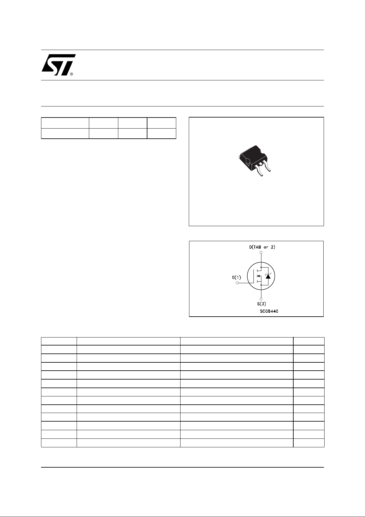
3
1
D2PAK
TO-263
(Suffix “T4”)
INTERNAL SCHEMATIC DIAGRAM
ABSOLUTE MAXIMUM RATINGS
Symbol Parameter Value Unit
V
DS
V
DGR
V
GS
I
D
I
D
(
I
DM
P
tot
dv/dt
E
AS
T
stg
T
j
(
Pulse width l i mited by safe operating area. (1) ISD ≤ 16A, di/dt ≤ 210A/µs , VDD ≤ V
•)
.
Drain-source Voltage (VGS = 0)
Drain-gate Voltage (RGS = 20 kΩ)
60 V
60 V
Gate- source Voltage ± 16 V
Drain Current (continuos) at TC = 25°C
Drain Current (continuos) at TC = 100°C
•)
Drain Current (pulsed) 64 A
Total Dissipation at TC = 25°C
16 A
11 A
45 W
Derating Factor 0.3 W/°C
(1)
Peak Diode Recovery voltage slope 23 V/ns
(2)
Single Pulse Avalanche Energy 127 mJ
Storage Temperature -65 to 175 °C
Max. Operating Junction Temperature -55 to 175 °C
(2) Starting Tj = 25 oC, ID = 8A, VDD = 30V
(BR)DSS
, Tj ≤ T
JMAX.
1/9February 2002
Page 2
STB16NF06L
THERMA L D ATA
Rthj-case
Rthj-amb
T
Thermal Resistance Junction-case
Thermal Resistance Junction-ambient
Maximum Lead Temperature For Soldering Purpose
j
Max
Max
Typ
3.33
62.5
300
°C/W
°C/W
°C
ELECTRICAL CHARACTERISTICS (T
= 25 °C unless otherwise specified)
case
OFF
Symbol Parameter Test Conditions Min. Typ. Max. Unit
I
V
(BR)DSS
Drain-source
= 250 µA, VGS = 0
D
60 V
Breakdown Voltage
V
= Max Rating
DS
V
= Max Rating TC = 125°C
DS
V
= ± 16V
GS
1
10
±100 nA
ON
(1)
I
DSS
I
GSS
Zero Gate Voltage
Drain Current (V
GS
Gate-body Leakage
Current (V
DS
= 0)
= 0)
Symbol Parameter Test Conditions Min. Typ. Max. Unit
V
V
GS(th)
R
DS(on)
Gate Threshold Voltage
Static Drain-source On
Resistance
= VGS I
DS
= 5 V ID = 8 A
V
GS
V
= 10 V ID = 8 A
GS
= 250 µA
D
1V
0.08
0.07
0.10
0.09
DYNAMIC
Symbol Parameter Test Conditions Min. Typ. Max. Unit
(*)
g
fs
C
iss
C
oss
C
rss
Forward Transconductance
Input Capacitance
Output Capacitance
Reverse Transfer
Capacitance
> I
V
I
D
V
DS
=8 A
DS
x R
D(on)
DS(on)max,
= 25V, f = 1 MHz, VGS = 0
17 S
345
72
29
µA
µA
Ω
Ω
pF
pF
pF
2/9
Page 3
STB16NF06L
ELECTRICAL CHARACTERISTICS (continued)
SWITCHING ON
Symbol Parameter Test Conditions Min. Typ. Max. Unit
= 30 V ID = 8 A
t
d(on)
Turn-on Delay Time
t
r
Rise Time
V
DD
R
= 4.7 Ω VGS = 4.5 V
G
(Resistive Load, Figure 3)
Q
g
Q
gs
Q
gd
Total Gate Charge
Gate-Source Charge
Gate-Drain Charge
= 48 V ID = 16 A VGS= 5V
V
DD
SWITCHING OFF
Symbol Parameter Test Conditions Min. Typ. Max. Unit
= 30 V ID = 8 A
t
d(off)
Turn-off Delay Time
t
f
Fall Time
V
DD
R
= 4.7Ω, V
G
GS
= 4.5 V
(Resistive Load, Figure 3)
SOURCE DRAIN DIODE
Symbol Parameter Test Conditions Min. Typ. Max. Unit
I
SD
I
SDM
V
SD
t
rr
Q
rr
I
RRM
(*)
Pulsed: P ul se duration = 300 µs, duty cycle 1.5 %.
(
•)Pulse width limited by safe operating area.
Source-drain Current
(•)
Source-drain Current (pulsed)
(*)
Forward On Voltage
Reverse Recovery Time
Reverse Recovery Charge
Reverse Recovery Current
I
= 16 A VGS = 0
SD
= 16 A di/dt = 100A/µs
I
SD
V
= 16 V Tj = 150°C
DD
(see test circuit, Figure 5)
10
37
7.3
2.1
3.1
20
12.5
50
67.5
2.7
10 nC
16
64
1.3 V
ns
ns
nC
nC
ns
ns
A
A
ns
nC
A
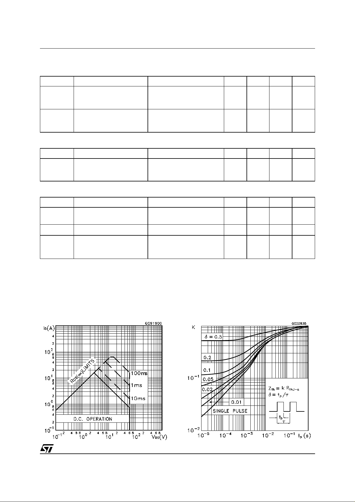
Safe Operating Area Thermal Impedance
3/9
Page 4

STB16NF06L
Output Characteristics Transfer Characteristics
Transconductance Static Drain-source On Resistance
Gate Charge vs Gate-source Voltage Capacitance Variations
4/9
Page 5

STB16NF06L
Normalized Gate Threshold Voltage vs Temperature Normalized on Resistance vs Temperature
Source-drain Diode Forward Characteristics
. .
.
5/9
Page 6

STB16NF06L
Fig. 1: Unclamped Inductive Load Test CircuitFig. 1: Unclamped Inductive Load Test Circuit Fig. 2: Unclamped Inductive Waveform
Fig. 3: Switching Times Test Circuits For Resistive
Load
Fig. 5: Test Circuit For Inductive Load Switching
And Diode Recovery Times
Fig. 4: Gate Charge test Circuit
6/9
Page 7

D2PAK MECHANICAL DA TA
STB16NF06L
DIM.
A 4.4 4.6 0.173 0.181
A1 2.49 2.69 0.098
A2 0.03 0.23 0.001 0.009
B 0.7 0.93 0.028 0.037
B2 1.14 1.7 0.045 0.067
C 0.45 0.6 0.018 0.024
C2 1.21 1.36 0.048 0.054
D 8.95 9.35 0.352 0.368
D1 8 0.315
E 10 10.4 0.394 0.409
E1 8.5 0.334
G 4.88 5.28 0.192 0.208
L 15 15.85 0.591 0.624
L2 1.27 1.4 0.050 0.055
L3 1.4 1.75 0.055 0.069
M 2.4 3.2 0.094 0.126
R 0.4 0.016
V2 0° 8° 0° 8°
MIN. TYP. MAX. MIN. TYP. TYP.
mm. inch.
0.106
7/9
Page 8

STB16NF06L
D2PAK FOOTPRINT
TAPE AND REEL SHIPMENT (suffix ”T4”)*
TUBE SHIPMENT (no suffix)*
REEL MECHANICAL DATA
DIM.
A 330 12.992
B 1.5 0.059
C 12.8 13.2 0.504 0.520
D 20.2 0.795
G 24.4 26.4 0.960 1.039
N 100 3.937
T 30.4 1.197
mm inch
MIN. MAX. MIN. MAX.
TAPE MECHANICAL DATA
DIM.
A0 10.5 10.7 0.413 0.421
B0 15.7 15.9 0.618 0.626
D 1.5 1.6 0.059 0.063
D1 1.59 1.61 0.062 0.063
E 1.65 1.85 0.065 0.073
F 11.4 11.6 0.449 0.456
K0 4.8 5.0 0.189 0.197
P0 3.9 4.1 0.153 0.161
P1 11.9 12.1 0.468 0.476
P2 1.9 2.1 0075 0.082
R50 1.574
T0.25 0.35 .0.0098 0.0137
W 23.7 24.3 0.933 0.956
mm inch
MIN. MAX. MIN. MAX.
* on sales type
8/9
BASE QTY BULK QTY
1000 1000
Page 9

STB16NF06L
Information furnished is believed to be ac curate and reliable. Howev er, STMicroelec tronics assumes no responsibility for t he consequ ences
of use of such information nor for any infringement of patents or other rights of third parties which may result from its use. No license is granted
by implic ation or oth erwise under any patent or patent rights of STMicroelectron i cs . Specificat i ons mentioned in thi s publication are subject
to change without notice. This publication supersedes and replaces all information previously supplied. STMicroelectronics products are not
authorized for use as critical comp onents in life support devices or systems wi thout express written approval of STM i croelect ronics.
The ST log o i s registered trademark of STM icroelec tronics
2002 STMi croelectr oni cs - All Righ t s Reserved
All other names are the property of their respective owner s.
Australi a - Brazil - Canada - China - F i nl and - France - Germany - Hong Kong - India - Israel - Italy - Japan - Mal aysia - Malta - Morocco -
Singapor e - S pai n - Sweden - Swi t zerland - Uni t ed Kingdom - U ni t ed States.
STMicroelect ro n ics GRO UP OF COMPANI ES
http://www.st.com
9/9
 Loading...