

Page 1
ST13005
HIGH VOLTAGE FAST-SWITCHING
■ MEDIUMVOLTAGECAPABILITY
■ NPNTRANSISTORS
■ LOW SPREADOF DYNAMICPARAMETERS
■ MINIMUMLOT-TO-LOT SPREAD FOR
RELIABLEOPERATION
■ VERYHIGH SWITCHING SPEED
■ THROUGH-HOLE I2PAK (TO-262)POWER
PACKAGEIN TUBE(SUFFIX ”-1”)
APPLICATIONS:
■ ELECTRONICBALLASTSFOR
FLUORESCENT LIGHTING
■ SWITCHMODEPOWER SUPPLIES
DESCRIPTION
The devices are is manufactured using high
voltage Multi Epitaxial Planar technology for high
switchingspeeds and medium voltage capability.
They use a Cellular Emitter structure with planar
edge termination to enhance switching speeds
while maintainingthe wide RBSOA.
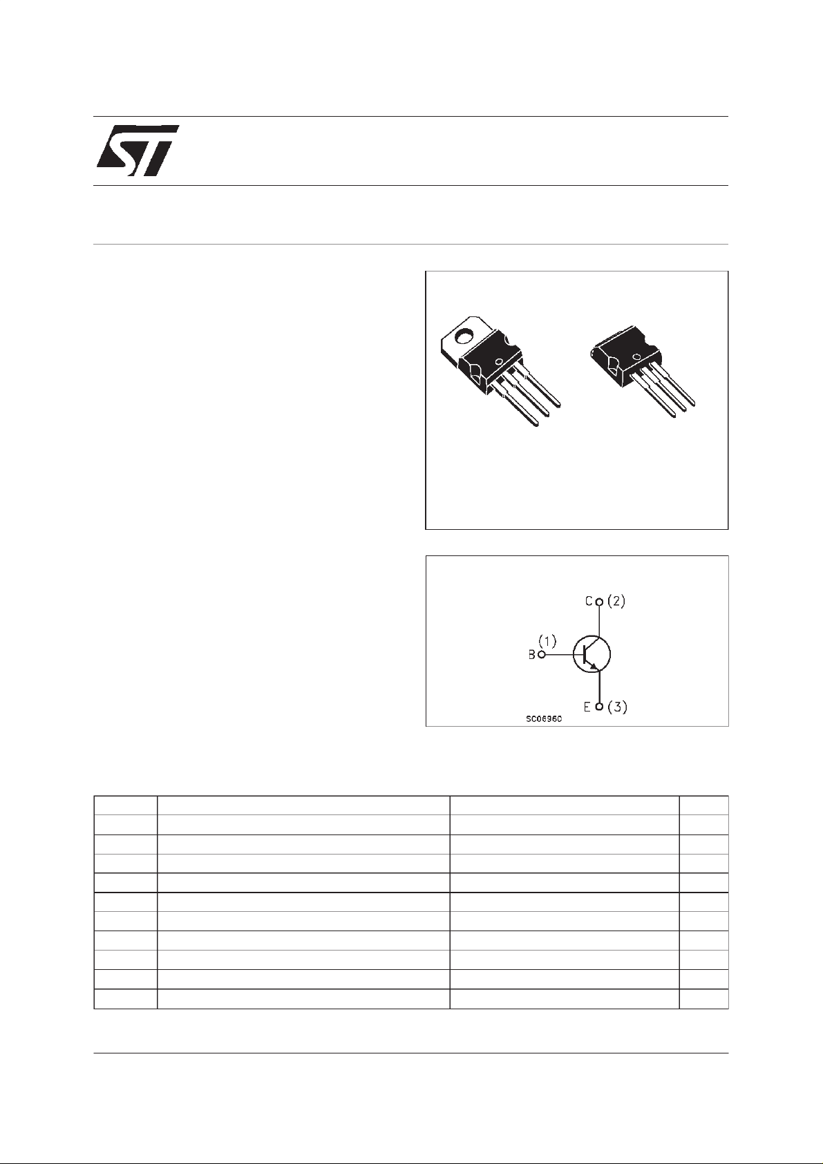
STB13005-1
NPN POWER TRANSISTORS
3
2
1
TO-220 I2PAK
TO-262
(Suffix ”-1”)
INTERNAL SCHEMATIC DIAGRAM
3
2
1
ABSOLUTE MAXIMUM RATINGS
Symbol Parameter Value Unit
V
V
V
I
I
P
T
January 1999
Collect or-Emit t e r V oltage (VBE= 0 ) 700 V
CES
Collect or-Emit t e r V oltage (IB= 0 ) 400 V
CEO
Emitter-Base Volt age (IC=0) 9 V
EBO
Collect or Current 4 A
I
C
Collect or Peak Cur rent (tp<5ms) 8 A
CM
I
Base Current 2 A
B
Base P eak Current (tp<5ms) 4 A
BM
Tot al Dissipa t io n at Tc=25oC75W
tot
Storage Temperature -65 to 150
stg
Max. Ope rating Junct ion Temperature 150
T
j
o
C
o
C
1/8
Page 2
ST13005 / STB13005-1
THERMAL DATA
R
thj-case
Ther mal Resis t an c e Junc t ion-case M ax 1.67
o
C/W
ELECTRICAL CHARACTERISTICS (T
=25oC unlessotherwise specified)
case
Symbol Parameter Test Cond itions Min. Typ. Max. Un it
I
CEV
I
EBO
V
CEO(sus)
Collec t or Cut -off
Current (V
=-1.5V)
BE
Emitter Cut-off
Current (I
C
=0)
∗ Collec t or-Emit t er
V
= 700V
CE
= 700V T
V
CE
V
=9V 1 mA
EB
I
= 10 mA 400 V
C
case
= 100oC
1
5
mA
mA
Sust aining Voltage
=0)
(I
B
∗ Collec t or -Emitt er
V
CE(sat)
Saturation Voltage
V
∗ Base-Emi tter
BE(sat)
Saturation Voltage
h
DC Current Ga in IC=1A VCE=5V
FE
IC=1A IB=0.2A
=2A IB=0.5A
I
C
I
=4A IB=1A
C
IC=1A IB=0.2A
=2A IB=0.5A
I
C
Gr oup A
Gr oup B
=2A VCE=5V
I
C
15
27
0.5
0.6
1
1.2
1.6
32
45
8
40
V
V
V
V
RESI STIVE LOAD
t
∗
Pulsed: Pulse duration = 300µs, duty cycle = 1.5 %
Note : Product is pre-selected in DC current gain (GROUP A and GROUP B).STMicroelectronics reserves the right to ship either groups
according to production availability. Please contact your nearest STMicroelectronics sales office for delivery details.
s
t
f
Storage Time
Fall Time
=2A
I
C
=-IB2=0.4A
I
B1
=125V Tp=30µs
V
CC
1.5
0.2
3.0 µs
µs
2/8
Page 3
ST13005 / STB13005-1
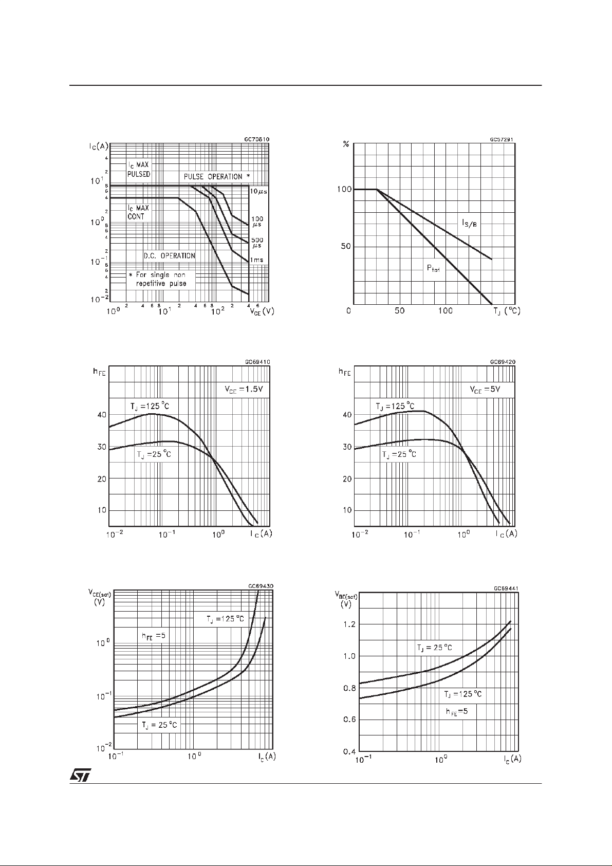
Safe Operating Areas
DCCurrent Gain
DeratingCurve
DC Current Gain
CollectorEmitterSaturationVoltage
BaseEmitter Saturation Voltage
3/8
Page 4

ST13005 / STB13005-1
InductiveFall Time InductiveStorage Time
ResistiveFall Time Resistive Load Storage Time
ReverseBiased SOA
4/8
Page 5

Figure1: Inductive Load Switching TestCircuit.
1) Fas t elect ronic swit ch
2) Non-inductive Resistor
3) Fast recovery rectifier
Figure2: Resistive Load Switching Test Circuit.
ST13005 / STB13005-1
1) Fas t elect ronic swit ch
2) Non-inductive Resistor
5/8
Page 6

ST13005 / STB13005-1
TO-220 MECHANICAL DATA
DIM.
MIN. TYP. MAX. MIN. TYP. MAX.
A 4.40 4.60 0.173 0.181
C 1.23 1.32 0.048 0.051
D 2.40 2.72 0.094 0.107
D1 1.27 0.050
E 0.49 0.70 0.019 0.027
F 0.61 0.88 0.024 0.034
F1 1.14 1.70 0.044 0.067
F2 1.14 1.70 0.044 0.067
G 4.95 5.15 0.194 0.203
G1 2.4 2.7 0.094 0.106
H2 10.0 10.40 0.393 0.409
L2 16.4 0.645
L4 13.0 14.0 0.511 0.551
L5 2.65 2.95 0.104 0.116
L6 15.25 15.75 0.600 0.620
L7 6.2 6.6 0.244 0.260
L9 3.5 3.93 0.137 0.154
DIA. 3.75 3.85 0.147 0.151
mm inch
6/8
P011C
Page 7

TO-262 (I2PAK) MECHANICAL DATA
ST13005 / STB13005-1
DIM.
MIN. TYP. MAX. MIN. TYP. MAX.
A 4.4 4.6 0.173 0.181
A1 2.49 2.69 0.098 0.106
B 0.7 0.93 0.027 0.036
B2 1.14 1.7 0.044 0.067
C 0.45 0.6 0.017 0.023
C2 1.23 1.36 0.048 0.053
D 8.95 9.35 0.352 0.368
e 2.4 2.7 0.094 0.106
E 10 10.4 0.393 0.409
L 13.1 13.6 0.515 0.531
L1 3.48 3.78 0.137 0.149
L2 1.27 1.4 0.050 0.055
mm inch
CA1
A
C2
B2
B
e
E
L1
L2
D
L
P011P5/E
7/8
Page 8

ST13005 / STB13005-1
Information furnished is believed tobe accurate and reliable. However, STMicroelectronics assumes no responsibility for the consequences
of use of such information nor for any infringement of patents or other rights of third parties which may result from its use. No license is
granted by implication or otherwise under any patent or patent rights of STMicroelectronics. Specification mentioned in this publication are
subject to change without notice. This publication supersedes and replaces all information previously supplied. STMicroelectronics products
are not authorized for use as critical components in life support devices or systems without express written approval of STMicroelectronics.
The ST logo is a registered trademark of STMicroelectronics
1998 STMicroelectronics – Printed in Italy – All Rights Reserved
STMicroelectronicsGROUP OF COMPANIES
Australia - Brazil -Canada - China -France - Germany - Italy - Japan - Korea - Malaysia - Malta - Mexico - Morocco - The Netherlands-
Singapore - Spain -Sweden - Switzerland - Taiwan - Thailand - UnitedKingdom - U.S.A.
http://www.st.com
.
8/8
 Loading...