

Datasheet STW14NM50FD, STP12NM50FDFP, STP12NM50FD, STB12NM50FD-1, STB12NM50FD Datasheet (SGS Thomson Microelectronics)
Page 1
STP12NM50FD-STP12NM50FDFP-STW14NM50FD
STB12NM50FD - STB12NM50FD-1
N-CHANNEL500V-0.32Ω-12ATO-220/FP/D2PAK/I2PAK/TO-247
FDmesh™ Power MOSFET (with FAST DIODE)
TYPE V
STP12NM50 FD
STP12NM50 FDFP
STB12NM50 FD
STB12NM50 FD-1
STW14NM50 FD
■ TYPICAL R
■ HIGH dv/dt AND AVALANCHE CAPABILITIES
■ 100% AVALANCHE TESTED
■ LOW INPUT CAPACITANCE AND GATE
500 V
500 V
500 V
500 V
500 V
(on) = 0.32 Ω
DS
DSS
R
DS(on)
< 0.4 Ω
< 0.4 Ω
< 0.4 Ω
< 0.4 Ω
< 0.4 Ω
I
D
12 A
12 A
12 A
12 A
14 A
Pw
160 W
35 W
160 W
160 W
175 W
CHARGE
■ LOW GATE INPUT RESIST ANC E
■ TIGHT PROCESS CONTROL AND HIGH
MANUFACTURING YIELDS
DESCRIPTION
The FDmesh™
associates all advantages of re-
duced on-resistance and fast swi tching with an intrinsic fast-recovery body diode. It is therefore
strongly recommended for bridge topologies, in particular ZVS phase-shift converters.
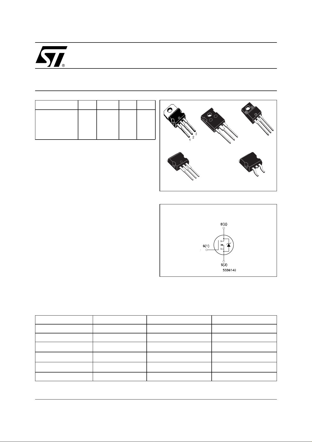
3
2
TO-220 TO-220FP
1
TO-247
3
I2PAK
3
2
1
D
2
PAK
1
INTERNAL SCHEMATIC DIAGRAM
3
2
1
APPLICATIONS
■ ZVS PHASE-SHIFT FULL BRIDGE
CONVERTERS FOR SMPS AND WELDING
EQUIPMENT
ORDERING INFORMATION
SALES TYPE MARKING PACKAGE PACKAGING
STP12NM50FD P12NM50FD TO-220 TUBE
STP12NM50FDFP P12NM50FDFP TO-220FP TUBE
STB12NM50FD B12NM50FD
STB12NM50FDT4 B12NM50FD
STB12NM50FD-1 B12NM50FD
STW14NM50FD W14NM50FD TO-247 TUBE
2
PAK
D
2
D
PAK
2
I
PAK
TUBE
TAPE & REEL
TUBE
1/14June 2002
Page 2
STP12NM50FD / STP12NM50FDFP / STB12NM50FD / STB12NM50FD-1 / STW14NM50FD
ABSOLUTE MAXIMUM RATINGS
Symbol Parameter Value Unit
TO-220 /
2
PAK / I2PAK
D
V
I
DM
P
V
V
DS
DGR
GS
I
D
I
D
TOT
Drain-source Voltage (VGS = 0)
Drain-gate Voltage (RGS = 20 kΩ)
Gate- source Voltage ± 30 V
Drain Current (continuous) at TC = 25°C
Drain Current (continuous) at TC = 100°C
(l)
Drain Current (pulsed) 48 48 (*) 56 A
Total Dissipation at TC = 25°C
12 12 (*) 14 A
7.5 7.5 (*) 8.8 A
160 35 175 W
Derating Factor 1.28 0.28 1.4 W/°C
dv/dt (1) Peak Diode Recovery voltage slope 20 V/ns
V
ISO
T
j
T
stg
(l) Pulse wi dth limited by saf e operating area
(1) I
≤12A, di/dt ≤ 400 µA, VDD ≤ V
SD
(*) Limited only by maximum temperature allowed
Insulation Withstand Voltage (DC) - 2500 V
Operating Junction Temperature
Storage Temperature
, Tj ≤ T
(BR)DSS
JMAX.
TO-220FP TO-247
500 V
500 V
- 65 to 150
- 65 to 150
°C
°C
THERMA L D ATA
TO-220
2
PAK
I
Rthj-case Thermal Resistance Junction-case Max 0.78 3.57 0.715 °C/W
Rthj-pcb Thermal Resistance Junction-pcb Max
(When mounted on minimum Footprint)
Rthj-amb Thermal Resistance Junction-ambient Max 62.5 30 °C/W
T
l
Maximum Lead Temperature For Soldering Purpose
2
D
TO-220FP TO-247
PAK
30 °C/W
300 °C
AVALANCHE CHARACTERISTICS
Symbol Parameter Max Value Unit
I
AR
Avalanche Current, Repetitive or Not-Repetitive
(pulse width limited by T
E
AS
Single Pulse Avalanche Energy
(starting T
max)
j
= 25 °C, ID = IAR, VDD = 50 V)
j
6A
400 mJ
2/14
Page 3

STP12NM50FD / STP12NM50FDFP / STB12NM50FD / STB12NM50FD-1 / STW14NM50FD
ELECTRICAL CHARACTERISTICS (TCASE =25°C UNLESS OTHERWISE SPECIFIED)
ON/OFF
Symbol Parameter Test Conditions Min. Typ. Max. Unit
V
(BR)DSS
Drain-source
Breakdown Voltage
I
DSS
I
GSS
V
GS(th)
R
DS(on)
Zero Gate Voltage
Drain Current (V
GS
= 0)
Gate-body Leakage
Current (V
DS
= 0)
Gate Threshold Voltage
Static Drain-source On
Resistance
DYNAMIC
Symbol Parameter Test Conditions Min. Typ. Max. Unit
g
(1) Forward Transconductance VDS = 15 V, ID= 6 A 9.8 S
fs
C
iss
C
oss
C
rss
R
G
Input Capacitance
Output Capacitance
Reverse Transfer
Capacitance
Gate Input Resistance f=1 MHz Gate DC Bias = 0
SWITCHING ON
Symbol Parameter Test Conditions Min. Typ. Max. Unit
t
d(on)
Q
Q
Q
t
r
g
gs
gd
Turn-on Delay Time
Rise Time
Total Gate Charge
Gate-Source Charge
Gate-Drain Charge
ID = 1 mA, VGS = 0 500 V
V
= Max Rating
DS
VDS = Max Rating, TC = 125 °C
V
= ± 30V ±100 nA
GS
V
= VGS, ID = 250µA
DS
345V
10
1
µA
µA
VGS = 10V, ID = 6A 0.32 0.4 Ω
= 25V, f = 1 MHz, VGS = 0 1027
V
DS
205
24
pF
pF
pF
3.7 Ω
Test Signal Level = 20mV
Open Drain
VDD = 250 V, ID = 6 A
R
= 4.7Ω VGS = 10 V
G
19
10
(Resistive Load see, Figure 3)
= 400V, ID = 12 A,
V
DD
VGS = 10V
27.5
8
12
38.5
nC
nC
nC
ns
ns
SWITCHING OFF
Symbol Parameter Test Conditions Min. Typ. Max. Unit
= 400 V, ID = 12 A,
t
r(Voff)
t
t
Off-voltage Rise Time
f
c
Fall Time
Cross-over Time
V
DD
R
=4.7Ω, V
G
GS
= 10V
(Inductive Load see, Figure 5)
39
18
29
SOURCE DRAIN DIODE
Symbol Parameter Test Conditions Min. Typ. Max. Unit
I
SD
I
SDM
VSD (1)
t
rr
Q
rr
I
RRM
Note: 1. Pulsed: Pu l se duration = 300 µs, duty c yc l e 1.5 %.
2. Pulse width li mited by safe operating area.
Source-drain Current
(2)
Source-drain Current (pulsed)
Forward On Voltage
Reverse Recovery Time
Reverse Recovery Charge
Reverse Recovery Current
ISD = 12 A, VGS = 0
I
SD
VDD = 30V, Tj = 150°C
(see test circuit, Figure 5)
= 12 A, di/dt = 100A/µs
224
1.3
12
12
48
1.5 V
ns
ns
ns
A
A
ns
µC
A
3/14
Page 4

STP12NM50FD / STP12NM50FDFP / STB12NM50FD / STB12NM50FD-1 / STW14NM50FD
Safe Operating Area For TO-220/D2PAK/I2PAK
Safe Operating Area For TO-220FP
Thermal Impedance For TO-220/D2PAK/I2PAK
Thermal Impedance For TO-220FP
Safe Operating Area For TO-247
4/14
Thermal Impedance For TO-247
Page 5

STP12NM50FD / STP12NM50FDFP / STB12NM50FD / STB12NM50FD-1 / STW14NM50FD
Output Characteristics
Transconductance Static Drain-source On Resistance
Transfer Characteristics
Gate Charge vs Gate-source Voltage Capacitance Var iations
5/14
Page 6

STP12NM50FD / STP12NM50FDFP / STB12NM50FD / STB12NM50FD-1 / STW14NM50FD
Normalized On Resistance vs TemperatureNormalized Gate Threshold Voltage vs Temp.
Source-drain Diode Forward Characteristics
Normalized BVDSS vs Temperature
6/14
Page 7

STP12NM50FD / STP12NM50FDFP / STB12NM50FD / STB12NM50FD-1 / STW14NM50FD
Fig. 2: Unclamped Inductive WaveformFig. 1: Unclamped Inductive Load Test Circuit
Fig. 3: Switching Times Test Circuit For
Resistive Load
Fig. 5: Test Circuit For Inductive Load Switching
And Diode Recovery Times
Fig. 4: Gate Charge test Circuit
7/14
Page 8

STP12NM50FD / STP12NM50FDFP / STB12NM50FD / STB12NM50FD-1 / STW14NM50FD
E
TO-220 MECHANICAL DATA
DIM.
A 4.40 4.60 0.173 0.181
C 1.23 1.32 0.048 0.051
D 2.40 2.72 0.094 0.107
D1 1.27 0.050
E 0.49 0.70 0.019 0.027
F 0.61 0.88 0.024 0.034
F1 1.14 1.70 0.044 0.067
F2 1.14 1.70 0.044 0.067
G 4.95 5.15 0.194 0.203
G1 2.4 2.7 0.094 0.106
H2 10.0 10.40 0.393 0.409
L2 16.4 0.645
L4 13.0 14.0 0.511 0.551
L5 2.65 2.95 0.104 0.116
L6 15.25 15.75 0.600 0.620
L7 6.2 6.6 0.244 0.260
L9 3.5 3.93 0.137 0.154
DIA. 3.75 3.85 0.147 0.151
MIN. TYP. MAX. MIN. TYP. MAX.
mm inch
A
C
D
8/14
L5
Dia.
L7
D1
L6
L2
L9
F1
G1
F
H2
G
F2
L4
P011C
Page 9

STP12NM50FD / STP12NM50FDFP / STB12NM50FD / STB12NM50FD-1 / STW14NM50FD
TO-220FP MECHANICAL DATA
DIM.
A 4.4 4.6 0.173 0.181
B 2.5 2.7 0.098 0.106
D 2.5 2.75 0.098 0.108
E 0.45 0.7 0.017 0.027
F 0.75 1 0.030 0.039
F1 1.15 1.7 0.045 0.067
F2 1.15 1.7 0.045 0.067
G 4.95 5.2 0.195 0.204
G1 2.4 2.7 0.094 0.106
H 10 10.4 0.393 0.409
L2 16 0.630
L3 28.6 30.6 1.126 1.204
L4 9.8 10.6 .0385 0.417
L5 2.9 3.6 0.114 0.141
L6 15.9 16.4 0.626 0.645
L7 9 9.3 0.354 0.366
Ø 3 3.2 0.118 0.126
MIN. TYP MAX. MIN. TYP. MAX.
mm. inch
E
A
D
B
L3
L6
L7
¯
F1
F
G1
H
G
F2
123
L2
L5
L4
9/14
Page 10

STP12NM50FD / STP12NM50FDFP / STB12NM50FD / STB12NM50FD-1 / STW14NM50FD
2
D
PAK MECHANICAL DATA
DIM.
MIN. TYP MAX. MIN. TYP. MAX.
A 4.4 4.6 0.173 0.181
A1 2.49 2.69 0.098 0.106
A2 0.03 0.23 0.001 0.009
B 0.7 0.93 0.027 0.036
B2 1.14 1.7 0.044 0.067
C 0.45 0.6 0.017 0.023
C2 1.23 1.36 0.048 0.053
D 8.95 9.35 0.352 0.368
D1 8 0.315
E 10 10.4 0.393
E1 8.5 0.334
G 4.88 5.28 0.192 0.208
L 15 15.85 0.590 0.625
L2 1.27 1.4 0.050 0.055
L3 1.4 1.75 0.055 0.068
mm. inch
M 2.4 3.2 0.094 0.126
R 0.4 0.015
V2 0º8º
3
10/14
1
Page 11

STP12NM50FD / STP12NM50FDFP / STB12NM50FD / STB12NM50FD-1 / STW14NM50FD
TO-262 (I2PAK) MECHANICAL DATA
DIM.
MIN. TYP. MAX. MIN. TYP. MAX.
A 4.4 4.6 0.173 0.181
A1 2.49 2.69 0.098 0.106
B 0.7 0.93 0.027 0.036
B2 1.14 1.7 0.044 0.067
C 0.45 0.6 0.017 0.023
C2 1.23 1.36 0.048 0.053
D 8.95 9.35 0.352 0.368
e 2.4 2.7 0.094 0.106
E 10 10.4 0.393 0.409
L 13.1 13.6 0.515 0.531
L1 3.48 3.78 0.137 0.149
L2 1.27 1.4 0.050 0.055
mm inch
C
A
A1
C2
B2
B
e
E
L1
L2
D
L
P011P5/E
11/14
Page 12

STP12NM50FD / STP12NM50FDFP / STB12NM50FD / STB12NM50FD-1 / STW14NM50FD
TO-247 MECHANICAL DATA
DIM.
MIN. TYP. MAX. MIN. TYP. MAX.
A 4.7 5.3 0.185 0.209
D 2.2 2.6 0.087 0.102
E 0.4 0.8 0.016 0.031
F 1 1.4 0.039 0.055
F3 2 2.4 0.079 0.094
F4 3 3.4 0.118 0.134
G 10.9 0.429
H 15.3 15.9 0.602 0.626
L 19.7 20.3 0.776 0.779
L3 14.2 14.8 0.559 0.582
L4 34.6 1.362
L5 5.5 0.217
M 2 3 0.079 0.118
mm inch
12/14
P025P
Page 13

STP12NM50FD / STP12NM50FDFP / STB12NM50FD / STB12NM50FD-1 / STW14NM50FD
D2PAK FOOTPRINT
TAPE AN D REEL SHIPMENT (suffix ”T4”)*
TUBE SHIPMENT (no suffix)*
REEL MECHANICAL DATA
DIM.
A 330 12.992
B 1.5 0.059
C 12.8 13.2 0.504 0.520
D 20.2 0795
G 24.4 26.4 0.960 1.039
N 100 3.937
T 30.4 1.197
mm inch
MIN. MAX. MIN. MAX.
TAPE MECHANICAL DATA
DIM.
A0 10.5 10.7 0.413 0.421
B0 15.7 15.9 0.618 0.626
D 1.5 1.6 0.059 0.063
D1 1.59 1.61 0.062 0.063
E 1.65 1.85 0.065 0.073
F 11.4 11.6 0.449 0.456
K0 4.8 5.0 0.189 0.197
P0 3.9 4.1 0.153 0.161
P1 11.9 12.1 0.468 0.476
P2 1.9 2.1 0.075 0.082
R 50 1.574
T 0.25 0.35 0.0098 0.0137
W 23.7 24.3 0.933 0.956
* on sales type
mm inch
MIN. MAX. MIN. MAX.
BASE QTY BULK QTY
1000 1000
13/14
Page 14

STP12NM50FD / STP12NM50FDFP / STB12NM50FD / STB12NM50FD-1 / STW14NM50FD
Information furnished is believed to be accurate and reliable. However, STMicroelectronics assumes no responsibility f or t he
consequences of use of su ch in formation nor for any in fringement of patents or other rights of third parties w hich may result from
its use. No license is granted by implication or otherwise under any patent or patent rights of STMicroelectronics. Specifications
mentioned in this publication are subject to change without notice. This publication supersedes and replaces all information
previously suppli ed. STMi croelect ronics pr oducts are not author ized for use as cr itical component s in li fe suppo rt devi ces or
systems without express written approval of STMicroelectronics.
Australia - Brazil - Canada - China - Finland - France - Germany - Hong Kong - India - Israel - Italy - Japan - Malaysia - Malta - Morocco
© The ST logo is a registered trademark of STMicroelectronics
© 2002 STMicroelectronics - Printed in Italy - All Rights Reserved
Singapore - Spain - Sweden - Switzerland - United Kingdom - United States.
STMicroelectronics GROUP OF COMPANIES
© http://www.st.com
14/14
 Loading...