

Page 1
查询STB11NM60FD-1供应商
STP11NM60FD- STB11NM60FD
STP11NM60FDFP - STB11NM60FD-1
N-CHANNEL 600V-0.40Ω-11ATO-220/TO-220FP/I2PAK/D2PAK
FDmesh™Power MOS FET (with FAST DIODE)
TYPE V
STP11NM60FD
STP11NM60FDFP
STB11NM60FD
STB11NM60FD-1
TYPICAL RDS(on) = 0.40Ω
HIGH dv/dt AND AVALANCHE CAPABILITIES
100% AVALANCHE TESTED
LOW INPUT CAPACITANCE AN D GATE
DSS
600 V
600 V
600 V
600 V
R
DS(on)
<0.45Ω
<0.45Ω
<0.45Ω
<0.45Ω
I
D
11 A
11 A
11 A
11 A
CHARGE
LOW GATE INPUT RESISTANCE
TIGHT PROCESS CONTROL AND HIGH
MANUFACTURING YIELDS
DESCRIPTION
The F Dmesh™ associates all advantages of reduced on-resistance and fast switching with an intrinsic fast-recovery body diode. It is therefore
strongly recommended for bridge topologies, in particular ZVS phase-shift converters.
APPLICATIONS
ZVS PHASE-SHIFT FULL BRIDGE
CONVERTERS FOR SMPS AND WELDING
EQUIPMENT
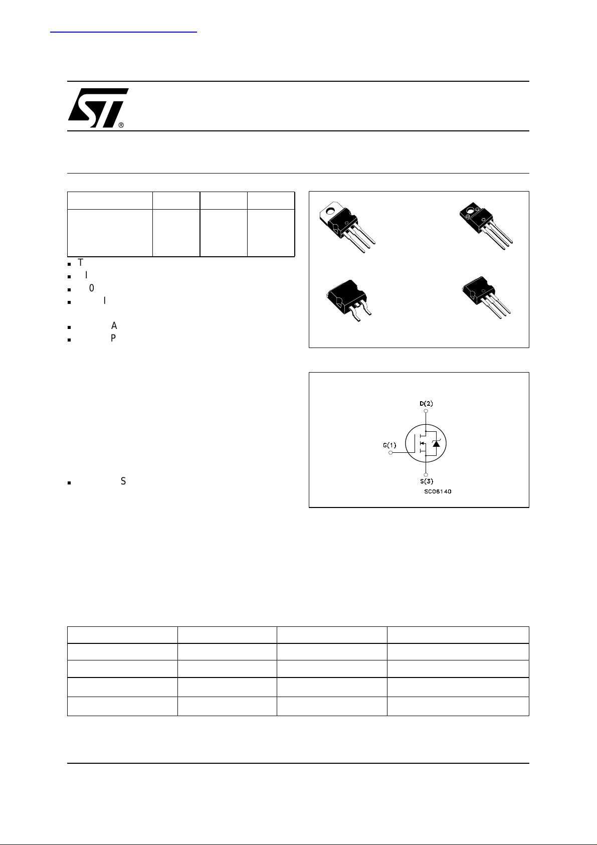
3
2
TO-220
D2PAK
1
3
1
TO-220FP
2
I
INTERNAL SCHEMATIC DIAGRAM
PAK
3
2
1
3
2
1
ORDER CODES
PART NUMBER MARKING PACKAGE PACKAGING
STP11NM60FD P11NM60FD TO-220 TUBE
STP11NM60FDFP P11NM60FDFP TO-220FP TUBE
STB11NM60FDT4 B11NM60FD
STB11NM60FD-1 B11NM60FD
2
PAK
D
2
I
PAK
TAPE & REEL
TUBE
1/13February 2004
Page 2
STP11NM60FD - STP11N M 60FDF P - STB11NM60FD - ST B 11NM60FD -1
ABSOLUTE MAXIMUM RATINGS
Symbol Parameter Value Unit
V
DS
V
DGR
V
GS
I
D
I
D
IDM()
P
TOT
Drain-source Voltage (VGS=0)
Drain-gate Voltage (RGS=20kΩ)
Gate- source Voltage ±30 V
Drain Current (continuos) at TC=25°C
Drain Current (continuos) at TC=100°C
Drain Current (pulsed) 44 44 (*) A
Total Dissipation at TC=25°C
Derating Factor 0.88 0.28 W/°C
1) Peak Diode Recovery voltage slope 20 V/ns
dv/dt (
V
ISO
T
stg
T
j
(•)Pulse width limited by safe operating area
<11A, di/dt<400A/µs, VDD<V
(1)I
SD
(*)Limited only by maximum temperature allowed
Insulation Winthstand Voltage (DC) -- 2500 V
Storage Temperature
Max. Operating Junction Temperature
(BR)DSS,TJ<TJMAX
STP11NM60FD
STB11NM60FD
STB11NM60FD-1
11 11 (*) A
77(*)A
160 35 W
STP11NM60FDFP
600 V
600 V
–65 to 150 °C
THERMAL DATA
TO-220/I
2
PAK
2
PAK
D
Rthj-case Thermal Resistance Junction-case Max 0.78 3.57 °C/W
Rthj-amb Thermal Resistance Junction-ambient Max 62.5 °C/W
T
l
Maximum Lead Temperature For Soldering Purpose 300 °C
TO-220FP
AVALANCHE CHARACTERISTICS
Symbol Parameter Max Value Unit
I
AR
E
AS
Avalanche Current, Repetitive or Not-Repetitive
(pulse width limited by T
max)
j
Single Pulse Avalanche Energy
(starting T
=25°C, ID=IAR,VDD=35V)
j
ELECTRICAL CHARACTERISTICS (T
=25°C UNLESS OTHERWISE SPECIFIED)
CASE
5.5 A
350 mJ
ON/OFF
Symbol Parameter Test Conditions Min. Typ. Max. Unit
V
(BR)DSS
I
DSS
I
GSS
V
GS(th)
R
DS(on)
Drain-source
Breakdown Voltage
Zero Gate Voltage
Drain Current (V
GS
=0)
Gate-body Leakage
Current (V
DS
=0)
Gate Threshold Voltage
Static Drain-source On
Resistance
ID= 250 µA, VGS= 0 600 V
V
=MaxRating
DS
V
=MaxRating,TC= 125 °C
DS
V
=±30V ±100 nA
GS
V
DS=VGS,ID
= 250 µA
34
1µA
100 µA
5V
VGS=10V,ID= 5.5 A 0.40 0.45 Ω
2/13
Page 3

STP11NM60FD - ST P11N M 60F D FP - STB11NM60FD - STB11NM60FD-1
DYNAMIC
Symbol Parameter Test Conditions Min. Typ. Max. Unit
(1) Forward Transconductance VDS>I
g
fs
D(on)xRDS(on)max,
ID=5.5A
C
iss
C
oss
C
rss
Input Capacitance
Output Capacitance 208 pF
Reverse Transfer
V
=25V,f=1MHz,VGS=0
DS
Capacitance
C
oss eq.
(2) Equivalent Output
VGS=0V,VDS= 0V to 400V 100 pF
Capacitance
R
G
Gate Input Resistance f=1 MHz Gate DC Bias = 0
Test Signal Level = 20mV
Open Drain
Note: 1. Pulsed: Pulse duration = 300 µs, duty cycle 1.5 %.
2. C
is defined as a constant equivalent capacitance giving the same charging time as C
oss eq.
.
V
DSS
SWITCHING ON
Symbol Parameter Test Conditions Min. Typ. Max. Unit
t
d(on)
Q
Q
Q
Turn-on Delay Time
t
r
g
gs
gd
Rise Time 16 ns
Total Gate Charge
Gate-Source Charge 7.8 nC
Gate-Drain Charge 13 nC
V
=250V,ID=5.5A
DD
RG=4.7Ω VGS=10V
(see test circuit, Figure 3)
V
=400V,ID=11A,
DD
VGS=10V
5.2 S
1000 pF
28 pF
3 Ω
when VDSincreases from 0 to 80%
oss
20 ns
28 40 nC
SWITCHING OFF
Symbol Parameter Test Conditions Min. Typ. Max. Unit
t
r(Voff)
t
Off-voltage Rise Time
t
f
c
FallTime 15 ns
Cross-over Time 24 ns
V
=400V,ID=11A,
DD
R
=4.7Ω, VGS= 10V
G
(seetest circuit,Figure5)
10 ns
SOURCE DRAIN DIODE
Symbol Parameter Test Conditions Min. Typ. Max. Unit
I
SD
I
SDM
VSD(1)
t
rr
Q
rr
I
RRM
Note: 1. Pulsed: Pulse duration = 300 µs, duty cycle 1.5 %.
2. Pulse width limited by safe operating area.
Source-drain Current 11 A
(2)
Source-drain Current (pulsed) 44 A
ForwardOnVoltage
Reverse Recovery Time
Reverse Recovery Charge 1.1 µC
ISD=11A,VGS=0
= 11A, di/dt = 100A/µs,
I
SD
VDD=50V
(see test circuit, Figure 5)
190 ns
Reverse Recovery Current 14.5 A
1.5 V
3/13
Page 4
STP11NM60FD - STP11N M 60FDF P - STB11NM60FD - ST B 11NM60FD -1
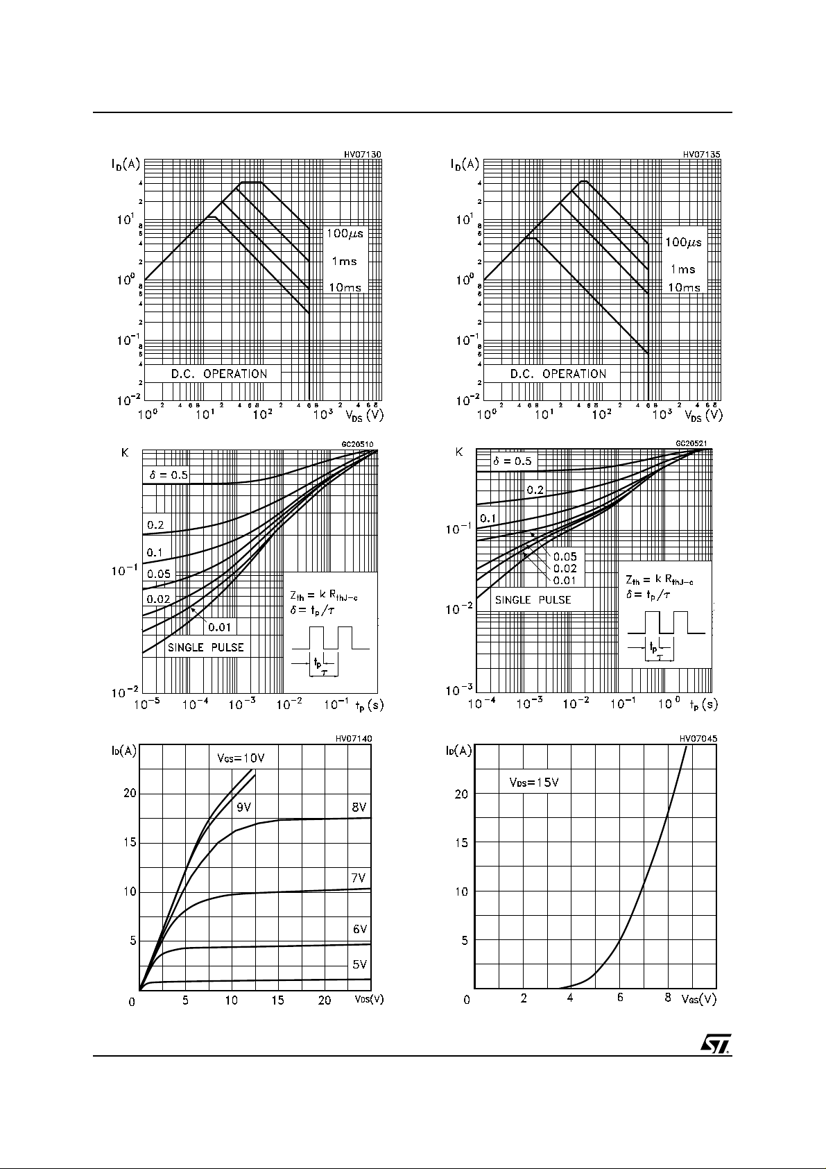
Safe Operating for TO-220/I2PAK/D2PAK Safe Operating Area for TO-220FP
Thermal Impedance for TO-220FPThermal Impedance for TO-220/I2PAK
4/13
Transfer CharacteristicsOutput Characteristics
Page 5

STP11NM60FD - ST P11N M 60F D FP - STB11NM60FD - STB11NM60FD-1
Static Drain-source On ResistanceTransconductance
Gate Charge vs Gate-source Voltage
Capacitance Variations
Normalized On Resistance vs TemperatureNormalized Gate Theresho ld Voltage vs Temp.
5/13
Page 6

STP11NM60FD - STP11N M 60FDF P - STB11NM60FD - ST B 11NM60FD -1
Source-drain Diode Forward Characteristics
6/13
Page 7

STP11NM60FD - ST P11N M 60F D FP - STB11NM60FD - STB11NM60FD-1
Fig. 2: Unclamped Inductive WaveformFig. 1: Unclamped Inductive Load Test Circuit
Fig. 3: Switching Times Test Circuit For
Resistive Load
Fig. 5: Test Circuit For Induc tive Load Switching
And Di ode Recovery T imes
Fig. 4: Gate Charge test Circuit
7/13
Page 8

STP11NM60FD - STP11N M 60FDF P - STB11NM60FD - ST B 11NM60FD -1
TO-220 MECHANICAL DATA
DIM.
A 4.40 4.60 0.173 0.181
b 0.61 0.88 0.024 0.034
b1 1.15 1.70 0.045 0.066
c 0.49 0.70 0.019 0.027
D 15.25 15.75 0.60 0.620
E 10 10.40 0.393 0.409
e 2.40 2.70 0.094 0.106
e1 4.95 5.15 0.194 0.202
F 1.23 1.32 0.048 0.052
H1 6.20 6.60 0.244 0.256
J1 2.40 2.72 0.094 0.107
L 13 14 0.511 0.551
L1 3.50 3.93 0.137 0.154
L20 16.40 0.645
L30 28.90 1.137
øP 3.75 3.85 0.147 0.151
Q 2.65 2.95 0.104 0.116
MIN. TYP MAX. MIN. TYP. MAX.
mm. inch
8/13
Page 9

STP11NM60FD - ST P11N M 60F D FP - STB11NM60FD - STB11NM60FD-1
TO-220FP MECHANICAL DATA
DIM.
A 4.4 4.6 0.173 0.181
B 2.5 2.7 0.098 0.106
D 2.5 2.75 0.098 0.108
E 0.45 0.7 0.017 0.027
F 0.75 1 0.030 0.039
F1 1.15 1.7 0.045 0.067
F2 1.15 1.7 0.045 0.067
G 4.95 5.2 0.195 0.204
G1 2.4 2.7 0.094 0.106
H 10 10.4 0.393 0.409
L2 16 0.630
L3 28.6 30.6 1.126 1.204
L4 9.8 10.6 .0385 0.417
L5 2.9 3.6 0.114 0.141
L6 15.9 16.4 0.626 0.645
L7 9 9.3 0.354 0.366
Ø 3 3.2 0.118 0.126
MIN. TYP MAX. MIN. TYP. MAX.
mm. inch
E
A
D
B
L3
L6
L7
F1
F
G1
H
F2
123
L4
L2
L5
G
9/13
Page 10

STP11NM60FD - STP11N M 60FDF P - STB11NM60FD - ST B 11NM60FD -1
TO-262 (I2PAK) MECHANICAL DATA
DIM.
A 4.40 4.60 0.173 0.181
A1 2.40 2.72 0.094 0.107
b 0.61 0.88 0.024 0.034
b1 1.14 1.70 0.044 0.066
c 0.49 0.70 0.019 0.027
c2 1.23 1.32 0.048 0.052
D 8.95 9.35 0.352 0.368
e 2.40 2.70 0.094 0.106
e1 4.95 5.15 0.194 0.202
E 10 10.40 0.393 0.410
L 13 14 0.511 0.551
L1 3.50 3.93 0.137 0.154
L2 1.27 1.40 0.050 0.055
MIN. TYP MAX. MIN. TYP. MAX.
mm. inch
10/13
Page 11

STP11NM60FD - ST P11N M 60F D FP - STB11NM60FD - STB11NM60FD-1
D2PAK MECHANICAL DATA
DIM.
MIN. TYP MAX. MIN. TYP. MAX.
A 4.4 4.6 0.173 0.181
A1 2.49 2.69 0.098 0.106
A2 0.03 0.23 0.001 0.009
B 0.7 0.93 0.027 0.036
B2 1.14 1.7 0.044 0.067
C 0.45 0.6 0.017 0.023
C2 1.23 1.36 0.048 0.053
D 8.95 9.35 0.352 0.368
D1 8 0.315
E10 10.40.393
E1 8.5 0.334
G 4.88 5.28 0.192 0.208
L 15 15.85 0.590 0.625
L2 1.27 1.4 0.050 0.055
L3 1.4 1.75 0.055 0.068
mm. inch
M 2.4 3.2 0.094 0.126
R0.4 0.015
V2 0º 4º
3
11/13
1
Page 12

STP11NM60FD - STP11N M 60FDF P - STB11NM60FD - ST B 11NM60FD -1
D2PAK FOOTPRINT
TAPE AND REEL SHIPMENT (suffix ”T4”)*
TUBE SHIPMENT (no suffix)*
REEL MECHANICAL DATA
DIM.
A 330 12.992
B 1.5 0.059
C 12.8 13.2 0.504 0.520
D 20.2 0795
G 24.4 26.4 0.960 1.039
N 100 3.937
T 30.4 1.197
mm inch
MIN. MAX. MIN. MAX.
TAPE MECHANICAL DATA
DIM.
A0 10.5 10.7 0.413 0.421
B0 15.7 15 .9 0.618 0.626
D 1.5 1.6 0.059 0.063
D1 1.59 1.61 0.062 0.063
E 1.65 1.85 0.065 0.073
F 11.4 11.6 0.449 0.456
K0 4.8 5.0 0.189 0.197
P0 3.9 4.1 0.153 0.161
P1 11.9 12.1 0.468 0. 476
P2 1.9 2.1 0.075 0.082
R 50 1.574
T 0.25 0.35 0.0098 0.0137
W 23.7 24.3 0.933 0. 956
* on sales ty pe
12/13
mm inch
MIN. MAX. MIN. MAX.
BASE QTY BULK QTY
1000 1000
Page 13

STP11NM60FD - ST P11N M 60F D FP - STB11NM60FD - STB11NM60FD-1
Information furnished is believed to be accurate and reliable. However, STMicroelectronics assumes no responsibility for the
consequences of u se of suc h informat ion n or for any in fring ement of paten ts or oth er ri ghts of th ird part ies whic h may resul t from
its use. No license is granted by implication or otherwise under any patent or patent rights of STMicroelectronics. Specifications
mentioned in this publication are subject to change without notice. This publication supersedes and replaces all information
previously supplied. STMicroelectronics products are not authorized for use as critical components in life support devices or
systems without express written approval of STMicroelectronics.
Australia - Belgium - Brazil - Canada - China - Czech Republic - Finland - France - Germany - Hong Kong - India - Israel - Italy - Japan -
Malaysia - Malta - Morocco - Singapore - Spain - Sweden - Switzerland - United Kingdom - United States.
The ST logo is a registered trademark of STMicroelectronics
All other names are the property of their respective owners
© 2004 STMicroelectronics - All Rights Reserved
STMicroelectronics GROUP OF COMPANIES
http://www.st.com
13/13
 Loading...