

Datasheet ST93C57M6TR, ST93C57M3TR, ST93C57M6013TR, ST93C57M3013TR, ST93C57M1TR Datasheet (SGS-THOMSON Microelectronics)
...Page 1
ST93C56, 56C
ST93C57C
2K (128 x 16 or 256 x 8)SERIALMICROWIREEEPROM
NOT FOR NEW DESIGN
June 1997 1/13
This isinformation on a productstill in productionbutnot recommendedfor new designs.
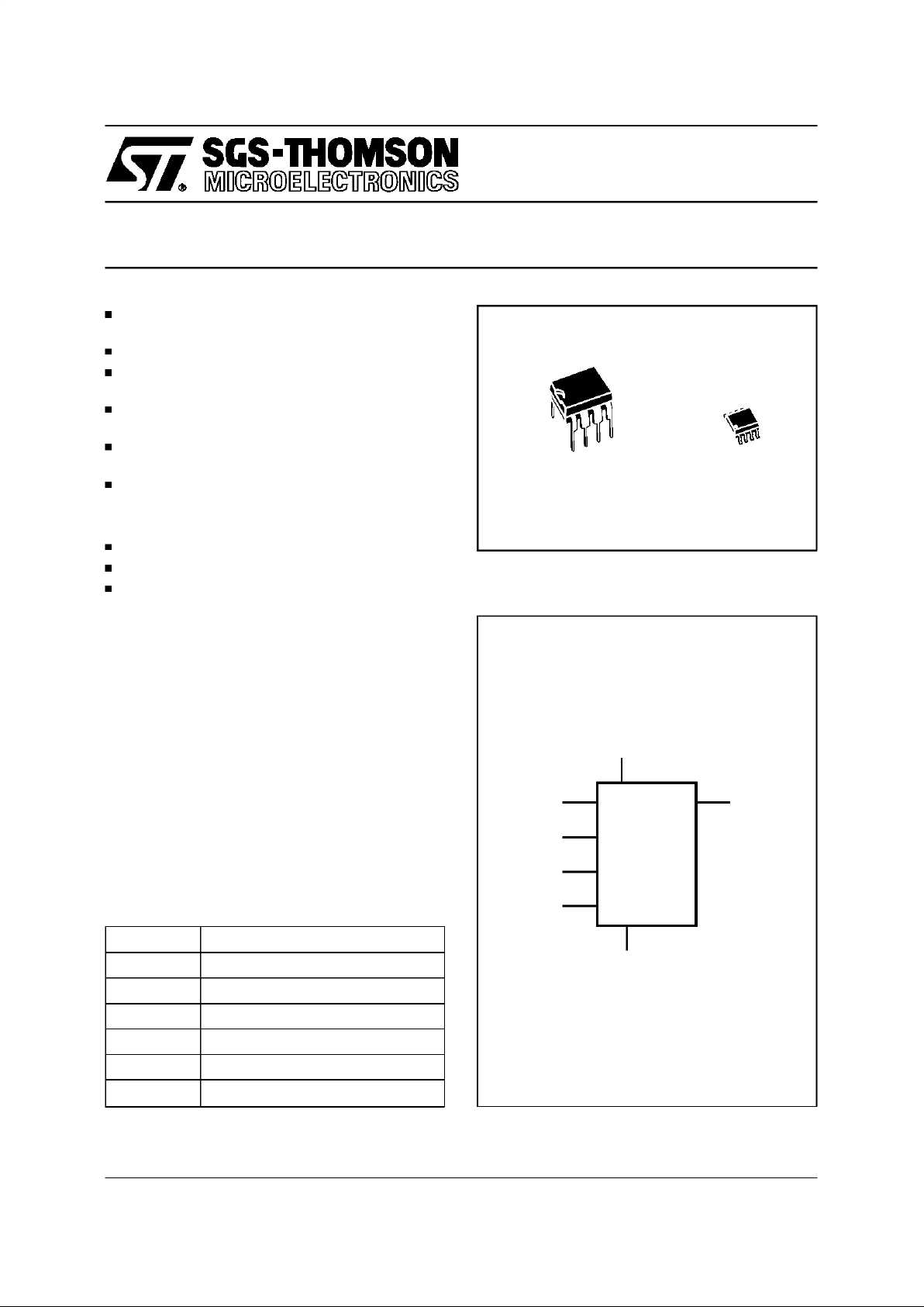
AI00881C
D
V
CC
ST93C56
ST93C57
V
SS
C
Q
S
ORG
Figure 1. Logic Diagram
1 MILLIONERASE/WRITE CYCLES, with
40 YEARS DATARETENTION
DUALORGANIZATION:128 x 16 or 256 x 8
BYTE/WORDand ENTIRE MEMORY
PROGRAMMINGINSTRUCTIONS
SELF-TIMED PROGRAMMINGCYCLE with
AUTO-ERASE
READY/BUSYSIGNALDURING
PROGRAMMING
SINGLESUPPLYVOLTAGE:
– 4.5V to 5.5V for ST93C56version
– 3V to 5.5V for ST93C57 version
SEQUENTIALREAD OPERATION
5ms TYPICALPROGRAMMINGTIME
ST93C56,ST93C56C,ST93C57Care
replacedby the M93C56
DESCRIPTION
This specification covers a range of 2K bit serial
EEPROM products, the ST93C56, 56C specified
at 5V ± 10%and the ST93C57C specified at 3Vto
5.5V. In the text, products are referred to as
ST93C56.
The ST93C56 is a 2K bit Electrically Erasable
ProgrammableMemory(EEPROM)fabricatedwith
SGS-THOMSON’sHighEnduranceSinglePolysilicon CMOS technology. The memory is accessed
through a serial input (D) and output (Q). The 2K
bit memory is divided into either 256 x 8 bit bytes
or 128 x 16 bit words. The organization may be
selectedby a signalappliedon the ORG input.
S Chip Select Input
D Serial Data Input
Q Serial Data Output
C Serial Clock
ORG Organisation Select
V
CC
Supply Voltage
V
SS
Ground
Table 1. Signal Names
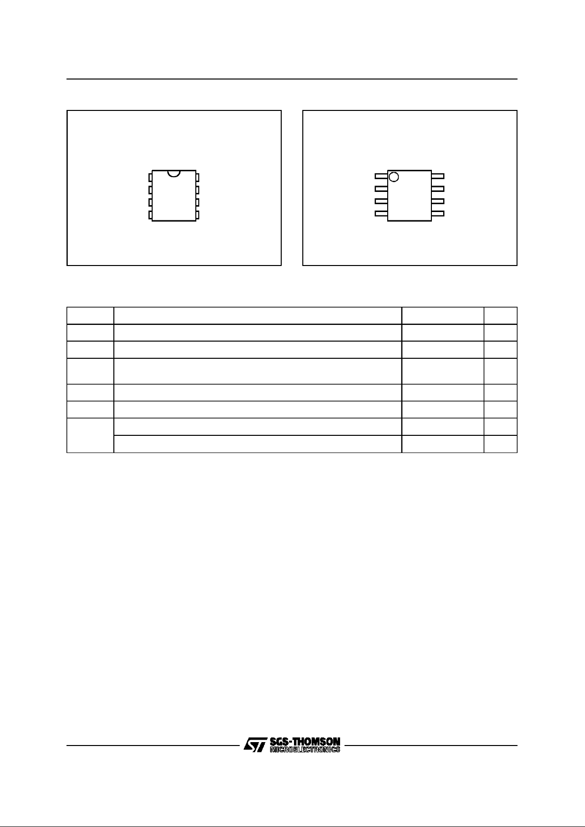
8
1
SO8 (M)
150mil Width
8
1
PSDIP8 (B)
0.4mm Frame
Page 2
The memory is accessed by a set of instructions
which includes Read a byte/word, Write a
byte/word,Erasea byte/word, Erase All and Write
All. AReadinstructionloads theaddressof the first
byte/word to be read into an internal address
pointer. The datacontained at this addressis then
clocked out serially. The address pointer is automaticallyincrementedafter the data is output and,
if the Chip Select input (S) is held High, the
ST93C56 can output a sequential stream of data
bytes/words.In this way,the memorycan be read
as a data stream from 8 to 2048 bits long, or
continuouslyas the addresscounterautomatically
rolls over to ’00’ when the highest address is
reached.Programming is internally self-timed (the
external clock signal on C input may be discon-
nectedorleftrunningafterthestart ofa Writecycle)
and does not require an erase cycle prior to the
Write instruction. The Write instruction writes8 or
16 bits at one time into oneof the256bytesor128
words. After the startof the programming cycle, a
Busy/Readysignal is available on the Data output
(Q)when Chip Select (S) is driven High.
The design of the ST93C56 and the High EnduranceCMOStechnologyusedforitsfabricationgive
an Erase/Write cycle Enduranceof 1,000,000cyclesand a data retention of 40 years.
TheDU (Don’tUse) pindoes notaffectthefunction
of the memory and it is reserved for use by SGSTHOMSON duringtestsequences.Thepinmaybe
left unconnectedor may be connected to V
CC
or
V
SS
. Direct connection of DU to VSSis recommended for the lowest standby power consumption.
V
SS
Q
ORG
DUC
SV
CC
D
AI00882C
ST93C56
ST93C57
1
2
3
4
8
7
6
5
Figure2A. DIPPin Connections
1
V
SS
Q
ORG
DUC
SV
CC
D
AI00883D
ST93C56
ST93C57
2
3
4
8
7
6
5
Figure2B. SO Pin Connections
DESCRIPTION (cont’d)
Warning: DU = Don’t Use Warning: DU = Don’t Use
Symbol Parameter Value Unit
T
A
Ambient Operating Temperature –40 to125 °C
T
STG
Storage Temperature –65 to150 °C
T
LEAD
Lead Temperature,Soldering (SO8 package)
(PSDIP8 package)
40 sec
10 sec
215
260
°C
V
IO
Input or Output Voltages(Q = VOHor Hi-Z) –0.3 to VCC+0.5 V
V
CC
Supply Voltage –0.3 to 6.5 V
V
ESD
Electrostatic Discharge Voltage (Human Body model)
(2)
4000 V
Electrostatic Discharge Voltage (Machine model)
(3)
500 V
Notes: 1. Exceptfor the rating ”Operating Temperature Range”, stresses above those listed in the Table ”Absolute Maximum Ratings”
may cause permanent damage to thedevice. These are stress ratings only and operation of the device at these or any other
conditions abovethose indicated in the Operating sections of this specification is not implied. Exposure toAbsolute Maximum
Rating conditions for extended periods may affect device reliability.Refer also to the SGS-THOMSON SURE Program and other
relevant quality documents.
2. MIL-STD-883C, 3015.7(100pF, 1500 Ω).
3. EIAJ IC-121 (Condition C) (200pF, 0 Ω).
Table 2. Absolute MaximumRatings
(1)
2/13
ST93C56/56C, ST93C57C
Page 3
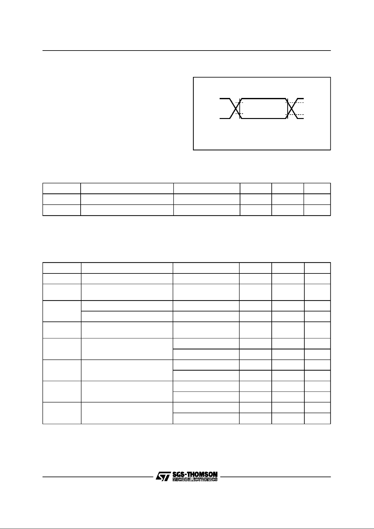
Input Rise and Fall Times ≤ 20ns
Input Pulse Voltages 0.4V to 2.4V
Input Timing Reference Voltages 1V to 2.0V
Output Timing Reference Voltages 0.8V to 2.0V
AC MEASUREMENT CONDITIONS
Note that Output Hi-Z is defined as the point where data
is no longer driven.
AI00815
2.4V
0.4V
2.0V
0.8V
2V
1V
INPUT OUTPUT
Figure 3. ACTesting Input Output Waveforms
Symbol Parameter Test Condition Min Max Unit
C
IN
Input Capacitance VIN=0V 5 pF
C
OUT
Output Capacitance V
OUT
=0V 5 pF
Note: 1. Sampled only, not 100% tested.
Table 3. Capacitance
(1)
(TA=25°C, f =1 MHz )
Symbol Parameter TestCondition Min Max Unit
I
LI
Input Leakage Current 0V ≤ VIN≤ V
CC
±2.5 µA
I
LO
Output Leakage Current
0V ≤ V
OUT
≤ VCC,
Q inHi-Z
±2.5 µA
I
CC
Supply Current (TTL Inputs) S = VIH, f = 1 MHz 3 mA
Supply Current (CMOS Inputs) S = V
IH
, f = 1 MHz 2 mA
I
CC1
Supply Current (Standby)
S=V
SS
,C=VSS,
ORG = V
SS
or V
CC
50 µA
V
IL
Input Low Voltage (D, C, S)
V
CC
=5V±10% –0.3 0.8 V
3V ≤ V
CC
≤ 4.5V –0.3 0.2V
CC
V
V
IH
Input High Voltage (D, C, S)
V
CC
=5V±10% 2 VCC+1 V
3V ≤ V
CC
≤ 4.5V 0.8 V
CC
VCC+1 V
V
OL
Output Low Voltage
I
OL
= 2.1mA 0.4 V
I
OL
=10µA 0.2 V
V
OH
Output High Voltage
I
OH
= –400µA 2.4 V
I
OH
= –10µAV
CC
–0.2 V
Table 4. DC Characteristics
(T
A
= 0 to70°C or –40 to 85°C; VCC= 4.5V to 5.5V or 3V to 5.5V)
3/13
ST93C56/56C, ST93C57C
Page 4
Symbol Alt Parameter Test Condition Min Max Unit
t
SHCH
t
CSS
Chip Select High to Clock High 50 ns
t
CLSH
t
SKS
Clock Low to Chip Select High 100 ns
t
DVCH
t
DIS
Input Valid to Clock High 100 ns
t
CHDX
t
DIH
Clock High to Input Transition
Temp.Range: grade 1 100 ns
Temp.Range:
grades 3, 6
200 ns
t
CHQL
t
PD0
Clock High to Output Low 500 ns
t
CHQV
t
PD1
Clock High to Output Valid 500 ns
t
CLSL
t
CSH
Clock Low to Chip Select Low 0 ns
t
SLCH
Chip Select Low to ClockHigh 250 ns
t
SLSH
t
CS
Chip Select Low to Chip Select High Note 1 250 ns
t
SHQV
t
SV
Chip Select High to Output Valid 500 ns
t
SLQZ
t
DF
Chip Select Low to Output Hi-Z
ST93C56 300 ns
ST93C56C, 57C 200 ns
t
CHCL
t
SKH
Clock High to Clock Low Note 2 250 ns
t
CLCH
t
SKL
Clock Low to Clock High Note 2 250 ns
t
W
t
WP
Erase/Write Cycle time 10 ms
f
C
f
SK
Clock Frequency 0 1 MHz
Notes: 1. Chip Select must bebrought low for a minimum of 250 ns(t
SLSH
) betweenconsecutive instructioncycles.
2. The Clock frequency specification calls for aminimum clock period of 1 µs, therefore the sum of the timings t
CHCL+tCLCH
must be greater or equal to 1 µs. For example, ift
CHCL
is 250 ns, then t
CLCH
must be at least 750ns.
Table 5. AC Characteristics
(T
A
= 0 to70°C or –40 to 85°C; VCC= 4.5V to 5.5V or 3V to 5.5V)
AI01428
C
OP CODE OP CODESTART
S
D
OP CODE INPUTSTART
tDVCH
tSHCH
tCLSH tCHCL
tCLCH
tCHDX
Figure4. Synchronous Timing, Start and Op-CodeInput
4/13
ST93C56/56C, ST93C57C
Page 5

Figure5. Synchronous Timing,Read or Write
AI00820C
C
D
Q
ADDRESS INPUT
Hi-Z
tDVCH
tCLSL
A0
S
DATA OUTPUT
tCHQVtCHDX
tCHQL
An
tSLSH
tSLQZ
Q15/Q7 Q0
AI01429
C
D
Q
ADDRESS/DATA INPUT
Hi-Z
tDVCH
tSLCH
A0/D0
S
WRITE CYCLE
tSLSHtCHDX
An
tCLSL
tSLQZ
BUSY
tSHQV
tW
READY
MEMORY ORGANIZATION
The ST93C56 is organized as 256bytes x8 bitsor
128 wordsx 16 bits. If theORGinput isleft unconnected(or connected to V
CC
) the x16 organization
is selected, when ORG is connected to Ground
(V
SS
) the x8 organization is selected. When the
ST93C56 is in standby mode, the ORG input
should be unconnectedor set to eitherV
SS
or V
CC
in order to achievethe minimumpower consumption. Any voltagebetween V
SS
and VCCapplied to
ORG may increase the standby current value.
POWER-ONDATA PROTECTION
In orderto prevent data corruption and inadvertent
write operations during power up, a Power On
Reset(POR)circuitresetsall internalprogramming
circuitry and sets the device in the Write Disable
mode. WhenV
CC
reachesits functionalvalue,the
deviceisproperlyreset(intheWrite Disablemode)
and is ready to decode and execute an incoming
instruction. A stable V
CC
must be applied, before
applyingany logic signal.
5/13
ST93C56/56C, ST93C57C
Page 6

Instruction
Description Op-Code
x8 Org
Address
(ORG = 0)
(1, 2)
Data
x16 Org
Address
(ORG = 1)
(1, 3)
Data
READ Read Data from Memory 10 A8-A0 Q7-Q0 A7-A0 Q15-Q0
WRITE Write Data to Memory 01 A8-A0 D7-D0 A7-A0 D15-D0
EWEN Erase/Write Enable 00 11XXX XXXX 11XX XXXX
EWDS Erase/Write Disable 00 00XXX XXXX 00XX XXXX
ERASE Erase Byte or Word 11 A8-A0 A7-A0
ERAL Erase All Memory 00 10XXX XXXX 10XX XXXX
WRAL
Write All Memory
with same Data
00 01XXX XXXX D7-D0 01XX XXXX D15-D0
Notes: 1. X = don’t care bit.
2. Address bit A8 is not decoded by the ST93C56, ST93C56C.
3. Address bit A7 is not decoded by the ST93C56, ST93C56C.
Table 6. InstructionSet
INSTRUCTIONS
The ST93C56 has seveninstructions,asshownin
Table 6. The op-codes ofthe instructionsare made
up of 2 bits.Theop-codeisfollowedbyanaddress
for the byte/wordwhichis eightbitslongforthex16
organization or nine bits long for the x8 organization.Eachinstructionisprecededbytherising edge
of the signal applied on the Chip Select (S) input
(assumingthat the clock C is low). The datainput
D is thensampled upon the following rising edges
of the clock C untill a ’1’ is sampled and decoded
by the ST93C56 as a Start bit.
The ST93C56 is fabricated in CMOS technology
and is therefore able to run from zero Hz (static
inputsignals)up to themaximumratings(specified
in Table 5).
Read
The Read instruction (READ) outputs serial data
on the Data Output (Q). When a READ instruction
is received, the instruction and address are decodedandthe datafromthememoryis transferred
intoanoutputshiftregister.Adummy’0’bitisoutput
first, followed by the 8 bit byte or the 16 bit word
with the MSB first. Output data changes are triggeredby theLowtoHightransitionoftheClock(C).
The ST93C56 will automaticallyincrement the addressand will clock out the next byte/wordas long
as the Chip Select input (S) is held High. In this
case the dummy ’0’ bit is NOT output between
bytes/wordsand a continuousstream of data can
be read.
Erase/WriteEnable and Disable
The Erase/Write Enable instruction (EWEN)
authorizesthe followingErase/Writeinstructionsto
be executed, the Erase/Write Disable instruction
(EWDS) disables the execution of the following
Erase/Write instructions. When power is first applied, the ST93C56 enters the Disable mode.
When the EWEN instruction is executed, Write
instructions remain enabled until an Erase/Write
Disableinstruction(EWDS) is executedorV
CC
falls
belowthe power-onreset threshold.To protect the
memory contents from accidental corruption, it is
advisableto issuetheEWDSinstructionafterevery
write cycle.
The READinstructionis notaffected by theEWEN
or EWDSinstructions.
Erase
The Eraseinstruction (ERASE) programs the addressedmemory byte or word bits to ’1’. Once the
addressiscorrectlydecoded,the fallingedgeof the
Chip Select input (S) triggers a self-timed erase
cycle.
If the ST93C56 is still performing the erasecycle,
the Busysignal(Q =0) will bereturnedif Sisdriven
high, andthe ST93C56will ignore any data on the
bus. Whentheerasecycleiscompleted,theReady
signal (Q = 1) will indicate (if S is drivenhigh) that
the ST93C56is ready to receive a new instruction.
Write
The Write instruction (WRITE) is followed by the
addressandthe8or16 databitstobewritten.Data
input is sampled on the Low to High transition of
the clock.After thelast data bit hasbeensampled,
Chip Select (S) must be brought Low before the
next rising edge of the clock (C) in order to start
the self-timedprogramming cycle. If the ST93C56
is still performing the write cycle, the Busy signal
6/13
ST93C56/56C, ST93C57C
Page 7

AI00878C
110An A0
Qn Q0
DATA OUT
D
S
Q
READ
SWRITE
ADDR
OP
CODE
1 0 An A0
DATA IN
D
Q
OP
CODE
Dn D01
BUSY READY
S
ERASE
WRITE
ENABLE
1 0 Xn X0D
OP
CODE
101
S
ERASE
WRITE
DISABLE
1 0 Xn X0D
OP
CODE
000
CHECK
STATUS
ADDR
Figure6. READ, WRITE, EWEN, EWDS Sequences
(Q = 0) will bereturned if S is driven high, and the
ST93C56willignoreanydataon thebus.Whenthe
writecycle is completed, the Ready signal(Q = 1)
will indicate(if S is drivenhigh) that the ST93C56
isreadyto receiveanewinstruction.Programming
is internallyself-timed (the externalclocksignalon
C input may be disconnectedor left running after
the start of a programming cycle) and does not
require an Erase instruction prior to the Write instruction (The Write instruction includes an automatic erase cycle before programingdata).
Notes: 1. An: n = 7 for x16 org.and 8 for x8 org.
2. Xn: n = 5 for x16 org. and 6 for x8 org.
7/13
ST93C56/56C, ST93C57C
Page 8

AI00879B
SERASE
11D
Q
ADDR
OP
CODE
1
BUSY READY
CHECK
STATUS
S
ERASE
ALL
10D
Q
OP
CODE
1
BUSY READY
CHECK
STATUS
00
An A0
Xn X0
ADDR
Figure7. ERASE, ERAL Sequences
AI00880C
SWRITE
ALL
DATA IN
D
Q
ADDR
OP
CODE
Dn D0
BUSY READY
CHECK
STATUS
1000 1 Xn X0
Figure8. WRAL Sequence
Notes: 1. An:n = 7 forx16 org. and 8 for x8 org.
2. Xn: n = 5 for x16 org. and 6 for x8org.
Note: 1. Xn: n = 5 for x16 org. and 6 for x8 org.
8/13
ST93C56/56C, ST93C57C
Page 9

Erase All
The Erase All instruction(ERAL) erasesthe whole
memory (all memory bits are set to ’1’). A dummy
addressis input duringthe instructiontransfer and
the erase is made in the sameway as the ERASE
instruction. If the ST93C56 is still performing the
erasecycle,theBusysignal(Q=0) willbe returned
if S is driven high,and the ST93C56will ignore any
data on the bus. When the erase cycle is completed, the Ready signal (Q = 1) will indicate (if S
isdrivenhigh)that theST93C56is readyto receive
a new instruction.
WriteAll
The Write All instruction (WRAL) writes the Data
Input byte or word to all the addresses of the
memory. If theST93C56is stillperformingthe write
cycle, the Busy signal (Q = 0) will be returnedif S
is driven high, and the ST93C56 will ignore any
dataon the bus.Whenthewritecycle iscompleted,
the Ready signal(Q = 1) willindicate (if S is driven
high) that the ST93C56is ready to receive a new
instruction.
READY/BUSY Status
During every programming cycle (after a WRITE,
ERASE, WRALor ERALinstruction) the DataOutput (Q) indicates the Ready/Busy status of the
memory when the Chip Select (S) is driven High.
Once the ST93C56 is Ready, the Ready/Busy
status is available on the Data Output (Q) until a
new start bit is decoded or the Chip Select (S) is
broughtLow.
COMMONI/O OPERATION
TheData Output(Q)andDataInput(D)signalscan
be connected together, through a current limiting
resistor, to form a common, one wire data bus.
Some precautionsmust be taken when operating
the memorywith thisconnection,mostlytoprevent
a shortcircuit betweenthe last entered addressbit
(A0) and the firstdata bit output by Q. The reader
may also refer to the SGS-THOMSONapplication
note”MICROWIREEEPROMCommonI/OOperation”.
DIFFERENCES BETWEEN ST93C56 AND
ST93C56C
The ST93C56C is an enhanced version of the
ST93C56 and offers a functional security filtering
glitcheson the clockinput (C).
The followingdescription willdetailthe Clock pulse
counter(available only on the ST93C56C).
In a normal environment,the ST93C56expects to
receive the exact amount of data on the D input,
that is, the exact amount of clock pulses on the C
input.
In a noisy environment,the number of pulses received (on the clockinput C) may be greater than
the clockpulsesdeliveredby theMaster(Microcontroller) driving the ST93C56C. In such a case, a
part of the instruction is delayed by one bit (see
Figure 9), and it may induce an erroneouswrite of
data at a wrongaddress.
The ST93C56C has an on-chip counter which
counts the clockpulses from the Startbit until the
falling edge of the Chip Select signal. For the
WRITE instructions, the number of clock pulses
incoming to the counter must be exactly 20 (with
the Organisation by 8) from the Start bit to the
fallingedgeofChip Selectsignal(1 Startbit+2bits
of Op-code+ 9 bits of Address + 8 bits of Data =
20): if so, the ST93C56C executes the WRITE
instruction; if the number of clock pulses is not
equal to 20, the instruction will not be executed
(and data will not be corrupted).
In the same way, when the Organisationby 16 is
selected, the number of clock pulses incoming to
the countermust be exactly27 (1 Startbit + 2 bits
of Op-code+ 8 bits of Address + 16 bits of Data =
27) from the Start bit to the falling edge of Chip
Select signal: if so, the ST93C56C executes the
WRITEinstruction;if thenumberof clockpulsesis
not equal to27, theinstructionwillnot be executed
(and data will not be corrupted). The clock pulse
counter is active only on ERASE and WRITE instructions(WRITE, ERASE,ERAL,WRALL).
9/13
ST93C56/56C, ST93C57C
Page 10

ORDERING INFORMATION SCHEME
AI01395
S
An-1
C
D
WRITE
START D0”1””0”
An
Glitch
An-2
ADDRESS AND
DATA
ARE SHIFTED BY ONE BIT
Figure9. WRITE Sequence with One Clock Glitch
Operating Voltage
56 4.5V to 5.5V
57 3V to 5.5V
Revision
blank CMOS F3
C CMOS F4
Package
B PSDIP8
0.4 mm Frame
M SO8
150mil Width
Temperature Range
1 0 to 70 °C
6 –40 to 85 °C
3
(1)
–40 to 125 °C
Option
013TR Tape& Reel
Packing
(A, T ver.)
TR Tape& Reel
Packing
(C version)
Example: ST93C56C M 1 013TR
Note: 1. Temperature range on special request only.
Devicesare shipped from the factory with the memorycontentset at all ”1’s” (FFFFh for x16, FFh for x8).
For a list of availableoptions (Operating Voltage,Package, etc...) or for further information on any aspect
of thisdevice, please contact theSGS-THOMSON Sales Office nearestto you.
10/13
ST93C56/56C, ST93C57C
Page 11

PSDIP-a
A2A1A
L
e1
D
E1 E
N
1
C
eA
eB
B1
B
Symb
mm inches
Typ Min Max Typ Min Max
A 4.80 0.189
A1 0.70 – 0.028 –
A2 3.10 3.60 0.122 0.142
B 0.38 0.58 0.015 0.023
B1 1.15 1.65 0.045 0.065
C 0.38 0.52 0.015 0.020
D 9.20 9.90 0.362 0.390
E 7.62 – – 0.300 – –
E1 6.30 7.10 0.248 0.280
e1 2.54 – – 0.100 – –
eA 8.40 – 0.331 –
eB 9.20 0.362
L 3.00 3.80 0.118 0.150
N8 8
CP 0.10 0.004
PSDIP8
Drawing is not to scale
PSDIP8 - 8 pin Plastic Skinny DIP, 0.4mm lead frame
11/13
ST93C56/56C, ST93C57C
Page 12

SO-a
E
N
CP
B
e
A
D
C
LA1 α
1
H
hx45°
Symb
mm inches
Typ Min Max Typ Min Max
A 1.35 1.75 0.053 0.069
A1 0.10 0.25 0.004 0.010
B 0.33 0.51 0.013 0.020
C 0.19 0.25 0.007 0.010
D 4.80 5.00 0.189 0.197
E 3.80 4.00 0.150 0.157
e 1.27 – – 0.050 – –
H 5.80 6.20 0.228 0.244
h 0.25 0.50 0.010 0.020
L 0.40 0.90 0.016 0.035
α 0° 8° 0° 8°
N8 8
CP 0.10 0.004
SO8
Drawing is not to scale
SO8 - 8 lead Plastic Small Outline, 150 mils body width
12/13
ST93C56/56C, ST93C57C
Page 13

Information furnished is believed to be accurate and reliable.However, SGS-THOMSON Microelectronics assumes no responsibility for the
consequences of use of such information nor for any infringementof patents or other rights of third parties which may result from its use.No
license is granted by implication or otherwise under any patentor patent rights ofSGS-THOMSON Microelectronics. Specificationsmentioned
in this publication are subject to change without notice. This publication supersedes and replaces all information previously supplied.
SGS-THOMSON Microelectronics productsare notauthorized foruse ascritical components in life supportdevices or systemswithout express
written approval of SGS-THOMSONMicroelectronics.
1997 SGS-THOMSON Microelectronics - All Rights Reserved
MICROWIRE isa registered trademark of National SemiconductorCorp.
SGS-THOMSON Microelectronics GROUP OF COMPANIES
Australia - Brazil - Canada- China - France - Germany - Hong Kong - Italy - Japan - Korea- Malaysia - Malta - Morocco - The Netherlands -
Singapore- Spain - Sweden - Switzerland - Taiwan- Thailand - United Kingdom - U.S.A.
13/13
ST93C56/56C, ST93C57C
 Loading...