

Page 1
®
HIGH VOLTAGE FAST-SWITCHING
■ MEDIUM VOLTAGE CAPABILITY
■ LOW SPREAD OF DYNAMIC PARAMETERS
■ MINIMUM LOT- TO- LO T SPR E AD FO R
RELIABLE OPERATION
■ VERY HIGH SWI TCHING SPEED
APPLICATIONS:
■ ELECTRONIC BALLASTS FOR
FLUORESCENT LIGHTING
DESCRIPTION
The device is manufactured using high voltage
Multi-Epitaxial Planar technology for high
switching speeds and medium voltage capability.
It uses a Cellular Emitter structure with planar
edge termination to enhance switching speeds
while maintaining the wide RBSOA.
The ST93003 is expressly designed for a new
solution to be used in compact fluorescent lamps,
where it is coupled with the ST83003, its
complementary NPN tra nsist or.
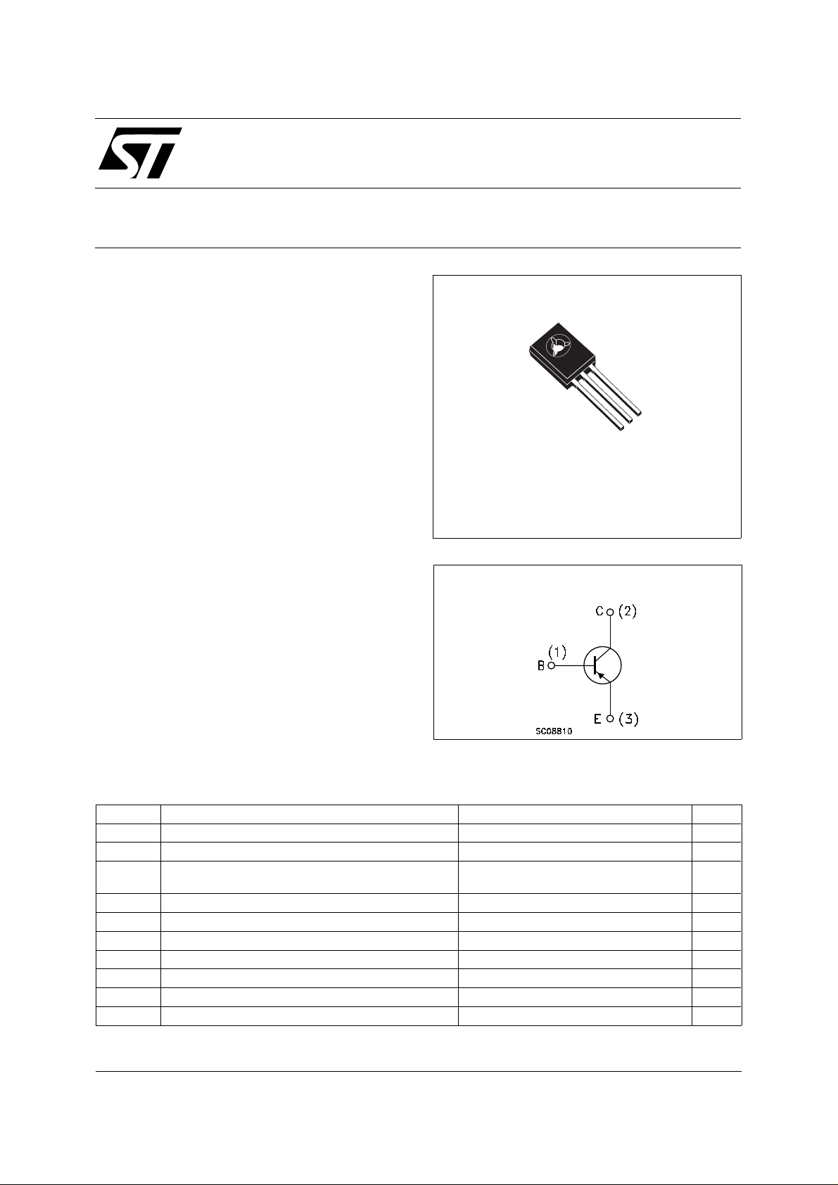
ST93003
PNP POWER TRANSISTOR
1
2
3
SOT-32
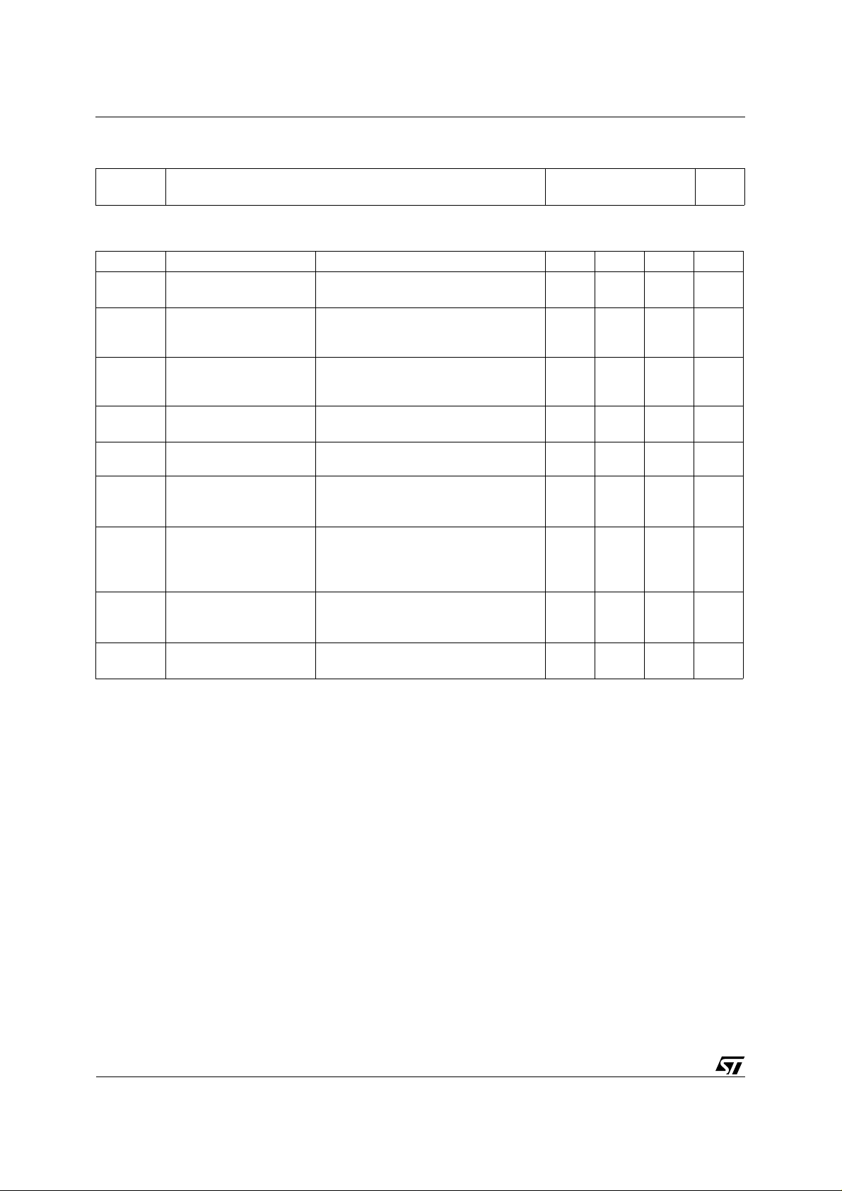
INTERNAL SCHEMATIC DIAGRAM
ABSOL UT E MAXIMU M RATINGS
Symbol Parameter Value Unit
V
V
V
I
I
P
T
October 2002
Collector-Emitter Voltage (VBE = 0) -500 V
CES
Collector-Emitter Voltage (IB = 0) -400 V
CEO
Emitter-Base Voltage
EBO
= 0, IB = -0.75 A, tp < 10µs, Tj < 150oC)
(I
C
I
Collector Current -1.5 A
C
Collector Peak Current (tp < 5 ms) -3 A
CM
Base Current -0.75 A
I
B
Base Peak Current (tp < 5 ms) -1.5 A
BM
Total Dissipation at Tc = 25 oC40W
tot
Storage Temperature -65 to 150
stg
Max. Operating Junction Temperature 150
T
j
V
(BR)EBO
V
o
C
o
C
1/7
Page 2
ST93003
THERMAL DATA
R
thj-case
R
thj-amb
Thermal Resistance Junction-case Max
Thermal Resistance Junction-ambient Max
3.12
89
o
C/W
o
C/W
ELECTRICAL CHARACTERISTICS (T
= 25 oC unless otherwise specified)
case
Symbol Parameter Test Conditions Min. Typ. Max. Unit
I
CES
V
(BR)EBO
Collector Cut-off
Current (V
BE
= 0)
Emitter Base
= -500V
V
CE
V
= -500V T
CE
I
= -10 mA -5 -10 V
E
= 125oC
j
-1
-5
Breakdown Voltage
(I
= 0)
C
V
CEO(sus)
V
CE(sat)
V
BE(sat)
∗ Collector-Emitter
Sustaining Voltage
(I
= 0)
B
∗ Collector-Emitter
Saturation Voltage
∗ Base-Emitter
I
= -10 mA
C
-400 V
L = 25 mH
IC = -0.5 A IB = -0.1 A
I
= -0.35 A IB = -50 mA
C
-0.5
-0.5
IC = -0.5 A IB = -0.1 A -1 V
Saturation Voltage
∗ DC Current Gain IC = -10 mA V
h
FE
I
= -0.35 A V
C
I
= -1 A V
C
CE
CE
CE
= -5 V
= -5 V
= -5 V
10
16
25 32
4
RESISTIVE LOAD
t
Rise Time
r
s
t
f
Storage Time
Fall Time
t
INDUCTIVE LOAD
t
E
∗ Pulsed: Pulse duration = 300µs, duty cycle = 1.5 %
Storage Time
s
Fall Time
t
f
Avalanche Energy L = 4 mH C = 1.8 nF
sb
I
= -0.35 A VCC = 125 V
C
I
= -70 mA IB2 = 70 mA
B1
≥ 25 µs (see Figure 2)
T
p
I
= -0.5 A IB1 = -0.1 A
C
V
= 5 V L = 10 mH
BE(off)
V
= 300 V (see Figure 1)
clamp
≤ 2.5 A 25oC < TC < 125oC
I
BR
90
1.5
2.2
2.9
0.1
400
40
12 mJ
mA
mA
V
V
ns
µs
µs
ns
ns
2/7
Page 3
ST93003
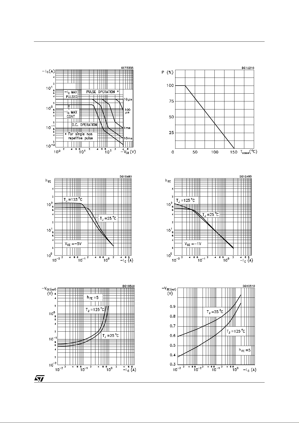
Safe Operating Are a
DC Current Gain
Derating Curve
DC Current Gain
Collector Emitter Sat uration Volt a ge
Base Emitter Satur ation Voltage
3/7
Page 4

ST93003
Resistive Fall Ti me Resistive Storage Time
Inductive Fall Time Inductive Storage Time
Reverse B iased SOA
4/7
Page 5

Figure 1: Inductive Load Switching Test Circuit.
1) Fast electronic switch
2) Non-inductive Resistor
3) Fast recovery rectifier
Figure 2: Resistive Load Switching Test Circuit.
ST93003
1) Fast electronic switch
2) Non-inductive Resistor
5/7
Page 6

1: Base
2: Collector
3: Emitter
ST93003
SOT- 32 (TO-12 6) MECHAN ICAL DATA
DIM.
MIN. TYP. MAX. MIN. TYP. MAX.
A 7.4 7.8 0.291 0.307
B 10.5 10.8 0.413 0.425
b 0.7 0.9 0.028 0.035
b1 0.40 0.65 0.015 0.025
C 2.4 2.7 0.094 0.106
c1 1.0 1.3 0.039 0.051
D 15.4 16.0 0.606 0.630
e 2.2 0.087
e3 4.4 0.173
F 3.8 0.150
G 3 3.2 0.118 0.126
H 2.54 0.100
H2 2.15 0.084
I 1.27 0.05
O 0.3 0.011
V10
mm inch
o
10
o
0016114/B
6/7
Page 7
ST93003
Information furnished is believed to be accurate and reliable. However, STMicroelectronics assumes no responsibility for the consequences
of use of such inform ation nor for any infringe ment o f patents or other rig hts o f third par ties which ma y resul t from i ts use. N o li cen se is
granted by implicatio n or otherwise under any patent or patent rights of STMicroelectronics. Specification mentioned in this publication are
subject to change without notice. This publication supersedes and replaces all information previously supplied. STMicroelectronics products
are not authorized for use as critical compo nents in life support devices or systems without express written approval of STMicroelectronics.
The ST logo is a trademark of STMicroelectronics
© 2002 STMicroelectro nics – Printed in Italy – All Rights Reserved
STMicroelectronics GROUP OF COMPANIES
Australia - Brazil - Canada - China - Finland - France - Germany - Hong Kong - India - Israel - Italy - Japan - Malaysia - Malta - Morocco -
Singapore - Spain - Sweden - Switzerland - United Kingdom - United States.
http://www.st.com
7/7
 Loading...