

Datasheet ST92T163R4T1V, ST92T163R4T1L, ST92T163R4T1E, ST92T163R4T1, ST92T163N4B1E Datasheet (SGS Thomson Microelectronics)
...Page 1

January 2000 1/224
This ispreliminary information on a newproductin developmentorundergoing evaluation. Details are subject tochangewithout notice.
ST92163
8/16-BIT FULL SPEED USB MCU FOR COMPOSITE DEVICES
WITH 16 ENDPOINTS, 20K ROM, 2K RAM, I2C, SCI, & MFT
PRELIMINARY DATA
■ Internal Memories: 20 Kbytes ROM/EPROM/
OTP, 2 Kbytes RAM
■ Register oriented 8/16 bit core
■ 224 general purpose registers available as
RAM, accumulators or index pointers
■ Minimum instruction cycle time: 167 ns (@24
MHz CPU frequency)
■ Low power modes: WFI, SLOW, HALT and
STOP
■ DMA controller for reduced processor overhead
■ Full speed USB interface with DMA, compliant
with USB specifications version 1.1 (in normal
voltage mode)
■ USB Embedded Functions with 16 fully
configurable endpoints (buffer size
programmable), supporting all USB data
transfer types (Isochronous included)
■ On-chip USB transceiver and 3.3 voltage
regulator
■ Multimaster I
2
C-bus serial interface up to
400KHz. with DMA capability
■ Serial Communications Interface (SCI) with
DMA capability:
– Asynchronous mode up to 315 Kb/s
– Synchronous mode up to 3 MHz
■ External memory interface (8-bit data/16-bit
address) with DMA capability from the USB
■ 16-bit Multi-Function Timer (12 operating
modes) with DMA capability
■ 16-bit Timer with 8-bit prescaler and Watchdog
■ 6-channel, 8-bit A/D Converter (ADC)
■ 15 interrupt pins on 8 interrupt channels
■ 14 pins programmable as wake-up oradditional
external interrupts
■ 42 (DIP56) or 44 (QFP64) fully programmable
I/Os with 6 or 8 high sink pads (10 mA @ 1 V)
■ Programmable PLL clock generator (RCCU)
using a low frequency external quartz (8 MHz)
■ On-chip RC oscillator for low power operation
■ Low Voltage Detector Reset on some devices
1
■ Rich instructionset with 14 addressing modes
■ Several operating voltage modes available on
some devices1:
– Normal Voltage Mode
– 8-MHz Low Voltage Mode
– 16-MHz Low Voltage Mode
■ 0 -24 MHzCPU clockoperation @4.0-5.5 V(all
devices)
■ 0 - 8 MHz CPU clock operation @ 3.0-4.0 V (8-
MHz and 16-MHz Low Voltage devices)
■ 0 - 16 MHz CPU clock operation @ 3.0-4.0 V
(16-MHz Low Voltage devices only)
■ Division-by-zero trap generation
■ 0
o
Cto70oC temperature range
■ Low EMI design supporting single sided PCB
■ Complete development tools, including
assembler, linker, C-compiler, archiver, source
level debugger and hardware emulators, and
Real Time Operating System
Note 1: Refer to “DeviceSummary” onpage 6
1
TQFP64
PSDIP56
Rev. 1.9
Page 2

2/224
Table of Contents
ST92163 ............................................1
1 GENERAL DESCRIPTION . . . . . . ................................................ 6
1.1 INTRODUCTION . . . . . . . . . . . . ............................................. 6
1.1.1 Core Architecture . . . . . . . . . . . . . . . . . .................................. 9
1.1.2 Instruction Set . . . . . . . . . .. . . . . . . . . . .................................. 9
1.1.3 External MEMORY INTERFACE . . . . . . . . . . . . . . . . . . . . . . . . . . ............. 9
1.1.4 OPERATING MODES . . . . . . . . . . . . . . . . . . . . . . . . . . . . . . . . . . . . . . . . . . . . . . . 9
1.1.5 On-chip Peripherals . . . . . . . . . . . . . . . . . . . . . . . . . . . . .................... 10
1.2 PIN DESCRIPTION . . .................................................... 11
1.3 I/O PORT PINS . . . . . . . . . . . . . . . . . ........................................13
1.4 MEMORY MAP . . . . . . . . . . ...............................................19
1.5 ST92163 REGISTER MAP ................................................ 20
2 DEVICE ARCHITECTURE . . . . . . . . . . ........................................... 27
2.1 CORE ARCHITECTURE . . . . . . . . . . . . . . . . . . ................................27
2.2 MEMORY SPACES . . . . . . . . . . . . . . ........................................ 27
2.2.1 Register File . . . . . . . . . . . . . . . . .. . . . . . . .............................. 27
2.2.2 Register Addressing . . . . . ...........................................29
2.3 SYSTEM REGISTERS . . . . . . . .. . . . . . . . . . . . . . .............................. 30
2.3.1 Central Interrupt Control Register . . . . . . . . . . . ........................... 30
2.3.2 Flag Register . . . . . . ............................................... 31
2.3.3 Register Pointing Techniques . ........................................ 32
2.3.4 Paged Registers . . . . . . . . . . . . . . . . . . . . . . . . . . . . . . . .. . . . . . . . . . . . . . . . . . . 35
2.3.5 Mode Register . . . . . ............................................... 35
2.3.6 Stack Pointers . . . . . . . . . . . . . . . . . . . . . ................................36
2.4 MEMORY ORGANIZATION . . . . . . . . . . . . . . . ................................. 38
2.5 MEMORY MANAGEMENT UNIT . . . . . . . . . . .................................. 39
2.6 ADDRESS SPACE EXTENSION . . . . . . . . . . . . . . . . . . . . . . . . .. . . . . . . . . . . . . . . . . . . 40
2.6.1 Addressing 16-Kbyte Pages . . . . . . . . . .................................40
2.6.2 Addressing 64-Kbyte Segments . . . . . .................................. 41
2.7 MMU REGISTERS . ...................................................... 41
2.7.1 DPR[3:0]: Data Page Registers . . . . . . .. . . . . . . . . . . . . . . . . . . . . ...........41
2.7.2 CSR: Code Segment Register ........................................ 43
2.7.3 ISR: Interrupt Segment Register . . . . . . . . . .............................. 43
2.7.4 DMASR: DMA Segment Register . . . . . . . . .............................. 43
2.8 MMU USAGE . . . . . . . . . . . . . . . . . . . . . . . . . . ................................. 45
2.8.1 Normal Program Execution . . . . . . . . . . . . . . . . . . . . . . . . . . . . ............... 45
2.8.2 Interrupts . . . . . . . . . . . . . . . . . . . .. . . . . . . .............................. 45
2.8.3 DMA . . . . . . . . . . . . . . . . . . . . . . . . . . . . . . . . . ........................... 45
3 INTERRUPTS . . ............................................................. 46
3.1 INTRODUCTION . . . . . . . . . . . . ............................................46
3.2 INTERRUPT VECTORING ................................................ 47
3.2.1 Divide by Zero trap . . . . . . . . . . . . . . . . ................................. 47
3.2.2 Segment Paging During Interrupt Routines . ............................. 48
3.3 INTERRUPT PRIORITY LEVELS . . . . . . .. . . . . . . . . . . . . . . . . . . . . . . . . . . . . . . . . . . . 48
Page 3

3/224
Table of Contents
224
3.4 PRIORITY LEVEL ARBITRATION . . . ........................................48
3.4.1 Priority level 7 (Lowest) . . . . . . . . . . . . . . . . . . . . . . . . . . . . . . . . . . . . . . . . . . . . . 48
3.4.2 Maximum depth of nesting . . . ........................................48
3.4.3 Simultaneous Interrupts . . . . . . . . . . . . ................................. 48
3.4.4 Dynamic Priority Level Modification . . . . . . . . . . . . . . . . . . . . . . . . . . . . . . . . . . . . 49
3.5 ARBITRATION MODES . . . . . . . . . . . . . . . . . .................................. 49
3.5.1 Concurrent Mode . . . . . . . . . . . . . . . . . . . . . . . . . . . . . . . . . . . . . . . . . . .. . . . . . . 49
3.5.2 Nested Mode . . . . . . ............................................... 52
3.6 EXTERNAL INTERRUPTS . . . . . . . . . . .. . . . . . . .............................. 54
3.7 MANAGEMENT OF WAKE-UP LINES AND EXTERNAL INTERRUPT LINES . ........ 56
3.8 TOP LEVEL INTERRUPT . . . . . . . . . . . . . . . . . ................................57
3.9 ON-CHIP PERIPHERAL INTERRUPTS . . . . . . . . . . . . . . . . . . . .. . . . . . . ...........57
3.10INTERRUPT RESPONSE TIME . ...........................................58
3.11INTERRUPT REGISTERS . . ...............................................59
3.12WAKE-UP / INTERRUPT LINES MANAGEMENT UNIT (WUIMU) . . . . . . . . . . . . . . . . . . 63
3.12.1 Introduction . . . . . . . . . . . . . . . ........................................ 63
3.12.2 Main Features . . . . . . . . . . . . . . . . . . . . . . . . . . . . . . . . . . . . . . . . . . . . . ........ 63
3.12.3 FunctionalDescription . . . . . . . . . . . . . . . . . . . . . . . . . . . . . . . . . . . . . . . . . . . . . . 64
3.12.4 ProgrammingConsiderations . . . . . . . . . . . . . . . . . . . . . . . . . . ............... 66
3.12.5 Register Description . ............................................... 67
4 ON-CHIP DIRECT MEMORY ACCESS (DMA) . . . . .................................. 70
4.1 INTRODUCTION . . . . . . . . . . . . . ...........................................70
4.2 DMA PRIORITY LEVELS . . . ...............................................70
4.3 DMA TRANSACTIONS . . . . . . . . . . . ........................................71
4.4 DMA CYCLE TIME . . . . . . . . . . . . . . . ........................................ 73
4.5 SWAP MODE . . . . . . . . . . . . ...............................................73
4.6 DMA REGISTERS . . . . . . . . . . . . ........................................... 74
5 RESET AND CLOCK CONTROL UNIT (RCCU) . . . .................................75
5.1 INTRODUCTION . . . . . . . . . . . . . ...........................................75
5.2 CLOCK CONTROL UNIT . . . . . . ............................................75
5.2.1 Clock Control Unit Overview . . ........................................75
5.3 CLOCK MANAGEMENT . . . . . . . . . . ........................................77
5.3.1 PLL Clock Multiplier Programming . . . . .................................78
5.3.2 CPU Clock Prescaling . . . . . . . . . . . . . . . . . . . . . . . . . . . . . . . . . . . . . . . . . . . . . . 78
5.3.3 Peripheral Clock . . . . . . . . . . . . . . . . . . . . . . . . . . . . . . . . . . . . . . . . . . . . . .. . . . . 78
5.3.4 Low Power Modes . . . . . . . . . . . . . . . . . . . . . . . . . . . . . . . . . . . . . . . . . ........ 79
5.3.5 Interrupt Generation . . . . . . . . . . . . . . . . . . . . . . . . . . . . .................... 79
5.4 CLOCK CONTROL REGISTERS . . . . . . . . . . . . . . .............................. 81
5.5 OSCILLATOR CHARACTERISTICS . . . . . . . . . . . .............................. 85
5.6 RESET/STOP MANAGER . . . . . . ...........................................86
5.6.1 Reset Pin Timing . . . ............................................... 87
5.7 STOP MODE . . . . . . . . .. . . . . . . . . . ........................................ 87
5.8 LOW VOLTAGE DETECTOR (LVD) RESET . . ................................. 88
Page 4

4/224
Table of Contents
6 EXTERNAL MEMORY INTERFACE (EXTMI) . . . . . . . . . . . . . . . . . . . . . . . . . . . . . . . . . . . . . . 89
6.1 INTRODUCTION . . . . . . . . . . . . . ...........................................89
6.2 EXTERNAL MEMORY SIGNALS .. . . . . . . . . . . . . . . . ........................... 90
6.2.1 AS: Address Strobe . . . . . . . . . . . . . . . . . . . . . ........................... 90
6.2.2 DS: Data Strobe . . . . ...............................................90
6.2.3 DS2: Data Strobe 2 . . . . . . . . . . . . . . . . . . . . . . . . . . . . . . . . . . . . . . . . . . . . . . . . . 90
6.2.4 RW: Read/Write . . . . ............................................... 93
6.2.5 BREQ, BACK: Bus Request, Bus Acknowledge . . . . . . . . . . . . . . . . . . . ........ 93
6.2.6 PORT 0 . . . . . . .................................................... 94
6.2.7 PORT 1 . . . . . . .................................................... 94
6.2.8 WAIT: External Memory Wait . . . . .. . . . . . . . . . . . . . . . . . . . . ............... 94
6.3 REGISTER DESCRIPTION . ............................................... 95
7 I/O PORTS . . . . . . . . .. . . . . . . . . . . . . . . . . ........................................ 98
7.1 INTRODUCTION . . . . . . . . . . . . . ...........................................98
7.2 SPECIFIC PORT CONFIGURATIONS . . . . . . . . . . . . . . . . . . . . .. . . . . . . . . . ........ 98
7.3 PORT CONTROL REGISTERS . . . . . . . . . . . . . . . . . . ........................... 98
7.4 INPUT/OUTPUT BIT CONFIGURATION . . . . . . . . . . . . . . . . . . . . . . . . . .. . . . . . . . . . . . 99
7.5 ALTERNATE FUNCTION ARCHITECTURE . . . . . . . . . . . . . . . . . . . . . . . . ..........103
7.5.1 Pin Declared as I/O . . .............................................. 103
7.5.2 Pin Declared as an Alternate Input . . . . . . . . . . . . . . . . . . . . . . . . . . . . . . . . . . . . 103
7.5.3 Pin Declared as an Alternate Function Output . . . . . . . . . . . . . . . . . . . . . . . . . . . 103
7.6 I/O STATUS AFTER WFI, HALT AND RESET . . . . . . . . . . . . . . .. . . . . . . ..........103
8 ON-CHIP PERIPHERALS . . . . . . . . . . . ..........................................104
8.1 TIMER/WATCHDOG (WDT) . . . . . . . . . . . . . ................................. 104
8.1.1 Introduction . . . . . . . . . . . . .......................................... 104
8.1.2 Functional Description . . . . . . ....................................... 105
8.1.3 Watchdog Timer Operation . . . . . . . ................................... 106
8.1.4 WDT Interrupts ................................................... 108
8.1.5 Register Description . . . . . ..........................................109
8.2 MULTIFUNCTION TIMER (MFT) . . . . . . . . . . . . . . . . . . . . . . . . ................... 111
8.2.1 Introduction . . . . . . . . . . . . .......................................... 111
8.2.2 Functional Description . . . . . . ....................................... 113
8.2.3 Input Pin Assignment . . . . . . . . . . . . . ................................. 116
8.2.4 Output Pin Assignment . . . . . .. . . . . . . . . . . . . . . . . . . . . . . . . . . . . . . . . . . . . . . 120
8.2.5 Interrupt and DMA . . . . . . . . . . . . . . . . ................................ 122
8.2.6 Register Description . . . . . ..........................................124
8.3 USB PERIPHERAL (USB) . . ..............................................135
8.3.1 Introduction . . . . . . . . . . . . .......................................... 135
8.3.2 Main Features . . . . . . . . . ...........................................135
8.3.3 Functional Description . . . . . . ....................................... 135
8.3.4 Register Description . . . . . ..........................................138
8.3.5 Register pages summary . . . . . . . . . . . ................................ 148
8.4 SERIAL COMMUNICATIONS INTERFACE (SCI) . . . . . . . . . . . . . . . . . . . . . . . . . . . . . . 150
8.4.1 Introduction . . . . . . . . . . . . .......................................... 150
8.4.2 Functional Description . . . . . . ....................................... 151
8.4.3 SCI Operating Modes . . . . . . . . . . . . . . . . . . . . . . . . . . . . . . . . . . . . . . . . . . . . . . 152
Page 5

5/224
Table of Contents
224
8.4.4 Serial Frame Format . . . . . . . . . . . . . . . . . . . . . . . . . . . . . . . . . . . . . . . . . . . . . . . 155
8.4.5 Clocks And Serial Transmission Rates . ................................ 158
8.4.6 SCI Initialization Procedure . . . . . . . . . . . . ............................. 158
8.4.7 Input Signals . . . . . . . . . . . . . . ....................................... 160
8.4.8 Output Signals . . . . . . . . . . . . . . . . . . . . . . . . . . . . . . . . . . . . . . . . . . . . ....... 160
8.4.9 Interrupts and DMA . . . . . . . . . .......................................161
8.4.10 Register Description . ..............................................164
8.5 I2C BUS INTERFACE . . . . . . . . . . . . . . .. . . . . . . ............................. 175
8.5.1 Introduction . . . . . . . . . . . . .......................................... 175
8.5.2 Main Features . . . . . . . . . ...........................................175
8.5.3 Functional Description . . . . . . ....................................... 176
8.5.4 I2C State Machine . . .............................................. 178
8.5.5 Interrupt Features . . . . . . . . . . .......................................183
8.5.6 DMA Features . . . . . . .............................................. 184
8.5.7 Register Description . . . . . ..........................................186
8.6 A/D CONVERTER (A/D) . . . . . . . . . . . . . . . . . ................................ 197
8.6.1 Introduction . . . . . . . . . . . . .......................................... 197
8.6.2 Main Features . . . . . . . . . ...........................................197
8.6.3 General Description . . . . . . . . . . . . . . . . . . ............................. 197
8.6.4 Register Description . . . . . ..........................................199
9 ELECTRICAL CHARACTERISTICS . . . . . . . . . . . . . . . . .............................201
10 GENERAL INFORMATION ................................................... 218
10.1EPROM/OTP PROGRAMMING . . . . . . . . . . . . . . . . . . . . . . . . . ................... 218
10.2PACKAGE DESCRIPTION . . . . . . . . . . . . . . . . . . . . . . . . . . . . . . . . . . . . . . . . . . .. . . . 219
10.3ORDERING INFORMATION . . . . . . . . . . . . . ................................. 221
10.4TRANSFER OF CUSTOMER CODE . .......................................221
Page 6
6/224
ST92163 - GENERAL DESCRIPTION
1 GENERAL DESCRIPTION
1.1 INTRODUCTION
The ST9216x family brings the enhanced ST9 register-based architecture to a new range of highperformance microcontrollers specifically designed for USB (Universal Serial Bus) applications. Their performance derives from the use of a
flexible 256-register programming model for ultrafast context switching and real-time event response. The intelligent on-chip peripherals offload
the ST9 core from I/O and data management
processing tasks allowing critical application tasks
to get the maximum use of core resources. The
ST9 MCUdevices support low powerconsumption
and low voltage operation for power-efficient and
low-cost embeddedsystems. In the ST92163family, four different types of device are available:
Normal Voltage Devices with LVD function
They operate in Normal Voltage Mode only (4.0-
5.5V @ 24MHz) and include the Low Voltage Detector (LVD) function.
Normal Voltage Devices without LVD function
They operate in Normal Voltage Mode only (4.0-
5.5V @ 24MHz) and do not include the Low Voltage Detector (LVD) function.
8-MHz Low Voltage Devices
They do not include the Low Voltage Detector
(LVD) function and they support two operating
voltage modes:
– Normal Voltagemode (4.0-5.5V @ 24MHz) with
full functionality including USB.
– 8-MHz Low Voltage mode (3.0-4.0V @ 8MHz)
without the USB interface.
16-MHz Low Voltage Devices
They do not include the Low Voltage Detector
(LVD) function and they support three operating
voltage modes:
– Normal Voltagemode (4.0-5.5V @ 24MHz) with
full functionality including USB.
– 8-MHz Low Voltage mode (3.0-4.0V @ 8MHz)
without the USB interface.
– 16-MHzLow Voltagemode (3.0-4.0V @ 16MHz)
without the USB interface.
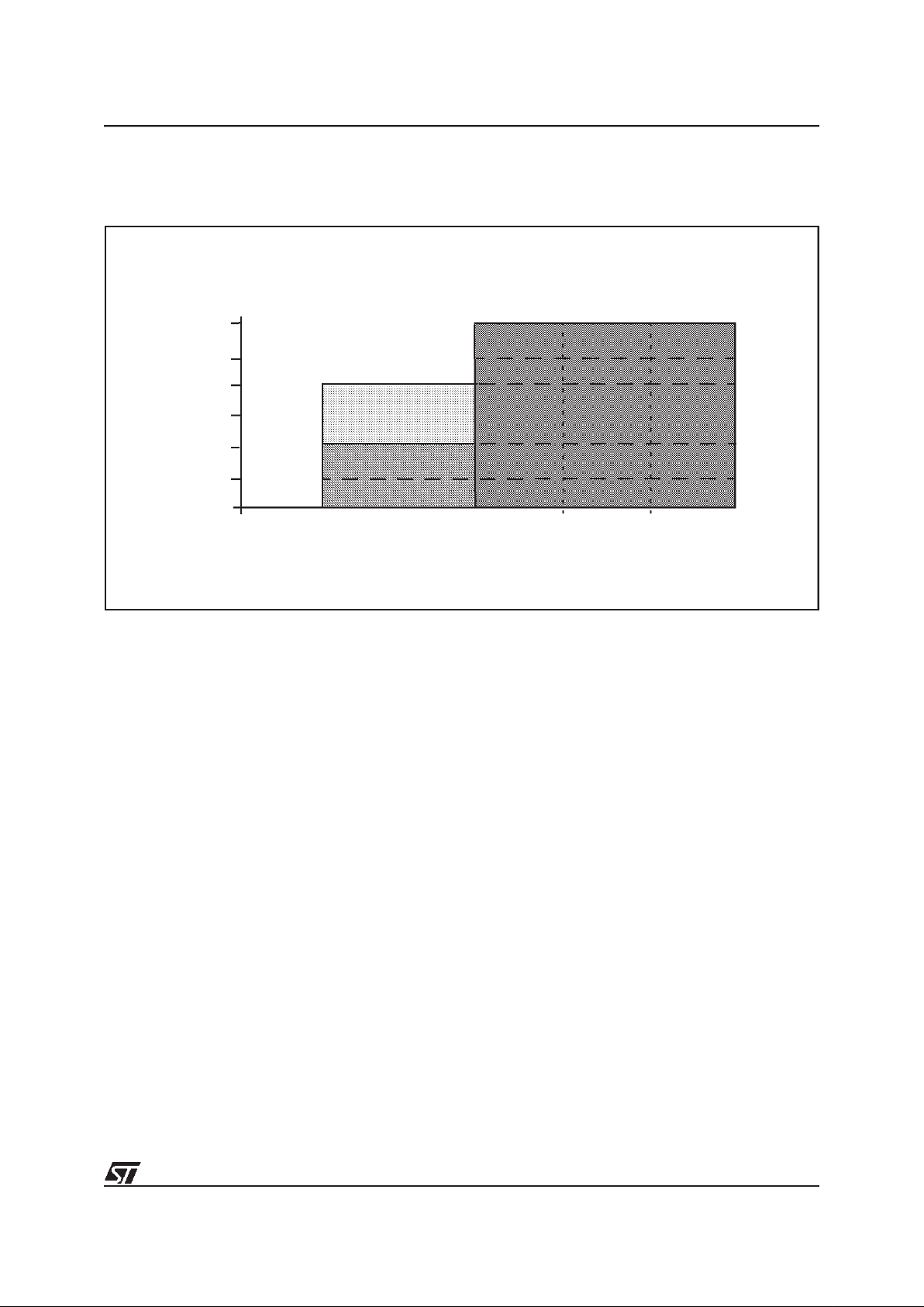
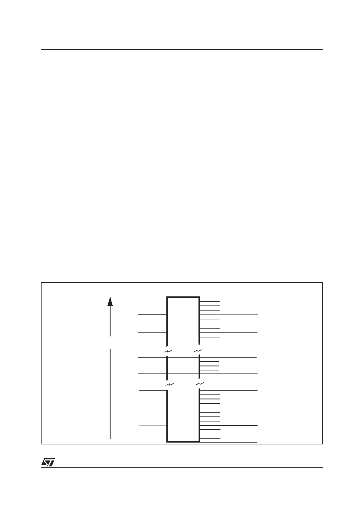
Figure 1, on page 7 shows the operating range of
the ST92163 devices.
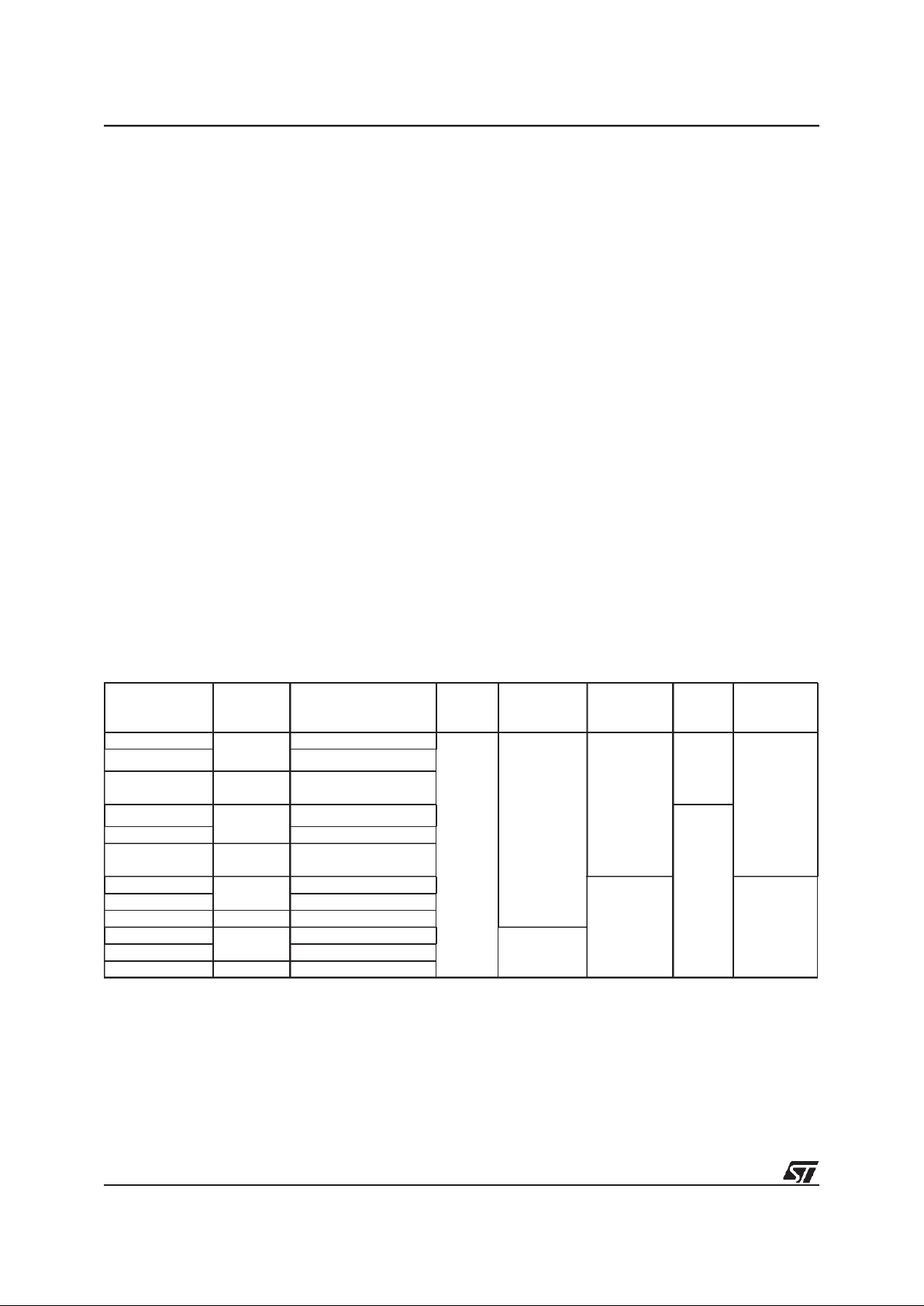
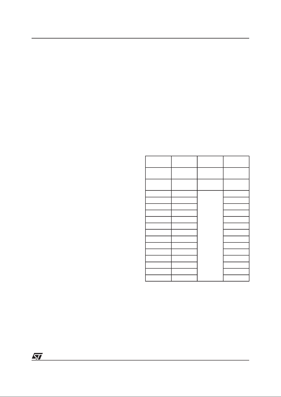
Device Summary
1
Contact sales office for availability
Device Package Program Memory RAM
16-MHz
Low Voltage
Mode
8-MHz
Low Voltage
Mode
LVD USB
ST92163
1
PSDIP56/
TQFP64
20K ROM
2K
No
No
Yes
Yes
ST92T163 20K OTP
ST92E163
CSDIP56/
CQFP64
20K EPROM
ST92163E
1
PSDIP56/
TQFP64
20K ROM
No
ST92T163E 20K OTP
ST92E163E
CSDIP56/
CQFP64
20K EPROM
ST92163L
1
TQFP64
20K ROM
Yes
In Normal
Mode only
ST92T163L 20K OTP
ST92E163L CQFP64 20K EPROM
ST92163V
1
TQFP64
20K ROM
YesST92T163V
1
20K OTP
ST92E163V
1
CQFP64 20K EPROM
Page 7
7/224
ST92163 - GENERAL DESCRIPTION
INTRODUCTION (Cont’d)
Figure 1. Maximum Operating Frequency (f
MAX
) versus Supply Voltage (VDD)
Notes:
1) This mode is supported by 16-MHz Low Voltage devices only
2) This mode is supported by 8-MHz Low Voltage devices and 16-MHz Low Voltage devices
3) This mode is supported by all devices
0
2.5
4 4.5 5 5.5
24
20
16
12
8
4
MAX FREQUENCY (MHz)
SUPPLY VOLTAGE (V)
3.0
16-MHz LOW VOLTAGE
MODE
1)
FUNCTIONALITY IS NOT
GUARANTEED
IN THIS AREA
NORMAL VOLTAGE MODE
3)
8-MHz LOW VOLTAGE
MODE
2)
Page 8
8/224
ST92163 - GENERAL DESCRIPTION
INTRODUCTION (Cont’d)
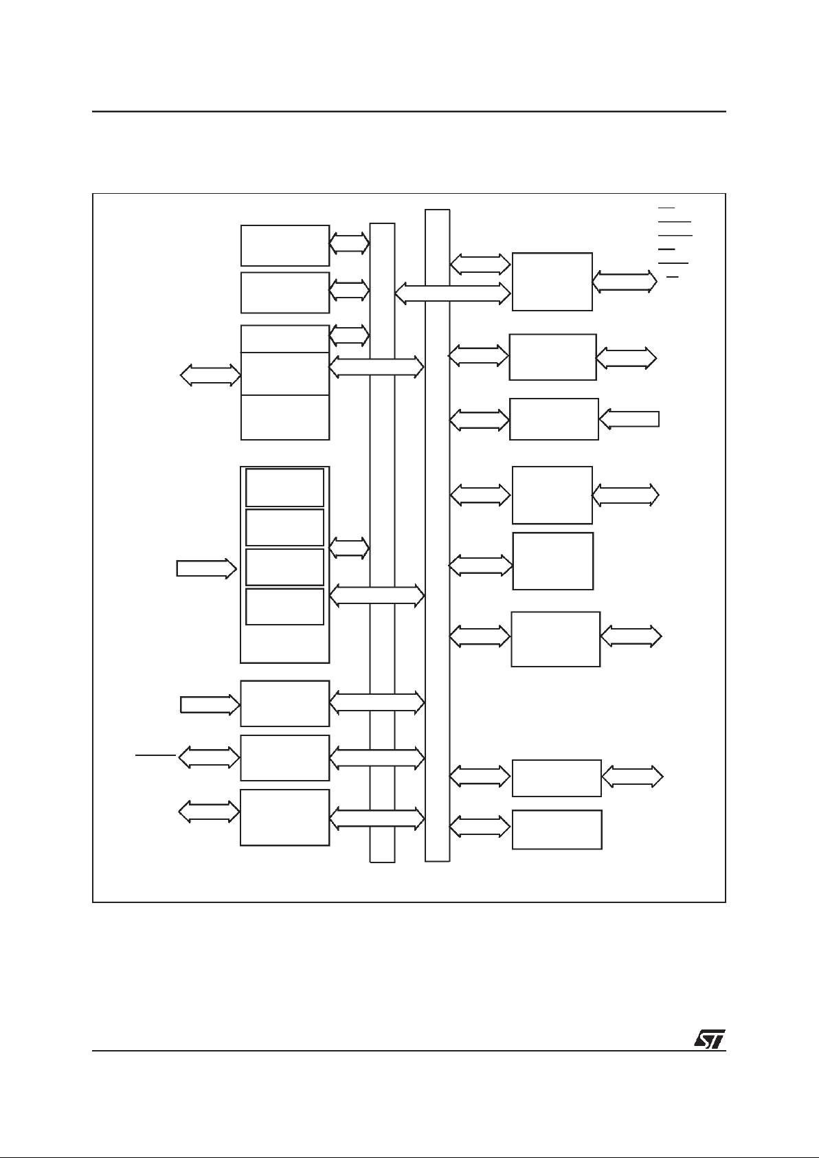
Figure 2. ST92163 Architectural Block Diagram
*64-pin devices only
**on some devices only (refer to “Device Summary” on page 6)
WATCHDOG
TIMER
256 bytes
Register File
2K RAM
ST9+ CORE
8/16-bit
CPU
Interrupt
Management
MEMORY BUS
RCCU
External
Memory
Interface
REGISTER BUS
A/D Converter
AS
BACK
BREQ
DS
WAIT
RW
P0[7:0]
SCI
20K ROM/
EPROM/OTP
AIN[5:0]
EXTRG
TXCLK
RXCLK
SIN
DCD
SOUT
CLKOUT
RTS
SDS
WDIN
WDOUT
All alternate functions (
Italic characters
) are mapped on Ports 0,1, 3, 4, 5 and 6
P3[7:0]
P1[7:0]
SDA
SCL
MF TIMER
USBGND
USBVCC
USBDM0
USBDP0
OSCIN
OSCOUT
RESET
INTCLK
I2C BUS
P5[7:0]
Fully Prog.
I/Os
TINA
TINB
TOUTA
TOUTB
INT[7:0]
NMI
P4[3:0]
P6[5:0]
USB
with 16 end-
points
Wakeup
and Interrupt
Management
WKUP[14:0]
P6[7:6]*
A[15:0]
D[7:0]
USBOE
DMA
DMA
9V/3.3V
Voltage
Regulator
Low Voltage
Detector
LVD**
USBSOF
MIRROR
REGISTER
Page 9

9/224
ST92163 - GENERAL DESCRIPTION
INTRODUCTION (Cont’d)
1.1.1 Core Architecture
The nucleus of the ST92163 is the enhanced ST9
Core that includes the Central Processing Unit
(CPU), theregister file, theinterrupt and DMA controller, and the Memory Management Unit (MMU).
Three independent buses are controlled by the
Core: a 22-bit memory bus, an 8-bit register addressing bus and a 6-bit interrupt/DMA bus which
connects the interrupt and DMA controllers in the
on-chip peripherals with the core.
This multiple bus architecture makes the ST9 family devices highly efficient foraccessing on and
off-chip memory and fast exchange of data with
the on-chip peripherals.
The general-purpose registers can be used as accumulators, index registers, or address pointers.
Adjacent registerpairs make up 16-bit registersfor
addressing or 16-bit processing. Although the ST9
has an 8-bit ALU, the chip handles 16-bit operations, including arithmetic, loads/stores, and memory/register and memory/memory exchanges.
Many opcodes specify byte or word operations,
the hardware automatically handles 16-bit operations and accesses.
For interrupts or subroutine calls, the CPU uses a
system stack in conjunction with the stack pointer
(SP). A separate user stack has its own SP. The
separate stacks, without size limitations, can be in
on-chip RAM (or in Register File) or off-chip memory.
1.1.2 Instruction Set
The ST9 instruction set consists of 94 instruction
types, including instructions for bit handling, byte
(8-bit) and word (16-bit) data, as well as BCD and
Boolean formats. Instructions have been added to
facilitate large program and data handling through
the MMU, as well as to improve the performance
and code density of C Function calls. 14 addressing modes are available, including powerful indirect addressing capabilities.
The bit-manipulation instructions of the ST9 are
set, clear,complement, testand set, load,and various logic instructions (AND, OR, and XOR). Math
functions include add, subtract, increment, decrement, decimal adjust, multiply and divide.
1.1.3 External MEMORY INTERFACE
The ST92163device has a16-bit external address
bus allowingit toaddress up to 64K bytes of external memory.
1.1.4 OPERATING MODES
To optimize performance versus the power consumption of the device, ST9 devices now support
a range of operating modes that can be dynamically selected depending on the performance and
functionality requirements of the application at a
given moment.
Run Mode. This is the full speed execution mode
with CPUand peripherals running at the maximum
clock speed delivered by the Phase Locked Loop
(PLL) of the Clock Control Unit (CCU).
Slow Mode. Power consumption can be significantly reduced byrunning theCPU and theperipherals at reduced clock speed using the CPU Prescaler and CCU Clock Divider.
Wait For Interrupt Mode. The Wait For Interrupt
(WFI) instruction suspends program executionuntil an interrupt request is acknowledged. During
WFI, the CPU clock is halted while the peripheral
and interrupt controller keep running at a frequency programmable via the CCU. In this mode, the
power consumption of the device can be reduced
by more than 95% (LP WFI).
Halt Mode. When executing the HALT instruction,
and if the Watchdog is not enabled, the CPU and
its peripherals stop operating and the status of the
machine remains frozen (the clock is also
stopped). A reset is necessary to exit from Halt
mode.
Stop Mode. Under user program control, (see
Wake-up and Interrupt Management Unit), the
CPU and its peripherals stop operating and the
status of the machine remains frozen (the clock is
also stopped) until program execution is woken up
by an event on an external Wake-up pin.
Page 10

10/224
ST92163 - GENERAL DESCRIPTION
INTRODUCTION (Cont’d)
1.1.5 On-chip Peripherals
USB Interface
The USB interface provides a full speed USB 1.1
compliant port with embedded transceiver and
voltage regulator. Upto 16 endpoints are available
supporting upto 8 USB devices.Separate transmit
and receive DMA channels are available for each
device for fast data transfers with internal RAM.
Parallel I/O Ports
The ST9 is providedwith dedicated lines for input/
output. These lines, grouped into 8-bit ports, can
be independently programmed to provide parallel
input/output or to carry input/output signals to or
from the on-chip peripherals and core. All ports
have active pull-ups and pull-down resistors compatible with TTL loads. In addition pull-ups can be
turned off for open drain operation and weak pullups can be turned on to save chip resistive pullups. Input buffers can be either TTL or CMOS
compatible.
High Current (10 mA) outputs are available for
driving external devices such as LEDs.
Multifunction Timer
The Multifunction Timer has a 16-bit Up/Down
counter supported by two 16-bit compare registers, two 16-bit input capture registers and two
DMA channels. Timing resolution can be programmed using an 8-bit prescaler. 12 operating
modes allow a range of different timing functions
to be easily performed suchas complex waveform
generatation, measurement or PWM output.
16-bit Timer/Watchdog
The Timer/Watchdog peripheral can be used as a
watchdog or for a wide range of other timing functions such asgenerating periodic interrupts,measuring input signal pulse widths, requesting an interrupt after a set number of events. It can also
generate a square wave or PWM output signal.
Serial Communications Controller
The SCIprovides a synchronous or asynchronous
serial I/O port using two DMA channels. Baud
rates and data formats are programmable. Controller applications can further benefit from the self
test and address wake-up facility offered by the
character search mode.
I2C Bus Interface
The I2C bus is a synchronous serial bus for connecting multiple devices using a data line and a
clock line. Multimaster and slave modes are supported. Data transfer between the bus and memory is performed by DMA. The I2C interface supports 7 and 10-bit addressing. It operates in multimaster or slave mode and supports speeds of up
to 400 KHz. Bus events (Bus busy, slave address
recognized) and error conditions are automatically
flagged in peripheral registers and interrupts are
optionally generated.
Analog/Digital Converter
The ADC provides up to 6 analog inputs with onchip sample and hold, fast conversion time and 8bit resolution. Conversion can be triggered by a
signal from the Multifunction Timer (MFT).
Page 11
11/224
ST92163 - GENERAL DESCRIPTION
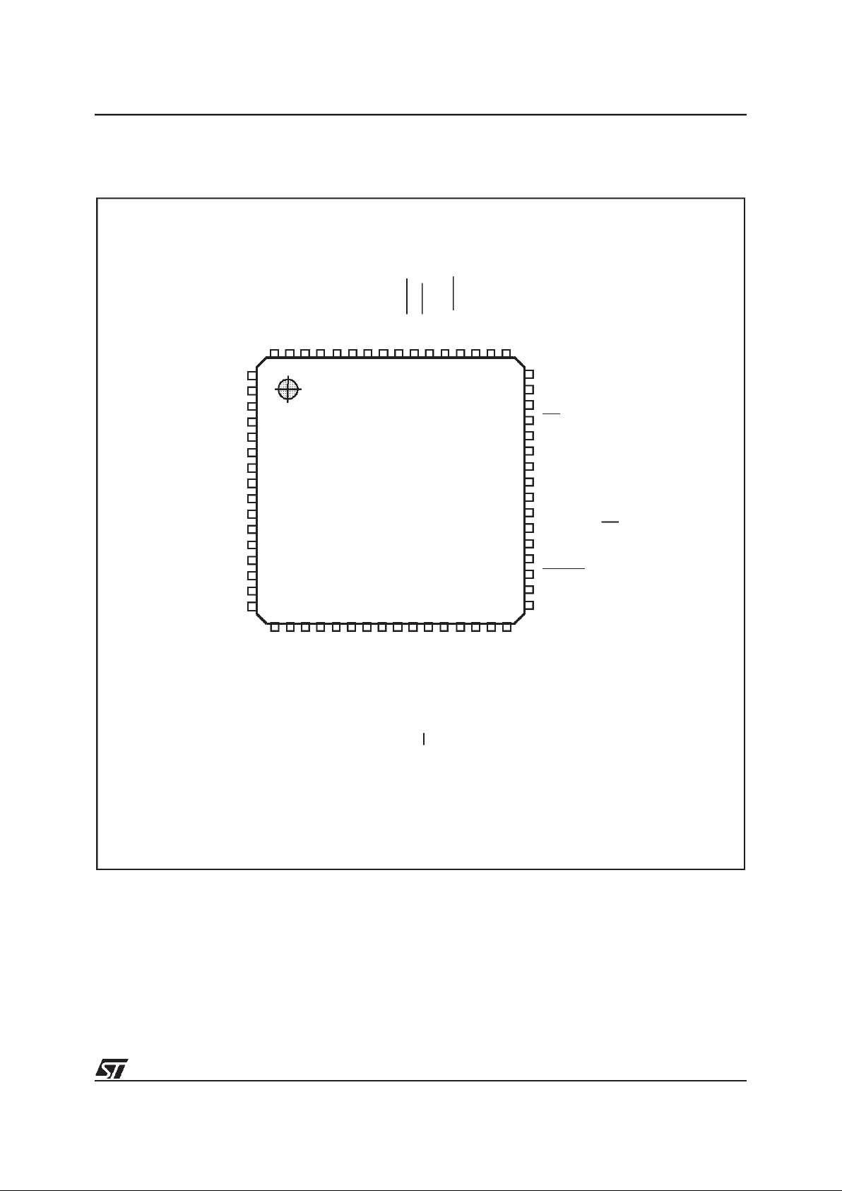
1.2 PIN DESCRIPTION
Figure 3. 64-Pin Package Pin-Out
N.C. = Not connected
WKUP14/A10/P1.2
WKUP14/A9/P1.1
WKUP14/A8/P1.0
D7/A7/P0.7
D6/A6/P0.6
D5/A5/P0.5
D4/A4/P0.4
D3/A3/P0.3
D2/A2/P0.2
D1/A1/P0.1
D0/A0/P0.0
AIN5/P6.7
AIN4/P6.6
USBSOF/AIN3/P6.5
USBSOF/AIN2/P6.4
WKUP13/AIN1/P6.3
P1.3/A11/WKUP14
P1.4/A12/WKUP14
P1.5/A13/WKUP14
P1.6/A14/WKUP14
P1.7/A15/WKUP14
N.C.
N.C.
VSSVDDP4.0/BREQ
P4.1/WAIT
P4.2
P4.3//BACK
USBDM0
USBDP0
N.C.
N.C.
USBVCC
USBGND
DS
P3.0/INT7/SOUT
P3.1/INT7/RTS
P3.2/INT7/TXCLK/CLKOUT
P3.3/INT7/RXCLK
P3.4/INT7/DCD
P3.5/INT7/SIN
P3.6/INT7/AS
P3.7/INT7/SDS
V
PP
RESET
P5.0/INT1/TINA
N.C.
AV
DD
WKUP12/AIN0/INTCLK/P6.2
WKUP11/SCL/EXTRG/INT6/P6.1
WKUP10/SDA/INT5/P6.0
V
DD
OSCIN
V
SS
OSCOUT
WDOUT/NMI/P5.7
WKUP9/TOUTB/P5.6
RW/WDIN/INT0/P5.5
USBOE/WKUP8/P5.4
TOUTA/INT2/P5.3
INT3/P5.2
TINB/INT4/P5.1
N.C.
1
64
16
32
48
16
Page 12
12/224
ST92163 - GENERAL DESCRIPTION
Figure 4. 56-Pin Package Pin-Out
Table 1. Power Supply Pins Table 2. Primary Function pins
156
2928
P3.4/INT7/DCD/WKUP4
P3.5/INT7/SIN/WKUP5
P3.6/INT7/ASN/WKUP6
P3.7/INT7/SDS/WKUP7
V
PP
RESET
P5.0/INT1/TINA
P5.1/INT4/TINB
P5.2/INT3
P5.3/INT2/TOUTA
P5.4/WKUP8/USBOE
P5.5/INT0/WDIN/RW
P5.6/TOUTB/WKUP9
P5.7/NMI/WDOUT
OSCOUT
V
SS
OSCIN
V
DD
P6.0/INT5/SDA/WKUP10
P6.1/INT6/EXTRG/SCL/WKUP11
P6.2/INTCLK/AIN0/WKUP12
AV
DD
P6.3/AIN1/WKUP13
P6.4/AIN2/USBSOF
P6.5/AIN3/USBSOF
P0.0/A0/D0
P0.1/A1/D1
P0.2/A2/D2
WKUP3/RXCLK/INT7/P3.3
WKUP2/CLKOUT/TXCLK/INT7/P3.2
WKUP1/RTS/INT7/P3.1
WKUP0/SOUT/INT7/P3.0
DS
USBGND
USBVCC
USBDP0
USBDM0
BACK/P4.3
P4.2
WAIT/P4.1
BREQ/P4.0
V
DD
V
SS
WKUP14/A15/P1.7
WKUP14/A14/P1.6
WKUP14/A13/P1.5
WKUP14/A12/P1.4
WKUP14/A11/P1.3
WKUP14/A10/P1.2
WKUP14/A9/P1.1
WKUP14/A8/P1.0
D7/A7/P0.7
D6/A6/P0.6
D5/A5/P0.5
D4/A4/P0.4
D3/A3/P0.3
Name Function
DIP56
QFP64
V
DD
Main Power Supply Voltage
(2 pins internally connected)
14 21
39 56
V
SS
Digital Circuit Ground
(2 pins internally connected)
15 23
41 57
AV
DD
Analog Circuit Supply Voltage 35 17
V
PP
EPROM Programming Voltage.
Must be connected to ground in
normal operating mode.
52 36
Name Function
DIP56
QFP64
DS Data Strobe 5 45
OSCIN Oscillator Input 40 22
OSCOUT Oscillator Output 42 24
RESET Reset to initialize the ST9 51 35
USBGND USB bus ground level 6 46
USBVCC USB voltage regulator output 7 47
USBDM0 USB Upstream port Data- line 9 51
USBDP0 USB Upstream port Data+ line 8 50
Page 13
13/224
ST92163 - GENERAL DESCRIPTION
1.3 I/O Port Pins
All the ports of the device can be programmed as
Input/Output or in Input mode, compatible with
TTL or CMOS levels (except where Schmitt Trigger is present). Each bit can be programmed individually (Refer to the I/O ports chapter).
TTL/CMOS Input
For all those port bits where no input schmitt trigger is implemented, it is always possible to program the input level as TTL or CMOS compatible
by programming the relevant PxC2.n control bit.
Refer I/O Ports Chapter to the section titled “Input/
Output Bit Configuration”.
Push-Pull/OD Output
The output buffer can be programmed as pushpull or open-drain: attention must be paid to the
fact thatthe open-drain option correspondsonly to
a disabling of P-channel MOS transistor of the
buffer itself: it is still present and physically connected to thepin. Consequentlyit isnot possible to
increase the output voltage on the pin over
VDD+0.3 Volt, to avoid direct junction biasing.
Pure Open-drain Output
The user can increase the voltage on an I/O pin
over VDD+0.3 Volt where theP-channel MOStransistor is physically absent: this is allowed on all
“Pure Open Drain” pins. Of course, in this case the
push-pull option is not available and any weak
pull-up must implemented externally.
Table 3. I/O Port Characteristics
Legend: WPU = Weak Pull-Up, OD = Open Drain
Input Output Weak Pull-Up Reset State
Port 0[7:0] TTL/CMOS Push-Pull/OD Yes Bidirectional WPU
Port 1[7:0] TTL/CMOS Push-Pull/OD Yes Bidirectional WPU
Port 3[7:0] Schmitt trigger Push-Pull/OD Yes Bidirectional WPU
Port 4[3:0] Schmitt trigger Push-Pull/OD Yes Bidirectional WPU
Port 5[7:0] Schmitt trigger Push-Pull/OD Yes Bidirectional WPU
Port 6[1:0]
Port 6[5:2]
Port 6.6
Port 6.7
Schmitt trigger
TTL/CMOS
Schmitt trigger
TTL/CMOS
Pure Open Drain with high sink capability
Push-Pull/OD with high sink capability
Push-Pull/OD with high sink capability
Push-Pull/OD with high sink capability
No
Yes
No
No
Bidirectional
Bidirectional WPU
Bidirectional
Bidirectional
Page 14

14/224
ST92163 - GENERAL DESCRIPTION
Table 4. ST92163 Alternate Functions
Port
Name
General
Purpose I/O
Pin
No.
Alternate Functions
DIP56
QFP64
P0.0
All ports useable
for general purpose I/O (input,
output or bidirectional)
31 11 A0/D0 I/O Ext. Mem. Address/Data bit 0
P0.1 30 10 A1/D1 I/O Ext. Mem. Address/Data bit 1
P0.2 29 9 A2/D2 I/O Ext. Mem. Address/Data bit 2
P0.3 28 8 A3/D3 I/O Ext. Mem. Address/Data bit 3
P0.4 27 7 A4/D4 I/O Ext. Mem. Address/Data bit 4
P0.5 26 6 A5/D5 I/O Ext. Mem. Address/Data bit 5
P0.6 25 5 A6/D6 I/O Ext. Mem. Address/Data bit 6
P0.7 24 4 A7/D7 I/O Ext. Mem. Address/Data bit 7
P1.0 23 3
A8 I/O Ext. Mem. Address bit 8
WKUP14 I Wakeup Line 14 (***)
P1.1 22 2
A9 I/O Ext. Mem. Address bit 9
WKUP14 I Wakeup Line 14 (***)
P1.2 21 1
A10 I/O Ext. Mem. Address bit 10
WKUP14 I Wakeup Line 14 (***)
P1.3 20 64
A11 I/O Ext. Mem. Address bit 11
WKUP14 I Wakeup Line 14 (***)
P1.4 19 63
A12 I/O Ext. Mem. Address bit 12
WKUP14 I Wakeup Line 14 (***)
P1.5 18 62
A13 I/O Ext. Mem. Address bit 13
WKUP14 I Wakeup Line 14 (***)
P1.6 17 61
A14 I/O Ext. Mem. Address bit 14
WKUP14 I Wakeup Line 14 (***)
P1.7 16 60
A15 I/O Ext. Mem. Address bit 15
WKUP14 I Wakeup Line 14 (***)
P3.0 4 44
WKUP0 I Wakeup Line 0
INT7 I External Interrupt 7 (*)
SOUT O SCI Data Output
P3.1 3 43
WKUP1 O Wakeup Line 1
INT7 I External Interrupt 7 (*)
RTS O SCI Request to Send
Page 15

15/224
ST92163 - GENERAL DESCRIPTION
P3.2
All ports useable
for general purpose I/O (input,
output or bidirec-
tional)
242
WKUP2 I Wakeup Line 2
INT7 I External Interrupt 7 (*)
TXCLK I SCI Transmit CK Input
CLKOUT O SCI Clock Output
P3.3 1 41
WKUP3 I Wakeup Line 3
INT7 I External Interrupt 7 (*)
RXCLK I SCI Receive CK Input
O
P3.4 56 40
WKUP4 I Wakeup Line 4
INT7 I External Interrupt 7 (*)
DCD I SCI Data Carrier Detect
O
P3.5 55 39
WKUP5 I Wakeup Line 5
INT7 I External Interrupt 7 (*)
SIN I SCI Data Input
O
P3.6 54 38
WKUP6 I Wakeup Line 6
INT7 I External Interrupt 7 (*)
AS (**) O Ext. Mem. Address Strobe
P3.7 53 37
WKUP7 I Wakeup Line 7
INT7 I External Interrupt 7 (*)
SDS O SCI Synchronous Data Send
P4.0 13 55 BREQ I Ext. Mem. Bus Request
P4.1 12 54
WAIT I Ext. Mem. Wait Input
RW O Ext. Mem. Read/Write Mode Select
P4.2 11 53
I
AS (**) O Ext. Mem. Address Strobe
P4.3 10 52
I
BACK O Ext. Mem. bus acknow
Port
Name
General
Purpose I/O
Pin
No.
Alternate Functions
DIP56
QFP64
Page 16
16/224
ST92163 - GENERAL DESCRIPTION
P5.0
All ports useable
for general purpose I/O (input,
output or bidirectional)
50 34
INT1 I External Interrupt 1
TINA I MF Timer Input A
O
P5.1 49 31
INT4 I External Interrupt 4
TINB I MF Timer Input B
O
P5.2 48 30 INT3 I External Interrupt 3
P5.3 47 29
INT2 I External Interrupt 2
TOUTA O MF Timer Output A
P5.4 46 28
WKUP8 I Wakeup Line 8
USBOE O USB Outputenable
P5.5 45 27
WDIN I Watchdog TimerInput
INT0 I External Interrupt 0
RW O Ext. Mem. Read/Write Mode Select
P5.6 44 26
WKUP9 I Wakeup Line 9
TOUTB O MF Timer Output B
P5.7 43 25
NMI I Non Maskable Interrupt
WDOUT O Watchdog Timer Output
P6.0 38 20
WKUP10 I Wakeup Line 10
INT5 I External Interrupt 5
SDAI I I
2
C Bus Data In
SDAO O I
2
C Bus Data Out
P6.1 37 19
WKUP11 I Wakeup Line 11
INT6 I External Interrupt 6
SCLI I I
2
C Bus Clock In
EXTRG I A/D External Trigger
SCLO O I
2
C Bus Clock Out
P6.2 36 18
AIN0 I A/D Analog Input 0
WKUP12 I Wakeup Line 12
INTCLK O Internal Clock
P6.3 34 16
WKUP13 I Wakeup Line 13
AIN1 I A/D Analog Input 1
O
Port
Name
General
Purpose I/O
Pin
No.
Alternate Functions
DIP56
QFP64
Page 17
17/224
ST92163 - GENERAL DESCRIPTION
*Eight interrupt lines internally connected to INT7
through a boolean AND function.
** AS cannot be disabled by software if the ASAF
bit is set (Page Register 245) once the corresponding P3.6 bit is configured as an Alternate
Function output.
***Eight wakeup lines internally connected to
WKUP14 through a boolean AND function.
Note: The reset state of Port 0 and Port 1 is Input,
Weak Pull-Up. To interface external memory, the
ports must be configured by software as alternate
function output.
P6.4
All ports useable
for general purpose I/O (input,
output or bidirectional)
33 15
AIN2 I A/D Analog Input 2
USBSOF O USB SOFSynchro
P6.5 32 14 AIN3 I A/D Analog Input 3
USBSOF O USB SOFSynchro
P6.6 - 13
AIN4 I A/D Analog Input 4
O
P6.7 - 12
AIN5 I A/D Analog Input 5
O
Port
Name
General
Purpose I/O
Pin
No.
Alternate Functions
DIP56
QFP64
Page 18

18/224
ST92163 - GENERAL DESCRIPTION
How to configure the I/O ports
To configure the I/O ports, use the information in
Table 3 and Table 4 and the Port Bit Configuration
Table in the I/O Ports Chapter on page 100.
I/O Note = the hardware characteristics fixed for
each port line.
Inputs:
– If I/O note= TTL/CMOS, either TTL or CMOS in-
put level can be selected by software.
– If I/O note = Schmitt trigger, selecting CMOS or
TTL inputby software hasno effect, the inputwill
always be Schmitt Trigger.
Outputs:
– If I/O note= Push-Pull, either Push Pull or Open
Drain can be selectedby software.
– If I/O note = Open Drain, selecting Push-Pull by
software has no effect, the input will always be
Open Drain.
Alternate Functions (AF) = More than one AF
cannot be assigned to an external pin at the same
time: it can be selected as follows, but simultaneous availability of several functions of one pin is
obviously impossible.
AF Inputs:
– AF is selected implicitly by enablingthe corre-
sponding peripheral. Exceptions tothis areADC
inputs which are selected explicitly as AF bysoft-
ware.
AF Outputs or Bidirectional Lines:
– In the case of Outputs or I/Os, AF is selected
explicitly by software.
Example 1: Timer/Watchdog input
AF: WDIN, Port: P5.5, I/O note: InputSchmitt Trigger.
Write the port configuration bits:
P5C2.5=1
P5C1.5=0
P5C0.5=1
Enable the WDT peripheral by software as de-
scribed in the WDT chapter.
Example 2: Timer/Watchdog output
AF: WDOUT, Port: P5.7, I/O note: None
Write the port configuration bits:
P5C2.7=0
P5C1.7=1
P5C0.7=1
Example 3: ADC input
AF: AIN0, Port: P6.2, I/O note: Does not apply to
ADC
Write the port configuration bits:
P6C2.2=1
P6C1.2=1
P6C0.2=1
Page 19
19/224
ST92163 - GENERAL DESCRIPTION
1.4 MEMORY MAP
Figure 5. ST92163 Memory Map
SEGMENT 20h
64 Kbytes
200000h
21FFFFh
20C000h
20BFFFh
208000h
207FFFh
204000h
203FFFh
PAGE 80 - 16 Kbytes
PAGE 81 - 16 Kbytes
PAGE 82 - 16 Kbytes
PAGE 83 - 16 Kbytes
20F800h
20FFFFh
Note: Internal RAM addresses are
RAM
2 Kbytes
Reserved
Internal
External
Memory
Reserved
External
Memory
SEGMENT 21h
64 Kbytes
Internal ROM/EPROM
20FFFFh
220000h
3FFFFFh
repeated each 2 Kbytes inside segment 20h.
Lower Memory
(usually external ROM/EPROM
Upper Memory
(usually external RAM mapped
210000h
Note: The total amount of external memory is 64 Kbytes.
mapped in Segment 1)
in Segment 23h)
1FFFFFh
010000h
00FFFFh
00C000h
00BFFFh
008000h
007FFFh
004000h
000000h
003FFFh
PAGE 0 - 16 Kbytes
PAGE 1 - 16 Kbytes
PAGE 2 - 16 Kbytes
PAGE 3 - 16 Kbytes
64 Kbytes
SEGMENT 0
000000h
004FFFh
ROM/EPROM
20 Kbytes
Internal
Page 20

20/224
ST92163 - GENERAL DESCRIPTION
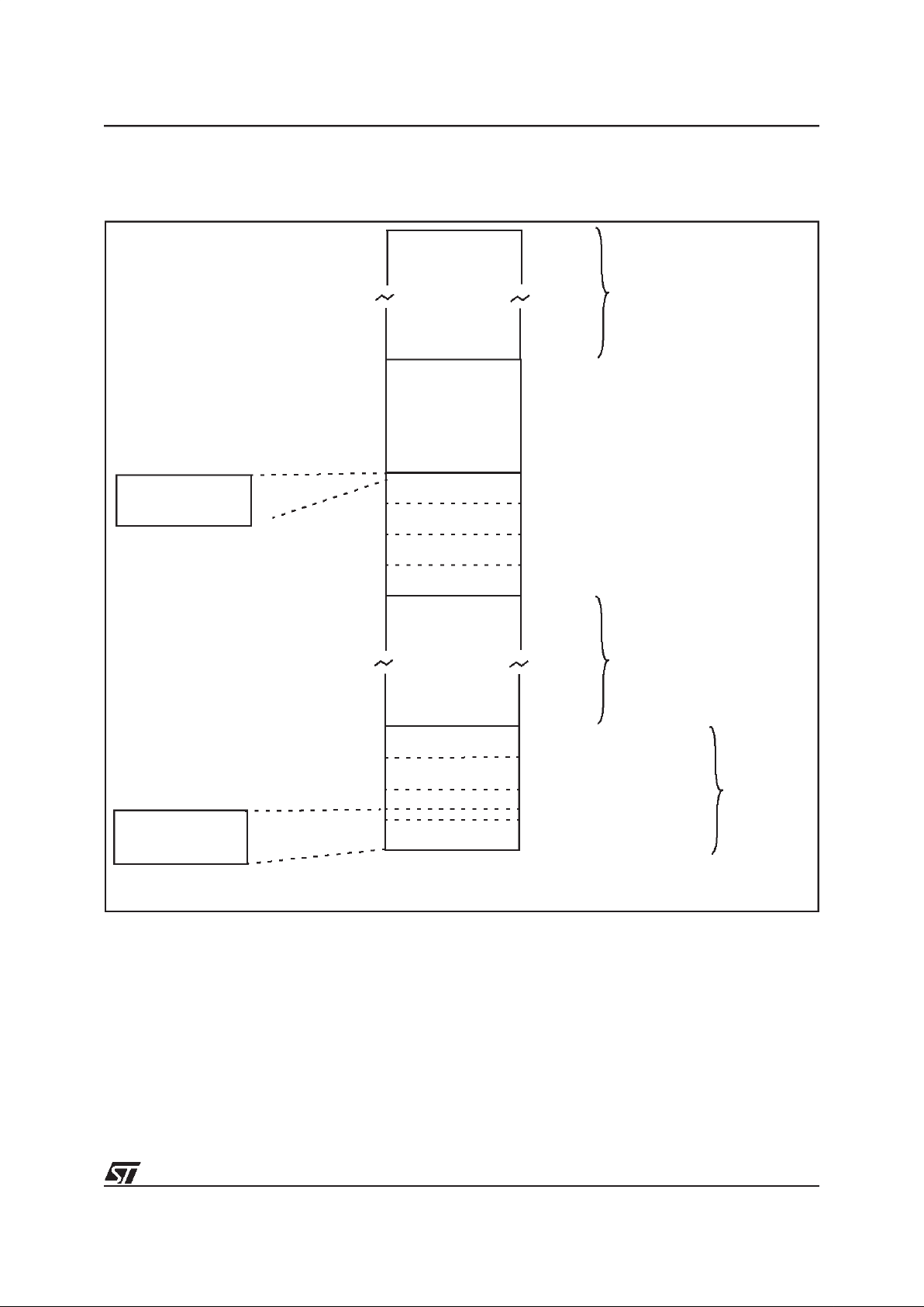
1.5 ST92163 REGISTER MAP
Table 6 contains themap of thegroup Fperipheral
pages.
The common registers used by each peripheral
are listed in Table 5.
Be very careful to correctly program both:
– The set of registersdedicated to a particular
function or peripheral.
– Registers common to other functions.
– In particular, double-check that any registers
with “undefined” resetvalues have been correct-
ly initialized.
Warning: Notethat in the EIVR and each IVR reg-
ister, all bits are significant. Take care when defining base vector addresses that entriesin theInterrupt Vector table do not overlap.
Table 5. Common Registers
Figure 6. ST92163 Register Groups
Function or Peripheral Common Registers
SCI, MFT CICR + NICR + DMA REGISTERS+ I/O PORT REGISTERS
ADC CICR + NICR + I/O PORT REGISTERS
WDT
CICR + NICR + EXTERNAL INTERRUPT REGISTERS +
I/O PORT REGISTERS
I/O PORTS I/O PORT REGISTERS + MODER
EXTERNAL INTERRUPT INTERRUPT REGISTERS + I/O PORT REGISTERS
RCCU INTERRUPT REGISTERS + MODER
REGISTER FILE
SYSTEM REGISTERS
255
240
239
224
223
F
E
D
C
B
A
9
8
7
6
5
4
3
2
1
0
15
00
PAGED REGISTERS
These register groups (16 registers per group)
The amount of reserved registers depends on
the number of endpoints used in the program.
(8 registers are used per endpoint).
for USB DMA.are potentially reserved
Page 21

21/224
ST92163 - GENERAL DESCRIPTION
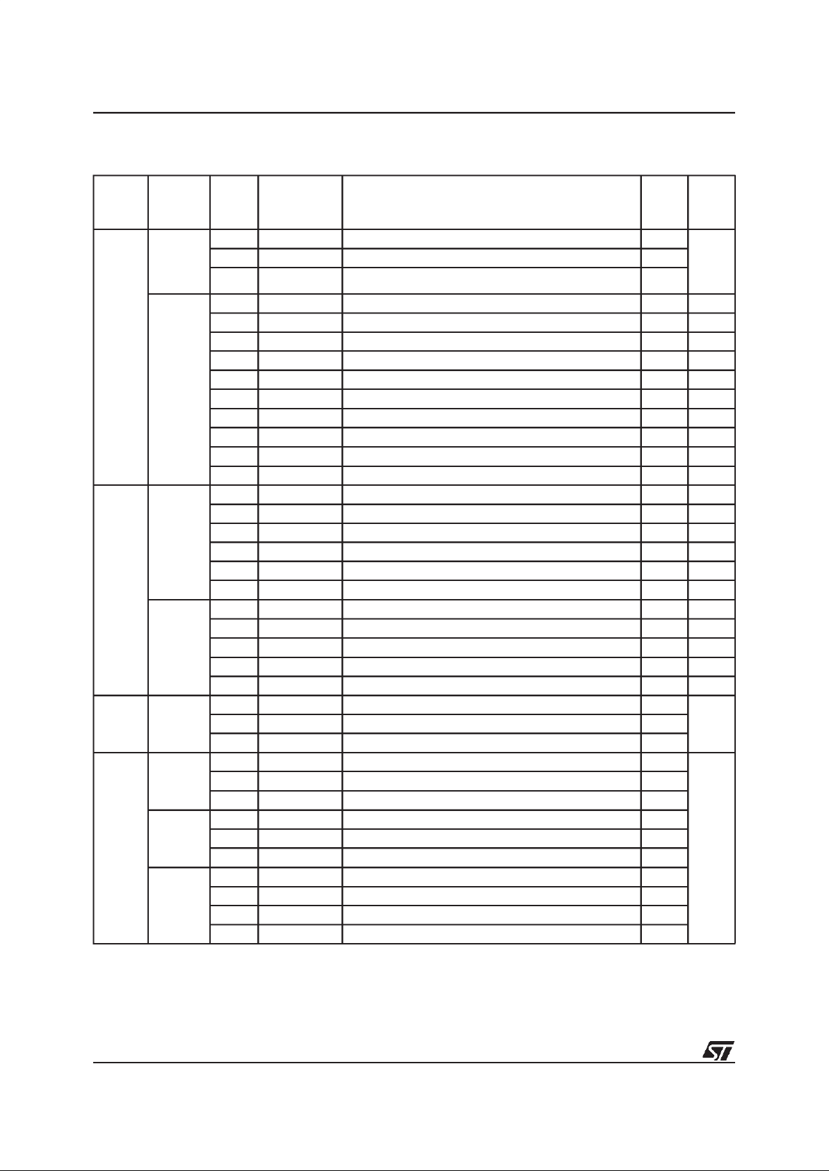
Table 6. Group F Pages Register Map
Resources available on the ST92163 device:
Register
Page
0 2 3 4 5 9 101520212443555762
R255
Res.
Res.
Res.
USB
Endpoints
Res.
MFT
USB
Com-
mon
I2C MMU SCI
Port
9
Res.
WUI
MU
ADC
R254
Port
3
R253
R252 WCR
R251
WDT
Res.
Port
6
Port
8
R250
R249
R248
Res.
R247
EXT
INT
Res.
Res.
R246
Port
5
RCCU
R245
R244
R243 Res.
MFT
R242
Port
4
R241
Res.
R240
Page 22
22/224
ST92163 - GENERAL DESCRIPTION
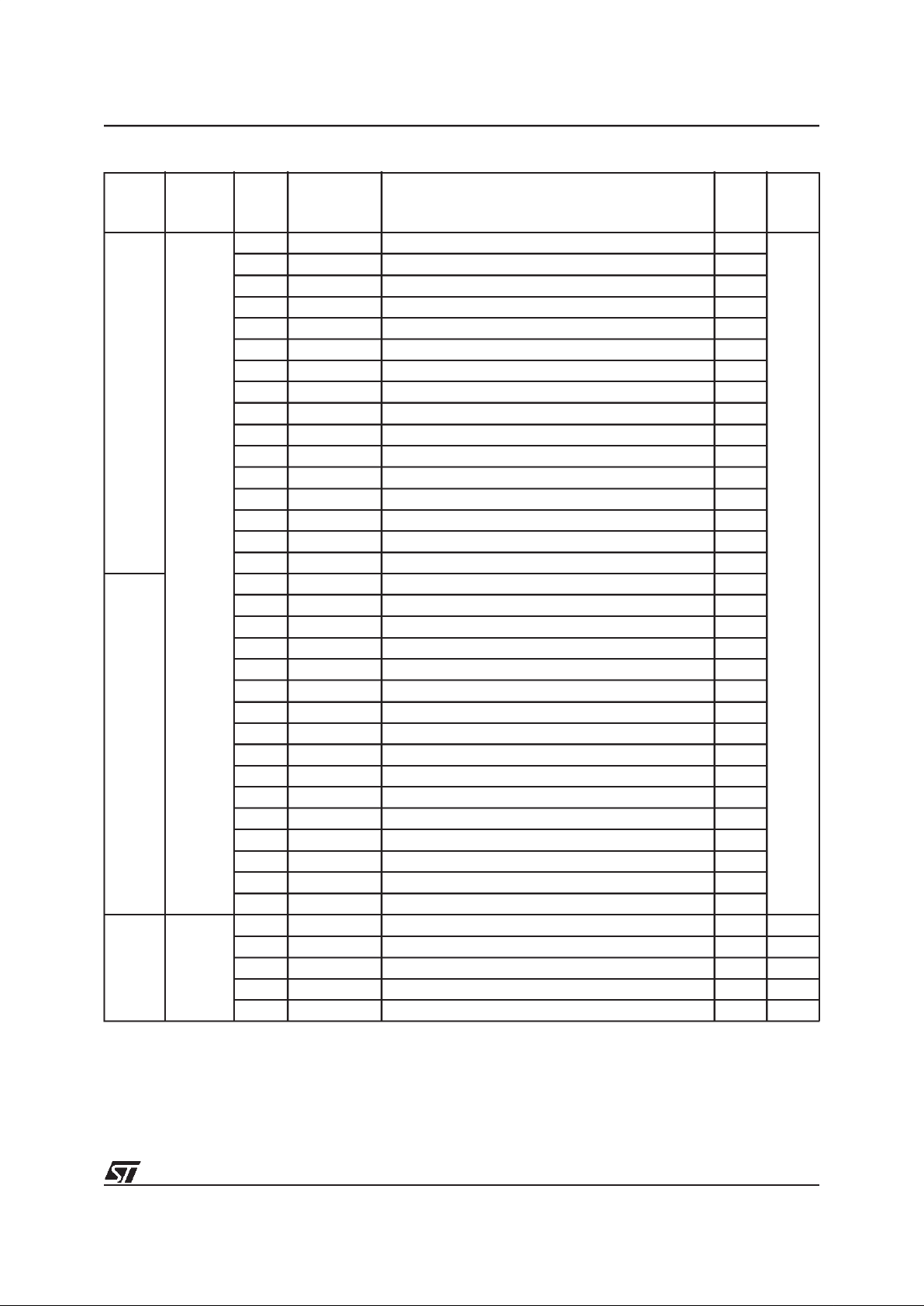
Table 7. Detailed Register Map
Page
No.
Block
Reg.
No.
Register
Name
Description
Reset
Value
Hex.
Doc.
Page
System
I/O
Port
3:5
R227 P3DR Port 3 Data Register FF
98
R228 P4DR Port 4 Data Register FF
R229 P5DR Port 5 Data Register FF
Core
R230 CICR Central Interrupt Control Register 87 30
R231 FLAGR Flag Register 00 31
R232 RP0 Pointer 0 Register 00 33
R233 RP1 Pointer 1 Register 00 33
R234 PPR Page Pointer Register 54 35
R235 MODER Mode Register E0 35
R236 USPHR User Stack Pointer High Register xx 37
R237 USPLR User Stack Pointer Low Register xx 37
R238 SSPHR System Stack Pointer High Reg. xx 37
R239 SSPLR System Stack Pointer Low Reg. xx 37
0
INT
R242 EITR External Interrupt Trigger Register 00 59
R243 EIPR External Interrupt Pending Reg. 00 60
R244 EIMR External Interrupt Mask-bit Reg. 00 60
R245 EIPLR External Interrupt Priority Level Reg. FF 60
R246 EIVR External Interrupt Vector Register x6 61
R247 NICR Nested Interrupt Control 00 61
WDT
R248 WDTHR Watchdog Timer High Register FF 109
R249 WDTLR Watchdog Timer Low Register FF 109
R250 WDTPR Watchdog Timer Prescaler Reg. FF 109
R251 WDTCR Watchdog Timer Control Register 12 109
R252 WCR Wait Control Register 7F 110
2
I/O
Port
3
R252 P3C0 Port 3 Configuration Register 0 00
98R253 P3C1 Port 3 Configuration Register 1 00
R254 P3C2 Port 3 Configuration Register 2 00
3
I/O
Port
4
R240 P4C0 Port 4 Configuration Register 0 00
98
R241 P4C1 Port 4 Configuration Register 1 00
R242 P4C2 Port 4 Configuration Register 2 00
I/O
Port
5
R244 P5C0 Port 5 Configuration Register 0 00
R245 P5C1 Port 5 Configuration Register 1 00
R246 P5C2 Port 5 Configuration Register 2 00
I/O
Port
6
R248 P6C0 Port 6 Configuration Register 0 00
R249 P6C1 Port 6 Configuration Register 1 00
R250 P6C2 Port 6 Configuration Register 2 00
R251 P6DR Port 6 Data Register FF
Page 23
23/224
ST92163 - GENERAL DESCRIPTION
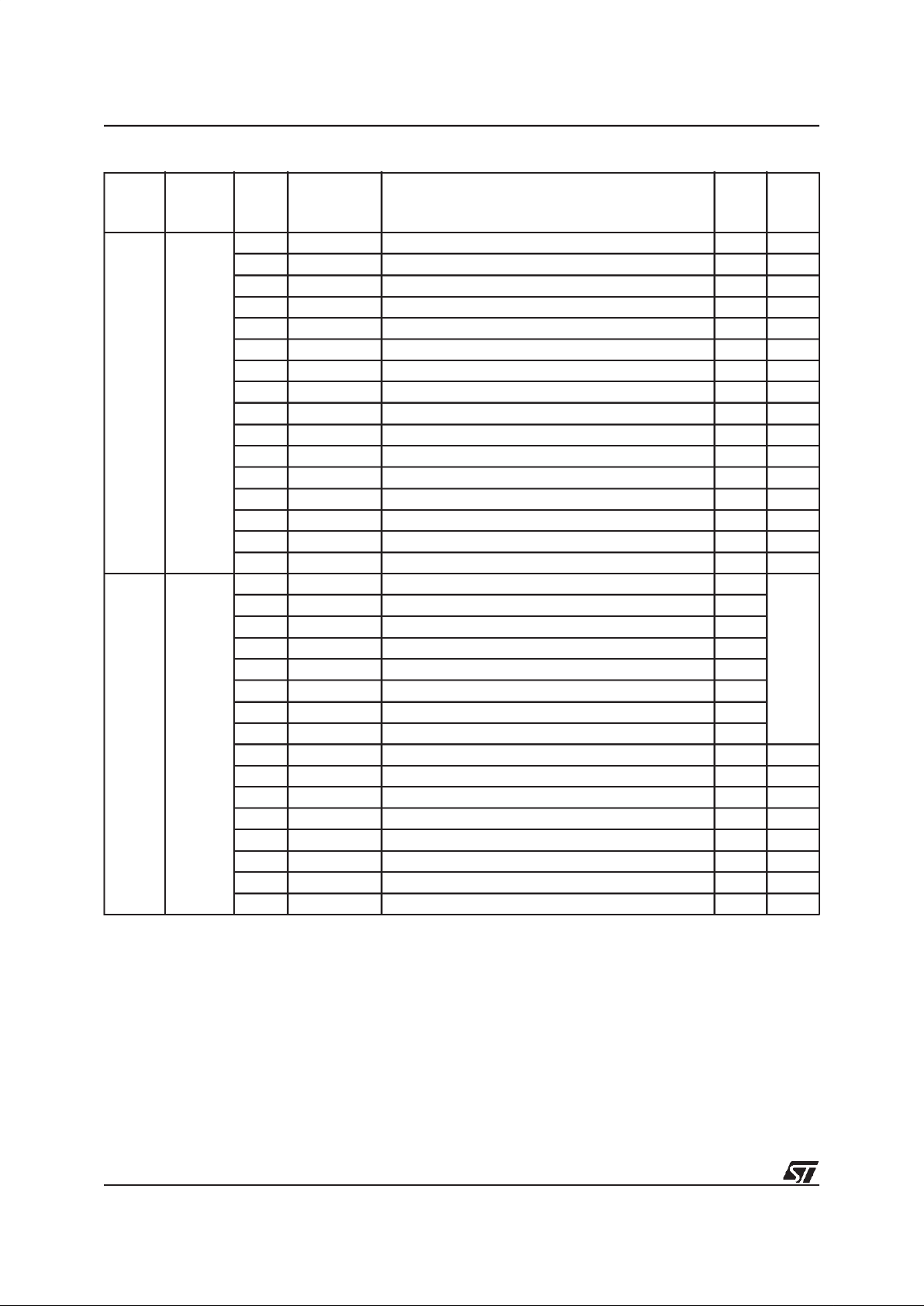
4
USB
End
Points
R240 EP0RA Endpoint 0 Register A (Transmission) 00
143
R241 EP0RB Endpoint 0 Register B (Reception) 00
R242 EP1RA Endpoint 1 Register A (Transmission) 00
R243 EP1RB Endpoint 1 Register B (Reception) 00
R244 EP2RA Endpoint 2 Register A (Transmission) 00
R245 EP2RB Endpoint 2 Register B (Reception) 00
R246 EP3RA Endpoint 3 Register A (Transmission) 00
R247 EP3RB Endpoint 3 Register B (Reception) 00
R248 EP4RA Endpoint 4 Register A (Transmission) 00
R249 EP4RB Endpoint 4 Register B (Reception) 00
R250 EP5RA Endpoint 5 Register A (Transmission) 00
R251 EP5RB Endpoint 5 Register B (Reception) 00
R252 EP6RA Endpoint 6 Register A (Transmission) 00
R253 EP6RB Endpoint 6 Register B (Reception) 00
R254 EP7RA Endpoint 7 Register A (Transmission) 00
R255 EP7RB Endpoint 7 Register B (Reception) 00
5
R240 EP8RA Endpoint 8 Register A (Transmission) 00
R241 EP8RB Endpoint 8 Register B (Reception) 00
R242 EP9RA Endpoint 9 Register A (Transmission) 00
R243 EP9RB Endpoint 9 Register B (Reception) 00
R244 EP10RA Endpoint 10 Register A (Transmission) 00
R245 EP10RB Endpoint 10 Register B (Reception) 00
R246 EP11RA Endpoint 11 Register A (Transmission) 00
R247 EP11RB Endpoint 11 Register B (Reception) 00
R248 EP12RA Endpoint 12 Register A (Transmission) 00
R249 EP12RB Endpoint 12 Register B (Reception) 00
R250 EP13RA Endpoint 13 Register A (Transmission) 00
R251 EP13RB Endpoint 13 Register B (Reception) 00
R252 EP14RA Endpoint 14 Register A (Transmission) 00
R253 EP14RB Endpoint 14 Register B (Reception) 00
R254 EP15RA Endpoint 15 Register A (Transmission) 00
R255 EP15RB Endpoint 15 Register B (Reception) 00
9 MFT
R240 DCPR DMA Counter Pointer Register xx 132
R241 DAPR DMA Address Pointer Register xx 133
R242 T_IVR Interrupt Vector Register xx 133
R243 IDCR Interrupt/DMA Control Register C7 134
R248 IOCR I/O Connection Register FC 134
Page
No.
Block
Reg.
No.
Register
Name
Description
Reset
Value
Hex.
Doc.
Page
Page 24
24/224
ST92163 - GENERAL DESCRIPTION
10 MFT
R240 REG0HR Capture Load Register 0 High xx 125
R241 REG0LR Capture Load Register 0 Low xx 125
R242 REG1HR Capture Load Register 1 High xx 125
R243 REG1LR Capture Load Register 1 Low xx 125
R244 CMP0HR Compare 0 Register High 00 125
R245 CMP0LR Compare 0 Register Low 00 125
R246 CMP1HR Compare 1 Register High 00 125
R247 CMP1LR Compare 1 Register Low 00 125
R248 TCR Timer Control Register 0x 126
R249 TMR Timer Mode Register 00 127
R250 T_ICR External Input Control Register 0x 128
R251 PRSR Prescaler Register 00 128
R252 OACR Output A Control Register xx 129
R253 OBCR Output B Control Register xx 130
R254 T_FLAGR Flags Register 00 31
R255 IDMR Interrupt/DMA MaskRegister 00 132
15
USB
Common
R240 DADDR0 Device Address Register 0 00
143
R241 DADDR1 Device Address Register 1 00
R242 DADDR2 Device Address Register 2 00
R243 DADDR3 Device Address Register 3 00
R244 DADDR4 Device Address Register 4 00
R245 DADDR5 Device Address Register 5 00
R246 DADDR6 Device Address Register 6 00
R247 DADDR7 Device Address Register 7 00
R248 USBIVR USB Interrupt Vector Register xx 139
R249 USBISTR USB Interrupt Status Register 00 139
R250 USBIMR USB Interrupt Mask Register 00 140
R251 USBIPR USB Interrupt Priority Register xx 140
R252 USBCTLR USB Control Register 17 141
R253 CTRINF CTR Interrrupt Flags xx 142
R254 FNRH Frame Number Register High 0x 142
R255 FNRL Frame Number Register Low xx 142
Page
No.
Block
Reg.
No.
Register
Name
Description
Reset
Value
Hex.
Doc.
Page
Page 25
25/224
ST92163 - GENERAL DESCRIPTION
20 I2C
R240 I2CCR I
2
C Control Register 00 186
R241 I2CSR1 I
2
C Status Register 1 00 187
R242 I2CSR2 I
2
C Status Register 2 00 189
R243 I2CCCR I
2
C Clock Control Register 00 190
R244 I2COAR1 I
2
C Own Address Register 1 00 190
R245 I2COAR2 I
2
C Own Address Register 2 00 191
R246 I2CDR I
2
C Data Register 00 191
R247 I2CADR I
2
C General Call Address A0 191
R248 I2CISR I
2
C Interrupt Status Register xx 192
R249 I2CIVR I
2
C Interrupt Vector Register xx 193
R250 I2CRDAP Receiver DMA Source Addr. Pointer xx 193
R251 I2CRDC Receiver DMA Transaction Counter xx 193
R252 I2CTDAP Transmitter DMA Source Addr. Pointer xx 194
R253 I2CTDC Transmitter DMA Transaction Counter xx 194
R254 I2CECCR I
2
C Extended Clock Control Register 00 194
R255 I2CIMR I
2
C Interrupt Mask Register x0 195
21
MMU
R240 DPR0 Data Page Register 0 00 42
R241 DPR1 Data Page Register 1 01 42
R242 DPR2 Data Page Register 2 02 42
R243 DPR3 Data Page Register 3 83 42
R244 CSR Code Segment Register 00 43
R248 ISR Interrupt Segment Register x0 43
R249 DMASR DMA Segment Register x0 43
EXTMI
R245 EMR1 External Memory Register 1 80 95
R246 EMR2 External Memory Register 2 0F 96
24 SCI
R240 RDCPR Receiver DMA Transaction Counter Pointer xx 165
R241 RDAPR Receiver DMA Source Address Pointer xx 165
R242 TDCPR Transmitter DMA Transaction Counter Pointer xx 165
R243 TDAPR Transmitter DMADestination Address Pointer xx 165
R244 S_IVR Interrupt Vector Register xx 166
R245 ACR Address/Data Compare Register xx 166
R246 IMR Interrupt Mask Register x0 167
R247 S_ISR Interrupt Status Register xx 43
R248 RXBR Receive Buffer Register xx 169
R248 TXBR Transmitter Buffer Register xx 169
R249 IDPR Interrupt/DMA Priority Register xx 170
R250 CHCR Character Configuration Register xx 171
R251 CCR Clock Configuration Register 00 172
R252 BRGHR Baud Rate Generator High Reg. xx 173
R253 BRGLR Baud Rate Generator Low Register xx 173
R254 SICR Synchronous Input Control 03 173
R255 SOCR Synchronous Output Control 01 174
Page
No.
Block
Reg.
No.
Register
Name
Description
Reset
Value
Hex.
Doc.
Page
Page 26
26/224
ST92163 - GENERAL DESCRIPTION
Note: xx denotes a byte with an undefined value, but some bits may have defined values. See register description for de-
tails.
43
I/O
Port
8
R248 P8C0 Port 8 Configuration Register 0 00
98
R249 P8C1 Port 8 Configuration Register 1 00
R250 P8C2 Port 8 Configuration Register 2 00
R251 P8DR Port 8 Data Register FF
I/O
Port
9
R252 P9C0 Port 9 Configuration Register 0 00
R253 P9C1 Port 9 Configuration Register 1 00
R254 P9C2 Port 9 Configuration Register 2 00
R255 P9DR Port 9 Data Register FF
55 RCCU
R240 CLKCTL Clock Control Register 00 81
R242 CLK_FLAG Clock Flag Register
48, 28
or 08
82
R246 PLLCONF PLL Configuration Register xx 83
59 WUIMU
R249 WUCTRL Wake-Up Control Register 00 67
R250 WUMRH Wake-Up Mask Register High 00 68
R251 WUMRL Wake-Up Mask Register Low 00 68
R252 WUTRH Wake-Up Trigger Register High 00 69
R253 WUTRL Wake-Up Trigger Register Low 00 69
R254 WUPRH Wake-Up Pending Register High 00 69
R255 WUPRL Wake-Up Pending Register Low 00 69
60 USB
R244 DEVCONF1 USB device configuration 1 0F 146
R245 DEVCONF2 USB device configuration 2 00 146
R246 MIRRA Mirror Register A xx 147
R247 MIRRB Mirror Register B xx 147
62 ADC
R240 ADDTR Channel i Data Register xx 199
R241 ADCLR Control Logic Register 00 199
R242 ADINT AD Interrupt Register 01 200
Page
No.
Block
Reg.
No.
Register
Name
Description
Reset
Value
Hex.
Doc.
Page
Page 27
27/224
ST92163 - DEVICE ARCHITECTURE
2 DEVICE ARCHITECTURE
2.1 CORE ARCHITECTURE
The ST9+ Core or Central Processing Unit (CPU)
features ahighly optimised instructionset, capable
of handling bit, byte (8-bit) and word (16-bit) data,
as well as BCDand Boolean formats; 14 addressing modes are available.
Four independent buses are controlled by the
Core: a 16-bit Memory bus, an 8-bit Register data
bus, an 8-bit Register address bus and a 6-bit Interrupt/DMA bus which connects the interrupt and
DMA controllersin theon-chip peripherals with the
Core.
This multiple bus architecture affords a high degree ofpipeliningand parallel operation, thus making the ST9+ family devices highly efficient, both
for numerical calculation, data handling and with
regard to communication with on-chip peripheral
resources.
2.2 MEMORY SPACES
There are two separate memory spaces:
– The Register File, which comprises 240 8-bit
registers, arranged as 15 groups (Group 0 to E),
each containing sixteen 8-bit registers plus up to
64 pages of 16 registers mapped in Group F,
which hold data and control bits for the on-chip
peripherals and I/Os.
– A single linear memory space accommodating
both program anddata. Allof the physically separate memoryareas, including the internal ROM,
internal RAM and external memory are mapped
in this common address space. The total addressable memory space of 4 Mbytes(limited by
the size of on-chip memory and the number of
external address pins) is arranged as 64 segments of 64 Kbytes. Each segment is further
subdivided into four pages of 16 Kbytes, as illustrated in Figure 1. A Memory Management Unit
uses aset of pointer registers to address a 22-bit
memory field using 16-bit address-based instructions.
2.2.1 Register File
The Register File consists of (see Figure 2):
– 224 general purpose registers (Group 0 to D,
registers R0 to R223)
– 6 system registers in the System Group (Group
E, registers R224 to R239)
– Up to 64 pages, depending on device configura-
tion, each containing up to 16 registers, mapped
to Group F (R240 to R255), see Figure 3.
Figure 7. Single Program and Data Memory Address Space
3FFFFFh
3F0000h
3EFFFFh
3E0000h
20FFFFh
02FFFFh
020000h
01FFFFh
010000h
00FFFFh
000000h
8
7
6
5
4
3
2
1
0
63
62
2
1
0
Address 16K Pages 64K Segments
up to 4 Mbytes
Data
Code
255
254
253
252
251
250
249
248
247
9
10
11
21FFFFh
210000h
133
134
135
33
Reserved
132
Page 28
28/224
ST92163 - DEVICE ARCHITECTURE
MEMORY SPACES (Cont’d)
Figure 8. Register Groups Figure 9. Page Pointer for Group F mapping
Figure 10. Addressing the Register File
F
E
D
C
B
A
9
8
7
6
5
4
3
PAGED REGISTERS
SYSTEM REGISTERS
2
1
0
00
15
255
240
239
224
223
VA00432
UP TO
64 PAGES
GENERAL
REGISTERS
PURPOSE
224
PAGE 63
PAGE 5
PAGE 0
PAGE POINTER
R255
R240
R224
R0 VA00433
R234
REGISTERFILE
SYSTEM REGISTERS
GROUP D
GROUP B
GROUP C
(1100)
(0011)
R192
R207
255
240
239
224
223
F
E
D
C
B
A
9
8
7
6
5
4
3
2
1
0
15
VR000118
00
R195
R195
(R0C3h)
PAGED REGISTERS
Page 29
29/224
ST92163 - DEVICE ARCHITECTURE
MEMORY SPACES (Cont’d)
2.2.2 Register Addressing
Register File registers, including Group F paged
registers (but excluding Group D), may be addressed explicitly by means of a decimal, hexadecimal or binary address; thus R231, RE7h and
R11100111b represent the same register (see
Figure 4). Group D registers can only be addressed in Working Register mode.
Note that an upper case “R” is used to denote this
direct addressing mode.
Working Registers
Certain types of instruction require that registers
be specified in the form “rx”, where x is in the
range 0 to 15:these are known as Working Registers.
Note thata lower case “r” isused to denotethisindirect addressing mode.
Two addressing schemes are available: a single
group of 16 working registers, or two separately
mapped groups, each consisting of 8 working registers. These groups may be mapped starting at
any 8 or 16 byte boundary in the register file by
means of dedicated pointer registers. This technique is described in more detail in Section 1.3.3,
and illustrated in Figure 5 and in Figure 6.
System Registers
The 16 registers in Group E (R224 to R239) are
System registersand maybe addressed usingany
of the register addressing modes. These registers
are described in greater detail in Section 1.3.
Paged Registers
Up to 64 pages, each containing 16 registers, may
be mapped to Group F. These are addressed using any register addressing mode, in conjunction
with the Page Pointer register, R234, which is one
of the System registers. This register selects the
page to be mapped to Group F and, once set,
does not need to be changedif two or more registers on the same pageare to be addressed in succession.
Therefore ifthe PagePointer, R234, is set to5, the
instructions:
spp #5
ld R242, r4
will loadthe contents of working registerr4 into the
third register of page 5 (R242).
These paged registers hold dataand control information relating to the on-chip peripherals, each
peripheral always being associated with the same
pages and registers to ensure code compatibility
between ST9+ devices. The number of these registers therefore depends on the peripherals which
are present in the specific ST9+ family device. In
other words, pages only exist if the relevant peripheral is present.
Table 8. Register File Organization
Hex.
Address
Decimal
Address
Function
Register
File Group
F0-FF 240-255
Paged
Registers
Group F
E0-EF 224-239
System
Registers
Group E
D0-DF 208-223
General
Purpose
Registers
Group D
C0-CF 192-207 Group C
B0-BF 176-191 Group B
A0-AF 160-175 Group A
90-9F 144-159 Group 9
80-8F 128-143 Group 8
70-7F 112-127 Group 7
60-6F 96-111 Group 6
50-5F 80-95 Group 5
40-4F 64-79 Group 4
30-3F 48-63 Group 3
20-2F 32-47 Group 2
10-1F 16-31 Group 1
00-0F 00-15 Group 0
Page 30
30/224
ST92163 - DEVICE ARCHITECTURE
2.3 SYSTEM REGISTERS
The System registers are listed in Table 2 System
Registers (Group E). They are used to perform all
the importantsystem settings. Their purpose is described inthe following pages. Referto the chapter
dealing with I/O for a description of the PORT[5:0]
Data registers.
Table 9. System Registers (Group E)
2.3.1 Central Interrupt Control Register
Please referto the ”INTERRUPT”chapter for adetailed description of the ST9 interruptphilosophy.
CENTRAL INTERRUPT CONTROL REGISTER
(CICR)
R230 - Read/Write
Register Group: E (System)
Reset Value: 1000 0111 (87h)
Bit 7 = GCEN:
Global Counter Enable
.
This bit is the Global Counter Enable of the Multifunction Timers. The GCEN bit is ANDed with the
CE bit in theTCR Register (only in devices featuring theMFT Multifunction Timer)in order to enable
the Timerswhen both bitsare set.This bit is set after the Reset cycle.
Note: If an MFT is not included in the ST9 device,
then this bit has no effect.
Bit 6 =TLIP:
Top Level Interrupt Pending
.
This bit is set by hardware when a Top Level Interrupt Request is recognized. This bit can also be
set by software to simulate a Top Level Interrupt
Request.
0: No Top Level Interrupt pending
1: Top Level Interrupt pending
Bit 5 =TLI:
Top Level Interrupt bit
.
0: Top Level Interrupt isacknowledged depending
on the TLNM bit in the NICR Register.
1: Top Level Interrupt isacknowledged depending
on the IEN andTLNM bits in theNICR Register
(described in the Interrupt chapter).
Bit 4 =IEN:
Interrupt Enable .
This bit is cleared by interrupt acknowledgement,
and set by interrupt return (iret). IEN is modified
implicitly byiret, ei and di instructions or by an
interrupt acknowledge cycle. It can also be explicitly written by the user, but only when no interrupt
is pending. Therefore, the user should execute a
di instruction (or guarantee by other means that
no interrupt request can arrive) before any write
operation to the CICR register.
0: Disable all interruptsexceptTopLevel Interrupt.
1: Enable Interrupts
Bit 3 =IAM:
Interrupt Arbitration Mode
.
This bit is set and clearedby software to select the
arbitration mode.
0: Concurrent Mode
1: Nested Mode.
Bit 2:0 = CPL[2:0]:
Current Priority Level
.
These three bits record the priority level of the routine currently running (i.e. the Current PriorityLevel, CPL). The highest priority level is represented
by 000, and the lowest by 111. The CPL bits can
be set by hardware or software and provide the
reference according to which subsequent interrupts are either left pending or are allowed to interrupt the current interrupt service routine.When the
current interrupt is replaced by oneof a higher priority, the current priority value is automatically
stored until required in the NICR register.
R239 (EFh) SSPLR
R238 (EEh) SSPHR
R237 (EDh) USPLR
R236 (ECh) USPHR
R235 (EBh) MODE REGISTER
R234 (EAh) PAGE POINTER REGISTER
R233 (E9h) REGISTER POINTER 1
R232 (E8h) REGISTER POINTER 0
R231 (E7h) FLAG REGISTER
R230 (E6h) CENTRAL INT. CNTL REG
R229 (E5h) PORT5 DATA REG.
R228 (E4h) PORT4 DATA REG.
R227 (E3h) PORT3 DATA REG.
R226 (E2h) PORT2 DATA REG.
R225 (E1h) PORT1 DATA REG.
R224 (E0h) PORT0 DATA REG.
70
GCEN TLIP TLI IEN IAM CPL2 CPL1 CPL0
Page 31

31/224
ST92163 - DEVICE ARCHITECTURE
SYSTEM REGISTERS (Cont’d)
2.3.2 Flag Register
The Flag Register contains 8 flags which indicate
the CPU status. During an interrupt, the flag register isautomatically stored in the system stack area
and recalled at the end of the interrupt service routine, thus returning the CPU to its original status.
This occurs for all interrupts and, when operating
in nested mode, up to seven versions of the flag
register may be stored.
FLAG REGISTER (FLAGR)
R231- Read/Write
Register Group: E (System)
Reset value: 0000 0000 (00h)
Bit 7 = C:
Carry Flag
.
The carry flag is affected by:
Addition (add, addw, adc, adcw),
Subtraction (sub, subw, sbc, sbcw),
Compare (cp, cpw),
Shift Right Arithmetic (sra, sraw),
Shift Left Arithmetic (sla, slaw),
Swap Nibbles (swap),
Rotate (rrc, rrcw, rlc, rlcw, ror,
rol),
Decimal Adjust (da),
Multiply and Divide (mul, div, divws).
When set, it generally indicates a carry out of the
most significant bit position of the register being
used as an accumulator (bit 7 for byte operations
and bit 15 for word operations).
The carry flag can be set by the Set Carry Flag
(scf) instruction, cleared by the Reset Carry Flag
(rcf) instruction, and complemented by the Complement Carry Flag (ccf) instruction.
Bit 6 = Z:
Zero Flag
. The Zero flag is affected by:
Addition (add, addw, adc, adcw),
Subtraction (sub, subw, sbc, sbcw),
Compare (cp, cpw),
Shift Right Arithmetic (sra, sraw),
Shift Left Arithmetic (sla, slaw),
Swap Nibbles (swap),
Rotate (rrc, rrcw, rlc, rlcw, ror,
rol),
Decimal Adjust (da),
Multiply and Divide (mul, div, divws),
Logical (and, andw, or, orw, xor,
xorw, cpl),
Increment and Decrement (inc, incw, dec,
decw),
Test (tm, tmw, tcm, tcmw, btset).
Inmostcases,theZeroflagissetwhen thecontents
of the register being used as an accumulator become zero, following one of the above operations.
Bit 5 =S:
Sign Flag
.
The Sign flag is affected by the same instructions
as the Zero flag.
The Sign flag is set when bit 7 (for a byte operation) or bit 15 (for a word operation) of the register
used as an accumulator is one.
Bit 4 =V:
Overflow Flag
.
The Overflow flag is affected by the same instructions as the Zero and Sign flags.
When set, the Overflowflag indicates that a two’scomplement number, in a result register, is in error, since it has exceeded the largest (or is less
than the smallest), number that can be represented in two’s-complement notation.
Bit 3 =DA:
Decimal Adjust Flag
.
The DA flag is used for BCD arithmetic. Since the
algorithm for correcting BCD operations is different for addition and subtraction, this flag is used to
specify which type of instruction was executed
last, so that the subsequent Decimal Adjust (da)
operation can perform its function correctly. The
DA flag cannot normally be used as a test condition by the programmer.
Bit 2 =H:
Half Carry Flag.
The H flag indicates a carry out of (or a borrow into) bit 3, as the result of adding or subtracting two
8-bit bytes, each representing two BCD digits. The
H flag is used by the Decimal Adjust (da) instruction to convert the binary result of a previous addition orsubtraction into the correct BCD result. Like
the DA flag, this flag is not normally accessed by
the user.
Bit 1 = Reserved bit (must be 0).
Bit 0 =DP:
Data/Program Memory Flag
.
This bit indicates the memory area addressed. Its
value is affected by the Set Data Memory (sdm)
and Set Program Memory (spm) instructions. Refer tothe Memory Management Unit for further details.
70
C Z S V DA H - DP
Page 32

32/224
ST92163 - DEVICE ARCHITECTURE
SYSTEM REGISTERS (Cont’d)
If the bit is set, data is accessed using the Data
Pointers (DPRs registers), otherwise it is pointed
to by the Code Pointer (CSR register); therefore,
the user initialization routine must include a Sdm
instruction. Note that code is always pointed to by
the Code Pointer (CSR).
Note: In the ST9+, the DP flag is only for compatibility with software developed for the first generation of ST9 devices. With the single memory addressing space, its use is now redundant. It must
be kept to 1 with a Sdm instruction at the beginning
of the program to ensure anormal use of the different memory pointers.
2.3.3 Register Pointing Techniques
Two registers within the System register group,
are usedas pointers to the working registers. Register Pointer0 (R232) may be used on its ownas a
single pointer to a 16-register working space, or in
conjunction with Register Pointer 1 (R233), to
point to two separate 8-register spaces.
For thepurpose of register pointing,the 16 register
groups of the register file are subdivided into 32 8register blocks. The values specified with the Set
Register Pointer instructions refer to the blocks to
be pointedto in twin8-register mode, or to the lower 8-register block location in single 16-register
mode.
The Set Register Pointer instructions srp, srp0
and srp1 automatically inform the CPU whether
the Register File is to operate in single 16-register
mode or in twin 8-register mode. The srp instruction selects the single 16-register groupmode and
specifies the location of the lower 8-register block,
while thesrp0 and srp1 instructions automatically select the twin 8-register group mode and specify the locations of each 8-register block.
There is no limitation on the order or position of
these register groups, other than that they must
start on an 8-register boundary in twin 8-register
mode, or on a 16-register boundary in single 16register mode.
The block number should always be an even
number in single 16-register mode. The 16-register group will always start at the block whose
number is the nearest even number equal to or
lower than the block number specified in the srp
instruction. Avoid using odd block numbers, since
this can be confusing if twin mode is subsequently
selected.
Thus:
srp #3 will be interpreted as srp #2 and will al-
low using R16 ..R31 as r0 .. r15.
In single 16-register mode, the working registers
are referred to as r0 to r15. In twin 8-register
mode, registers r0 to r7 are in the block pointed
to by RP0 (by means of the srp0 instruction),
while registers r8 to r15 are in the block pointed
to by RP1 (bymeans of the srp1 instruction).
Caution:
Group D registers can only be accessed
as working registers using the Register Pointers,
or bymeans of the StackPointers. Theycannot be
addressed explicitly in the form “Rxxx”.
Page 33

33/224
ST92163 - DEVICE ARCHITECTURE
SYSTEM REGISTERS (Cont’d)
POINTER 0 REGISTER (RP0)
R232 - Read/Write
Register Group: E (System)
Reset Value: xxxx xx00 (xxh)
Bit 7:3 = RG[4:0]:
Register Group number.
These bits contain the number (in the range 0 to
31) of the register block specified in the srp0 or
srp instructions. In single 16-register mode the
number indicates the lower of the two 8-register
blocks to which the16 working registers are to be
mapped, while in twin 8-register mode it indicates
the 8-register block to which r0 to r7 are to be
mapped.
Bit 2 = RPS:
Register Pointer Selector
.
This bitis set bythe instructions srp0 andsrp1 to
indicate that the twin register pointing mode is selected. The bit is reset by the srp instruction to indicate that the single register pointing mode is selected.
0: Single register pointing mode
1: Twin register pointing mode
Bit 1:0: Reserved. Forced by hardware to zero.
POINTER 1 REGISTER (RP1)
R233 - Read/Write
Register Group: E (System)
Reset Value: xxxx xx00 (xxh)
This register is only used in the twin register pointing mode. When using the single register pointing
mode, or when using only one of the twin register
groups, the RP1 register must be considered as
RESERVED and may NOT be used as a general
purpose register.
Bit 7:3 = RG[4:0]:
Register Group number.
These
bits contain the number (in the range 0 to 31) of
the 8-register block specified in the srp1 instruction, to which r8 to r15 are to be mapped.
Bit 2 =RPS:
Register Pointer Selector
.
This bit isset by the srp0 and srp1 instructions to
indicate that the twin register pointing mode is selected. Thebit is reset by the srp instruction to indicate that the single register pointing mode is selected.
0: Single register pointing mode
1: Twin register pointing mode
Bit 1:0: Reserved. Forced by hardware to zero.
70
RG4 RG3 RG2 RG1 RG0 RPS 0 0
70
RG4 RG3 RG2 RG1 RG0 RPS 0 0
Page 34

34/224
ST92163 - DEVICE ARCHITECTURE
SYSTEM REGISTERS (Cont’d)
Figure 11. Pointing to a single group of 16
registers
Figure 12.Pointing to two groups of 8 registers
31
30
29
28
27
26
25
9
8
7
6
5
4
3
2
1
0
F
E
D
4
3
2
1
0
BLOCK
NUMBER
REGISTER
GROUP
REGISTER
FILE
REGISTER
POINTER 0
srp #2
set by:
instruction
points to:
GROUP 1
addressed by
BLOCK 2
r15
r0
31
30
29
28
27
26
25
9
8
7
6
5
4
3
2
1
0
F
E
D
4
3
2
1
0
BLOCK
NUMBER
REGISTER
GROUP
REGISTER
FILE
REGISTER
POINTER 0
srp0 #2
set by:
instructions
point to:
GROUP 1
addressed by
BLOCK 2
&
REGISTER
POINTER 1
srp1 #7
&
GROUP 3
addressed by
BLOCK 7
r7
r0
r15
r8
Page 35

35/224
ST92163 - DEVICE ARCHITECTURE
SYSTEM REGISTERS (Cont’d)
2.3.4 Paged Registers
Up to 64 pages, each containing 16 registers, may
be mapped to Group F. These paged registers
hold data and control information relating to the
on-chip peripherals, each peripheral always being
associated with the same pages and registers to
ensure code compatibility between ST9+ devices.
The number of these registers depends on the peripherals presentin the specific ST9 device. In other words, pagesonly exist if the relevant peripheral is present.
The paged registers are addressed using the normal register addressingmodes, in conjunction with
the Page Pointer register, R234, which is one of
the System registers. This register selects the
page to be mapped to Group F and, once set,
does not need to be changedif two or more registers on the same pageare to be addressed in succession.
Thus the instructions:
spp #5
ld R242, r4
will load the contents of working register r4 into the
third register of page 5 (R242).
Warning:
During an interrupt, the PPR register is
not saved automatically in the stack. If needed, it
should be saved/restored by the userwithin the interrupt routine.
PAGE POINTER REGISTER (PPR)
R234 - Read/Write
Register Group: E (System)
Reset value: xxxx xx00 (xxh)
Bit 7:2 = PP[5:0]:
Page Pointer
.
These bits contain the number (in the range 0 to
63) of the page specified in the spp instruction.
Once the page pointer has been set, there is no
need to refresh it unless a different page is required.
Bit 1:0: Reserved. Forced by hardware to 0.
2.3.5 Mode Register
The Mode Register allows control of the following
operating parameters:
– Selectionof internal orexternal SystemandUser
Stack areas,
– Management of the clock frequency,
– Enabling of Bus request and Wait signals when
interfacing to external memory.
MODE REGISTER (MODER)
R235 - Read/Write
Register Group: E (System)
Reset value: 1110 0000 (E0h)
Bit 7 =SSP:
System Stack Pointer
.
This bit selects an internal or external System
Stack area.
0: External system stack area, in memory space.
1: Internal system stack area, in the Register File
(reset state).
Bit 6 =USP:
User Stack Pointer
.
This bit selects an internal or external User Stack
area.
0: External user stack area, in memory space.
1: Internaluser stack area,in the Register File (re-
set state).
Bit 5 =DIV2:
OSCIN Clock Divided by 2
.
This bit controls the divide-by-2 circuit operating
on OSCIN.
0: Clock divided by 1
1: Clock divided by 2
Bit 4:2 = PRS[2:0]:
CPUCLK Prescaler
.
These bitsload the prescaler divisionfactor for the
internal clock (INTCLK). The prescaler factor selects theinternal clock frequency, which can be divided by a factor from 1 to 8. Refer to the Reset
and Clock Control chapter for further information.
Bit 1 =BRQEN:
Bus Request Enable
.
0: External Memory Bus Request disabled
1: External Memory Bus Request enabled on the
BREQ pin (where available).
Bit 0 =HIMP:
High Impedance Enable
.
When any of Ports 0, 1, 2 or 6 depending on device configuration, are programmed as Address
and Data lines to interface external Memory, these
lines and the Memory interface control lines (AS,
70
PP5 PP4 PP3 PP2 PP1 PP0 0 0
70
SSP USP DIV2 PRS2 PRS1 PRS0 BRQEN HIMP
Page 36

36/224
ST92163 - DEVICE ARCHITECTURE
SYSTEM REGISTERS (Cont’d)
DS, R/W) can be forced into the High Impedance
state bysetting the HIMP bit. When this bit is reset,
it has no effect.
Setting the HIMPbit is recommended fornoise reduction when only internal Memory is used.
If Port 1 and/or 2 are declared as an address AND
as an I/O port (for example: P10... P14 = Address,
and P15... P17 = I/O),the HIMP bit has no effect
on the I/O lines.
2.3.6 Stack Pointers
Two separate, double-register stack pointers are
available: the System Stack Pointer and the User
Stack Pointer, both of which can address registers
or memory.
The stack pointers point to the “bottom” of the
stacks which are filled using the push commands
and emptied using the pop commands. The stack
pointer is automatically pre-decremented when
data is “pushed” in and post-incremented when
data is “popped” out.
The push and pop commands usedto manage the
System Stack may be addressed to the User
Stack by adding the suffix “u”. To use a stack instruction for a word, the suffix “w” is added. These
suffixes may be combined.
When bytes (or words) are “popped” out from a
stack, the contents of the stack locations are unchanged until fresh data is loaded. Thus, when
data is “popped” from a stack area, the stack contents remain unchanged.
Note: Instructions such as: pushuw RR236 or
pushw RR238, as well as the corresponding
pop instructions (where R236 & R237, and R238
& R239 are themselves theuser and systemstack
pointers respectively), mustnot be used, since the
pointer values are themselves automatically
changed by the push or pop instruction, thus corrupting their value.
System Stack
The System Stack is used for the temporary storage of system and/or control data, such as the
Flag register and the Program counter.
The following automatically push data onto the
System Stack:
– Interrupts
When entering an interrupt, the PC and the Flag
Register are pushed onto the System Stack. If the
ENCSR bit in the EMR2 register is set, then the
Code Segment Register is also pushed onto the
System Stack.
– Subroutine Calls
When a call instruction is executed, only the PC
is pushed onto stack, whereas when a calls instruction (call segment) is executed, both the PC
and the Code Segment Register are pushed onto
the System Stack.
– Link Instruction
The link or linku instructions create a C lan-
guage stack frame of user-defined length in the
System or User Stack.
All of the above conditions are associated with
their counterparts, such as return instructions,
which pop the stored data items off the stack.
User Stack
The User Stack provides a totally user-controlled
stacking area.
The User Stack Pointer consists of two registers,
R236 and R237, whichare both used for addressing a stack in memory. When stacking in the Register File, the User Stack Pointer High Register,
R236, becomes redundant but must be considered as reserved.
Stack Pointers
Both System and User stacks are pointed to by
double-byte stack pointers. Stacks may be set up
in RAM or in the Register File. Only the lower byte
will be required if the stack is in the Register File.
The upper byte must then be considered as reserved and mustnot be used asa general purpose
register.
The stack pointer registers are located in the System Group of the Register File, this is illustrated in
Table 2 System Registers (Group E).
Stack location
Care is necessary whenmanaging stacks as there
is no limit to stack sizes apart from the bottom of
any address space in which the stack is placed.
Consequently programmers are advised to use a
stack pointer value as high as possible, particularly when using the RegisterFile as astacking area.
Group D is a good location for a stack in the Register File,since it is the highest available area. The
stacks may be located anywhere in the first 14
groups of the Register File (internal stacks) or in
RAM (external stacks).
Note. Stacks must not be located in the Paged
Register Group or in the System Register Group.
Page 37

37/224
ST92163 - DEVICE ARCHITECTURE
SYSTEM REGISTERS (Cont’d)
USER STACK POINTER HIGH REGISTER
(USPHR)
R236 - Read/Write
Register Group: E (System)
Reset value: undefined
USER STACK POINTER LOW REGISTER
(USPLR)
R237 - Read/Write
Register Group: E (System)
Reset value: undefined
Figure 13. Internal Stack Mode
SYSTEM STACK POINTER HIGH REGISTER
(SSPHR)
R238 - Read/Write
Register Group: E (System)
Reset value: undefined
SYSTEM STACK POINTER LOW REGISTER
(SSPLR)
R239 - Read/Write
Register Group: E (System)
Reset value: undefined
Figure 14. External Stack Mode
70
USP15 USP14 USP13 USP12 USP11 USP10 USP9 USP8
70
USP7 USP6 USP5 USP4 USP3 USP2 USP1 USP0
F
E
D
4
3
2
1
0
REGISTER
FILE
STACKPOINTER (LOW)
points to:
STACK
70
SSP15 SSP14 SSP13 SSP12 SSP11 SSP10 SSP9 SSP8
70
SSP7 SSP6 SSP5 SSP4 SSP3 SSP2 SSP1 SSP0
F
E
D
4
3
2
1
0
REGISTER
FILE
STACK POINTER (LOW)
point to:
STACK
MEMORY
STACKPOINTER (HIGH)
&
Page 38

38/224
ST92163 - DEVICE ARCHITECTURE
2.4 MEMORY ORGANIZATION
Code and data are accessed within thesame linear address space. All of the physically separate
memory areas, including the internal ROM, internal RAM and external memory are mapped in a
common address space.
The ST9+ provides a total addressable memory
space of 4 Mbytes. This address space is arranged as 64 segments of 64 Kbytes; each segment isagain subdividedinto four 16Kbyte pages.
The mapping of the various memory areas (internal RAM or ROM, external memory) differs from
device to device. Each 64-Kbyte physical memory
segment is mapped either internally or externally;
if the memory is internal and smaller than 64
Kbytes, the remaining locations in the 64-Kbyte
segment are not used (reserved).
Refer to the Register and Memory Map Chapter
for more details on the memory map.
Page 39

39/224
ST92163 - DEVICE ARCHITECTURE
2.5 MEMORY MANAGEMENT UNIT
The CPU Core includes a Memory Management
Unit (MMU) which must be programmed to perform memory accesses (even if external memory
is not used).
The MMU is controlled by 7 registers and 2 bits
(ENCSR and DPRREM) present in EMR2, which
may be written and read by the user program.
These registers are mapped within group F, Page
21 of the Register File. The 7 registers may be
sub-divided into 2 main groups: a first group of four
8-bit registers (DPR[3:0]), and a second group of
three 6-bitregisters (CSR, ISR, and DMASR). The
first group is used to extend the address during
Data Memory access (DPR[3:0]). The second is
used to manage Program and Data Memory accesses during Code execution (CSR), Interrupts
Service Routines (ISR or CSR), and DMA transfers (DMASR or ISR).
Figure 15. Page 21 Registers
DMASR
ISR
EMR2
EMR1
CSR
DPR3
DPR2
DPR1
DPR0
R255
R254
R253
R252
R251
R250
R249
R248
R247
R246
R245
R244
R243
R242
R241
R240
FFh
FEh
FDh
FCh
FBh
FAh
F9h
F8h
F7h
F6h
F5h
F4h
F3h
F2h
F1h
F0h
MMU
EM
Page 21
MMU
MMU
Bit DPRREM=0
SSPLR
SSPHR
USPLR
USPHR
MODER
PPR
RP1
RP0
FLAGR
CICR
P5DR
P4DR
P3DR
P2DR
P1DR
P0DR
DMASR
ISR
EMR2
EMR1
CSR
DPR3
DPR2
1
DPR0
Bit DPRREM=1
SSPLR
SSPHR
USPLR
USPHR
MODER
PPR
RP1
RP0
FLAGR
CICR
P5DR
P4DR
P3DR
P2DR
P1DR
P0DR
DMASR
ISR
EMR2
EMR1
CSR
DPR3
DPR2
DPR1
DPR0
Relocation of P[3:0] and DPR[3:0] Registers
(default setting)
Page 40

40/224
ST92163 - DEVICE ARCHITECTURE
2.6 ADDRESS SPACE EXTENSION
To manage 4 Mbytes of addressing space it is
necessary to have 22 address bits. The MMU
adds 6 bits to the usual 16-bit address,thus translating a 16-bit virtualaddress into a 22-bit physical
address. There are 2 different ways to do this depending on the memory involved and on the operation being performed.
2.6.1 Addressing 16-Kbyte Pages
This extension mode is implicitly used to address
Data memoryspace if no DMA isbeing performed.
The Data memory space is divided into 4 pages of
16 Kbytes. Each one of the four 8-bit registers
(DPR[3:0], Data Page Registers) selects a different 16-Kbyte page. The DPR registers allow access to the entire memory space which contains
256 pages of 16 Kbytes.
Data pagingis performed byextending the14 LSB
of the 16-bit address with the contents of a DPR
register. The two MSBs of the 16-bit address are
interpreted asthe identificationnumber ofthe DPR
register to be used. Therefore, the DPR registers
are involved in the following virtual address ranges:
DPR0: from 0000h to 3FFFh;
DPR1: from 4000h to 7FFFh;
DPR2: from 8000h to BFFFh;
DPR3: from C000h to FFFFh.
The contents of the selected DPR register specify
one of the 256 possible data memory pages. This
8-bit data page number, in addition to the remaining 14-bit page offset address forms the physical
22-bit address (see Figure 10).
A DPRregister cannotbe modified via an addressing modethat uses thesame DPRregister. For instance, theinstruction “POPW DPR0” is legal only
if the stack is kept either in the register file or in a
memory location above 8000h, where DPR2 and
DPR3 are used. Otherwise, since DPR0 and
DPR1 are modified by the instruction, unpredictable behaviour could result.
Figure 16. Addressing via DPR[3:0]
DPR0 DPR1 DPR2 DPR3
00
01 10 11
16-bit virtual address
22-bit physical address
8 bits
MMU registers
2
M
SB
14 LSB
Page 41

41/224
ST92163 - DEVICE ARCHITECTURE
ADDRESS SPACE EXTENSION (Cont’d)
2.6.2 Addressing 64-Kbyte Segments
This extension mode is used to address Data
memory space during a DMA and Program memory spaceduring any code execution (normalcode
and interrupt routines).
Three registers are used: CSR, ISR, and DMASR.
The 6-bit contents of one of the registers CSR,
ISR, or DMASR define one out of 64 Memory segments of 64 Kbytes within the 4 Mbytes address
space. The register contents represent the 6
MSBs of the memory address, whereas the 16
LSBs of the address (intra-segment address) are
given by thevirtual 16-bit address (see Figure 11).
2.7 MMU REGISTERS
The MMU uses 7 registers mapped into Group F,
Page 21 of the Register File and 2 bits of the
EMR2 register.
Most of these registers do not have a default value
after reset.
2.7.1 DPR[3:0]: Data Page Registers
The DPR[3:0]registers allow access to theentire 4
Mbyte memory space composed of 256 pages of
16 Kbytes.
2.7.1.1 Data Page Register Relocation
If these registers are to be used frequently, they
may be relocated in register group E, by programming bit 5of theEMR2-R246 register in page 21. If
this bit is set, the DPR[3:0] registers are located at
R224-227 in place of the Port 0-3 Data Registers,
which are re-mapped to the default DPR’s locations: R240-243 page 21.
Data Page Register relocation is illustrated in Figure 9.
Figure 17. Addressing via CSR, ISR, and DMASR
Fetching program
Data Memory
Fetching interrupt
instruction
accessed in DMA
instruction or DMA
access to Program
Memory
16-bit virtual address
22-bit physicaladdress
6 bits
MMU registers
CSR
ISR
DMASR
123
1
2
3
Page 42

42/224
ST92163 - DEVICE ARCHITECTURE
MMU REGISTERS (Cont’d)
DATA PAGE REGISTER 0 (DPR0)
R240 - Read/Write
Register Page: 21
Reset value: undefined
This register is relocated to R224if EMR2.5 is set.
Bit 7:0 = DPR0_[7:0]: These bits define the 16Kbyte Data Memory page number. They are used
as themostsignificant address bits(A21-14) to extend the address during a Data Memory access.
The DPR0 register is used when addressing the
virtual address range 0000h-3FFFh.
DATA PAGE REGISTER 1 (DPR1)
R241 - Read/Write
Register Page: 21
Reset value: undefined
This register is relocated to R225if EMR2.5 is set.
Bit 7:0 = DPR1_[7:0]: These bits define the 16Kbyte Data Memory page number. They are used
as themostsignificant address bits(A21-14) to extend the address during a Data Memory access.
The DPR1 register is used when addressing the
virtual address range 4000h-7FFFh.
DATA PAGE REGISTER 2 (DPR2)
R242 - Read/Write
Register Page: 21
Reset value: undefined
This register is relocated to R226if EMR2.5 is set.
Bit 7:0 = DPR2_[7:0]: These bits define the 16Kbyte Data memory page. They are used as the
most significant address bits (A21-14) to extend
the address during a Data memory access. The
DPR2 register is involved when the virtual address
is in the range 8000h-BFFFh.
DATA PAGE REGISTER 3 (DPR3)
R243 - Read/Write
Register Page: 21
Reset value: undefined
This register is relocated to R227if EMR2.5 is set.
Bit 7:0 = DPR3_[7:0]: These bits define the 16Kbyte Data memory page. They are used as the
most significant address bits (A21-14) to extend
the address during a Data memory access. The
DPR3 register is involved when the virtual address
is in the range C000h-FFFFh.
70
DPR0_7 DPR0_6 DPR0_5 DPR0_4 DPR0_3 DPR0_2 DPR0_1 DPR0_0
70
DPR1_7 DPR1_6 DPR1_5 DPR1_4 DPR1_3 DPR1_2 DPR1_1 DPR1_0
70
DPR2_7 DPR2_6 DPR2_5 DPR2_4 DPR2_3 DPR2_2 DPR2_1 DPR2_0
70
DPR3_7 DPR3_6 DPR3_5 DPR3_4 DPR3_3 DPR3_2 DPR3_1 DPR3_0
Page 43

43/224
ST92163 - DEVICE ARCHITECTURE
MMU REGISTERS (Cont’d)
2.7.2 CSR: Code Segment Register
This register selects the 64-Kbyte code segment
being used at run-time to access instructions. It
can also be used toaccess data if the spm instruction has been executed (orldpp, ldpd, lddp).
Only the 6 LSBs of the CSR register are implemented, and bits 6 and 7 are reserved. The CSR
register allowsaccess to the entirememory space,
divided into 64 segmentsof 64 Kbytes.
To generate the 22-bit Program memory address,
the contents of theCSR register is directly used as
the 6 MSBs, and the 16-bit virtual address as the
16 LSBs.
Note: The CSR register should only be read and
not written for data operations (there are some exceptions which are documented in the following
paragraph). It is, however, modified either directly
by means of the jps and calls instructions, or
indirectly via the stack, by means of the rets instruction.
CODE SEGMENT REGISTER (CSR)
R244 - Read/Write
Register Page: 21
Reset value: 0000 0000 (00h)
Bit 7:6 = Reserved, keep in reset state.
Bit 5:0 = CSR_[5:0]: These bits define the 64Kbyte memory segment (among 64) which contains the code being executed. These bits are
used asthe most significant address bits (A21-16).
2.7.3 ISR: Interrupt Segment Register
INTERRUPT SEGMENT REGISTER (ISR)
R248 - Read/Write
Register Page: 21
Reset value: undefined
ISR and ENCSR bit (EMR2 register) are also described inthe chapter relating to Interrupts, please
refer to this description for further details.
Bit 7:6 = Reserved, keep in reset state.
Bit 5:0= ISR_[5:0]: These bits define the64-Kbyte
memory segment (among 64) which contains the
interrupt vector table and the code for interrupt
service routines and DMA transfers (when the PS
bit of the DAPR register is reset). These bits are
used as themost significant addressbits(A21-16).
The ISR is used to extend the address space in
two cases:
– Whenever an interrupt occurs: ISR points tothe
64-Kbyte memory segment containing the interrupt vectortable andthe interrupt service routine
code. See also the Interrupts chapter.
– DuringDMAtransactions betweentheperipheral
and memory when the PS bit ofthe DAPR register is reset : ISR points to the64 K-byte Memory
segment that will be involved in the DMA transaction.
2.7.4 DMASR: DMA Segment Register
DMA SEGMENT REGISTER (DMASR)
R249 - Read/Write
Register Page: 21
Reset value: undefined
Bit 7:6 = Reserved, keep in reset state.
Bit 5:0 = DMASR_[5:0]: These bits define the 64Kbyte Memory segment (among 64) used when a
DMA transactionis performed betweenthe peripheral’s data register and Memory, with the PS bit of
the DAPR register set. These bits are used as the
most significant addressbits (A21-16). If the PS bit
is reset, the ISR register is used to extend the address.
70
00CSR_5 CSR_4 CSR_3 CSR_2 CSR_1 CSR_0
70
0 0 ISR_5 ISR_4 ISR_3 ISR_2 ISR_1 ISR_0
70
00
DMA
SR_5
DMA
SR_4
DMA
SR_3
DMA
SR_2
DMA
SR_1
DMA
SR_0
Page 44

44/224
ST92163 - DEVICE ARCHITECTURE
MMU REGISTERS (Cont’d)
Figure 18. Memory Addressing Scheme (example)
3FFFFFh
294000h
240000h
23FFFFh
20C000h
200000h
1FFFFFh
040000h
03FFFFh
030000h
020000h
010000h
00C000h
000000h
DMASR
ISR
CSR
DPR3
DPR2
DPR1
DPR0
4M bytes
16K
16K
16K
64K
64K
64K
16K
Page 45

45/224
ST92163 - DEVICE ARCHITECTURE
2.8 MMU USAGE
2.8.1 Normal Program Execution
Program memory is organized as a set of 64Kbyte segments. The program can span as many
segments as needed, but a procedure cannot
stretch across segment boundaries. jps, calls
and rets instructions, which automatically modify
the CSR, must be used to jump across segment
boundaries. Writing to the CSR is forbidden during
normal program execution because it is not synchronized with the opcode fetch. This could result
in fetching the first byte of an instruction from one
memory segmentandthe second byte from another. Writing tothe CSR is allowed when it is notbeing used, i.e during an interrupt service routine if
ENCSR is reset.
Note that a routine must always be called in the
same way, i.e. either always with call or always
with calls, depending on whether the routine
ends withret or rets.This means thatif the routine is written without prior knowledge of the location of other routines which call it, and all the program code does not fit into a single 64-Kbyte segment, then calls/rets should be used.
In typicalmicrocontroller applications, less than 64
Kbytes of RAM are used, so the four Data space
pages are normally sufficient, and no change of
DPR[3:0] is needed during Program execution. It
may be useful however to map part of the ROM
into the data space if it contains strings, tables, bit
maps, etc.
If there is to be frequent use of paging, the user
can set bit 5 (DPRREM) in register R246 (EMR2)
of Page 21. This swaps the location of registers
DPR[3:0] with that of the data registers of Ports 0-
3. In this way, DPR registers can be accessed
without the need to save/set/restore the Page
Pointer Register. Port registers are therefore
moved topage 21. Applicationsthat require a lotof
paging typically use more than 64 Kbytesof external memory, and as ports 0, 1 and 2 are required
to address it, their data registers are unused.
2.8.2 Interrupts
The ISR register has been created so that the interrupt routines may be found by means of the
same vector table even after a segment jump/call.
When an interrupt occurs, the CPU behaves in
one of2 ways,depending on the value ofthe ENCSR bit in the EMR2 register (R246 on Page 21).
If this bit is reset (default condition), the CPU
works in original ST9 compatibility mode. For the
duration of the interrupt service routine, the ISR is
used instead of the CSR, and the interrupt stack
frame is kept exactly as in the original ST9 (only
the PC and flags are pushed). This avoids the
need to save the CSR on the stack in the case of
an interrupt, ensuring a fast interrupt response
time. The drawback is that it is not possible for an
interrupt service routine to perform segment
calls/jps: these instructions would update the
CSR, which, in this case, is not used (ISR is used
instead). The code size of all interrupt service routines is thus limited to 64 Kbytes.
If, instead, bit 6 of the EMR2 register is set, the
ISR is used only to point to the interrupt vectortable andto initialize the CSR atthe beginning of the
interrupt service routine: the old CSR is pushed
onto the stack together with the PC and the flags,
and then the CSR is loaded with the ISR. In this
case, an iret will also restore the CSR from the
stack. This approach lets interrupt serviceroutines
access the whole 4-Mbyte address space. The
drawback is that the interrupt response time is
slightly increased, because of the need to also
save the CSR on the stack. Compatibility with the
original ST9 is also lost in this case, because the
interrupt stack frame is different; this difference,
however, wouldnot be noticeable for a vast majority of programs.
Data memorymapping is independent of the value
of bit 6 of the EMR2 register, and remains the
same as for normal code execution: the stack is
the same as that used by the main program, as in
the ST9. If the interrupt service routine needs to
access additional Data memory, it must save one
(or more) of the DPRs, load it with the needed
memory page and restore it before completion.
2.8.3 DMA
Depending on the PS bit in the DAPR register (see
DMA chapter) DMA uses either the ISR or the
DMASR for memory accesses: this guarantees
that a DMA will always find its memory segment(s), no matter what segment changes the application has performed. Unlike interrupts, DMA
transactions cannot save/restore paging registers,
so a dedicated segment register (DMASR) has
been created.Having only one register of this kind
means that all DMA accesses should be programmed in one of the two following segments:
the one pointed to by the ISR (when the PS bit of
the DAPR register is reset), and the one referenced by the DMASR (when thePS bit is set).
Page 46

46/224
ST92163 - INTERRUPTS
3 INTERRUPTS
3.1 INTRODUCTION
The ST9 responds to peripheral and external
events through its interrupt channels. Current program execution can be suspended to allow the
ST9 to execute a specific response routine when
such an event occurs, providing that interrupts
have been enabled, and according to a priority
mechanism. If an event generates a valid interrupt
request, the current program status is saved and
control passes to the appropriate Interrupt Service
Routine.
The ST9 CPU can receive requests from the following sources:
– On-chip peripherals
– External pins
– Top-LevelPseudo-non-maskable interrupt
According to the on-chip peripheral features, an
event occurrence can generate an Interrupt request which depends on the selected mode.
Up to eight external interrupt channels, with programmable inputtrigger edge, areavailable. In addition, a dedicated interrupt channel, set to the
Top-level priority, can be devoted either to the external NMI pin (where available) to provide a NonMaskable Interrupt,or to the Timer/Watchdog. In-
terrupt service routines are addressed through a
vector table mapped in Memory.
Figure 19. Interrupt Response
NORMAL
PROGRAM
FLOW
INTERRUPT
SERVICE
ROUTINE
IRET
INSTRUCTION
INTERRUPT
VR001833
CLEAR
PENDING BIT
Page 47

47/224
ST92163 - INTERRUPTS
INTERRUPTS (Cont’d)
3.2 INTERRUPT VECTORING
The ST9 implements an interrupt vectoring structure which allows the on-chip peripheral to identify
the location of the first instruction of the Interrupt
Service Routine automatically.
When an interrupt request is acknowledged, the
peripheral interrupt module provides, through its
Interrupt Vector Register (IVR), a vector to point
into the vector table of locations containing the
start addresses of the Interrupt Service Routines
(defined by the programmer).
Each peripheral has a specific IVR mapped within
its Register File pages.
The Interrupt Vector table, containing the addresses of the Interrupt Service Routines, is located in
the first 256 locations of Memory pointed to by the
ISR register, thusallowing 8-bit vector addressing.
For a description of the ISR register refer to the
chapter describing the MMU.
The user Power on Reset vector is stored in the
first two physical bytes in memory, 000000h and
000001h.
The Top Level Interrupt vector is located at addresses 0004h and 0005h in the segment pointed
to by the Interrupt Segment Register (ISR).
With one Interrupt Vector register, it is possible to
address several interrupt service routines; in fact,
peripherals can share the same interrupt vector
register among several interrupt channels. The
most significant bits of the vector are user programmable todefine thebase vector address within the vector table, the least significant bits are
controlled by the interrupt module, in hardware, to
select the appropriate vector.
Note: The first 256 locations of the memory segment pointedto by ISR can contain program code.
3.2.1 Divide by Zero trap
The Divide by Zero trap vector is located at addresses 0002h and 0003h of each code segment;
it should be noted that for each code segment a
Divide by Zero service routine is required.
Warning.Although the Divide by Zero Trap oper-
ates as an interrupt, the FLAG Register is not
pushed onto the system Stack automatically. As a
result it must be regarded as a subroutine, and the
service routine must end with the RET instruction
(not IRET ).
Figure 20. Interrupt Vector Table
USER ISR
PROGRAM MEMORY
POWER-ON RESET
DIVIDE-BY-ZERO
TOP LEVEL INT.
LO
LO
LO
HI
HI
HI
000000h
USER MAIN PROGRAM
USER TOP LEVEL ISR
USER DIVIDE-BY-ZERO ISR
0000FFh
VECTOR
TABLE
ISR ADDRESS
EVEN
ODD
INT. VECTOR REGISTER
LO
HI
REGISTERFILE
R240
R239
F PAGE REGISTERS
000002h
000004h
Page 48

48/224
ST92163 - INTERRUPTS
INTERRUPTS (Cont’d)
3.2.2 Segment Paging During Interrupt
Routines
The ENCSR bit in the EMR2 register can be used
to select between original ST9 backward compatibility mode and ST9+ interrupt management
mode.
ST9 backwardcompatibility mode(ENCSR =0)
If ENCSR is reset, the CPU works in original ST9
compatibility mode. For the duration of the interrupt service routine, ISR is used instead of CSR,
and the interrupt stack frame is identical to that of
the original ST9: only the PC and Flags are
pushed.
This avoids saving the CSR on the stack in the
event of an interrupt, thus ensuring a faster interrupt response time.
It is not possible for an interrupt service routine to
perform inter-segment calls or jumps: these instructions would update the CSR, which, in this
case, is not used (ISR is used instead). The code
segment size for all interrupt service routines is
thus limited to 64K bytes.
ST9+ mode (ENCSR = 1)
If ENCSR is set, ISR is only used to point to the interrupt vector table and to initialize the CSR at the
beginning of the interrupt service routine: the old
CSR ispushed onto the stack togetherwiththe PC
and flags, and CSR is then loaded with the contents of ISR.
In this case, iret will also restore CSR from the
stack. This approach allows interrupt service routines to access the entire 4 Mbytes of address
space. Thedrawback is that the interrupt response
time is slightly increased, because of the need to
also save CSR on the stack.
Full compatibilitywith the original ST9 is lost in this
case, because the interrupt stack frame is different.
3.3 INTERRUPT PRIORITY LEVELS
The ST9 supports a fully programmable interrupt
priority structure. Nine priority levels are available
to define the channel priorityrelationships:
– The on-chip peripheral channels and the eight
external interrupt sources can be programmed
within eight priority levels. Each channel has a 3bit field, PRL (Priority Level), that defines its priority level in the range from 0 (highest priority) to
7 (lowest priority).
– The 9th level (Top Level Priority) is reserved for
the Timer/Watchdog or the External Pseudo
Non-Maskable Interrupt. An Interrupt service
routine at this level cannot be interrupted in any
arbitration mode.Its mask can be bothmaskable
(TLI) or non-maskable (TLNM).
3.4 PRIORITY LEVEL ARBITRATION
The 3 bits of CPL (Current Priority Level) in the
Central Interrupt Control Register contain the priority of the currently running program (CPU priority). CPL isset to 7 (lowest priority) upon reset and
can be modified during program execution either
by software or automatically by hardware according to the selected Arbitration Mode.
During every instruction, an arbitration phase
takes place,during which, for every channel capable ofgenerating an Interrupt, each priority level is
compared to all the other requests (interrupts or
DMA).
If the highest priority request is an interrupt, its
PRL value mustbe strictly lower (that is, higherpriority) thanthe CPL value stored in the CICR register (R230) in order to be acknowledged. The Top
Level Interrupt overrides every other priority.
3.4.1 Priority level 7 (Lowest)
Interrupt requests at PRL level 7 cannot be acknowledged, as this PRL value (the lowest possible priority) cannot be strictly lower than the CPL
value. This can be of use in a fully polled interrupt
environment.
3.4.2 Maximum depth of nesting
No more than 8 routinescan be nested. If an interrupt routine at level N is being serviced, no other
Interrupts located at level N can interrupt it. This
guarantees a maximum numberof 8 nested levels
including the Top Level Interrupt request.
3.4.3 Simultaneous Interrupts
If twoor more requests occurat thesametime and
at the same priority level, an on-chip daisy chain,
specific to every ST9 version, selects the channel
ENCSR Bit 0 1
Mode ST9Compatible ST9+
Pushed/Popped
Registers
PC, FLAGR
PC, FLAGR,
CSR
Max. Code Size
for interrupt
service routine
64KB
Within 1segment
<4 MB
Across segments
Page 49

49/224
ST92163 - INTERRUPTS
with thehighest position in the chain, as shown in
Table 10.
Table 10. Daisy Chain Priority
3.4.4 Dynamic Priority Level Modification
The main program androutines can bespecifically
prioritized. Since the CPL is represented by 3 bits
in a read/write register, it is possible to modify dynamically the current priority valueduring program
execution. This means that a critical section can
have a higher priority with respect to other interrupt requests. Furthermore it is possible to prioritize even the Main Program execution by modifying the CPL during its execution. See Figure 21
Figure 21. Example of Dynamic priority
level modification in Nested Mode
3.5 ARBITRATION MODES
The ST9 provides two interrupt arbitration modes:
Concurrent mode and Nested mode. Concurrent
mode is the standard interrupt arbitration mode.
Nested mode improves the effective interrupt response time when service routine nesting is required, depending on the request priority levels.
The IAM control bit in the CICR Register selects
Concurrent Arbitration mode or Nested Arbitration
Mode.
3.5.1 Concurrent Mode
This mode is selected when the IAM bit is cleared
(reset condition). The arbitration phase,performed
during every instruction, selects the request with
the highest priority level. The CPL value is not
modified in this mode.
Start of Interrupt Routine
The interrupt cycle performs the following steps:
– All maskable interrupt requests are disabled by
clearing CICR.IEN.
– The PC low byte is pushed onto system stack.
– The PC high byte is pushed onto system stack.
– If ENCSR is set, CSR is pushed onto system
stack.
– The Flag register is pushed onto system stack.
– The PC is loaded with the 16-bitvector stored in
the Vector Table, pointed to by the IVR.
– If ENCSR is set, CSR is loaded with ISR con-
tents; otherwiseISR isused inplaceof CSR until
iret instruction.
End of Interrupt Routine
The Interrupt Service Routine must be ended with
the iret instruction. The iret instruction executes the following operations:
– The Flag register is popped from system stack.
– If ENCSR is set, CSR is popped from system
stack.
– The PC high byte is popped from system stack.
– The PC low byte is poppedfrom system stack.
– All unmasked Interrupts are enabled by setting
the CICR.IEN bit.
– If ENCSR is reset, CSR is used instead of ISR.
Normal program execution thus resumesat the in-
terrupted instruction. All pending interrupts remain
pending until the next ei instruction (even if it is
executed during the interrupt service routine).
Note:In Concurrentmode, the source priority level
is only useful during thearbitration phase,where it
is compared with all other priority levels and with
the CPL. No trace is kept of its value during the
ISR. If other requests are issued during the interrupt service routine, once the global CICR.IEN is
re-enabled, they will be acknowledged regardless
of the interrupt service routine’s priority. This may
cause undesirable interrupt response sequences.
Highest Position
Lowest Position
INTA0
INTA1
INTB0
INTB1
INTC0
INTC1
INTD0
INTD1
USB
MFT
SCI
I2C
INT0/WDT
INT1/ADC
INT2
INT3
INT4/
INT5
INT6/RCCU
INT7/WKUP
6
5
4
7
Priority Level
MAIN
CPL is set to 5
CPL=7
MAIN
INT 6
CPL=6
INT6
ei
CPL is set to 7
CPL6 > CPL5:
INT6 pending
INTERRUPT 6 HAS PRIORITY LEVEL 6
by MAIN program
Page 50

50/224
ST92163 - INTERRUPTS
ARBITRATION MODES (Cont’d)
Examples
In the following two examples, three interrupt requests with different priority levels (2, 3 & 4) occur
simultaneously during the interrupt 5 service routine.
Example 1
In the firstexample, (simplest case, Figure22) the
ei instruction is not used within the interrupt service routines. This means that no new interrupt can
be serviced in the middle of the current one. The
interrupt routines will thus be serviced one after
another, in the order of their priority, until the main
program eventually resumes.
Figure 22. Simple Example of a Sequence of Interrupt Requests with:
- Concurrent mode selected and
- IEN unchanged by the interrupt routines
6
5
4
3
2
1
0
7
Priority Level of
MAIN
INT 5
INT 2
INT 3
INT 4
MAIN
INT 5
INT4
INT3
INT2
CPL is set to 7
CPL = 7
CPL = 7
CPL = 7
CPL = 7
CPL = 7
ei
INTERRUPT 2 HAS PRIORITY LEVEL 2
INTERRUPT 3 HAS PRIORITY LEVEL 3
INTERRUPT 4 HAS PRIORITY LEVEL 4
INTERRUPT 5 HAS PRIORITY LEVEL 5
Interrupt Request
Page 51

51/224
ST92163 - INTERRUPTS
ARBITRATION MODES (Cont’d)
Example 2
In the second example, (more complex, Figure
23), each interrupt service routine sets Interrupt
Enable with the ei instruction at the beginning of
the routine. Placed here, it minimizes response
time forrequests with ahigher priority thanthe one
being serviced.
The level 2 interrupt routine (with the highest priority) will be acknowledged first, then, when the ei
instruction is executed, it will be interrupted by the
level 3 interrupt routine, which itself will be interrupted by the level 4 interrupt routine. When the
level 4interrupt routineis completed,the level 3interrupt routineresumes andfinally the level2 interrupt routine.This results in the three interrupt serv-
ice routines being executed in the opposite order
of their priority.
It is therefore recommended to avoid inserting
the ei instruction in the interrupt service routine in Concurrent mode. Use the ei instruction only in nested mode.
WARNING: If, in Concurrent Mode, interrupts are
nested (by executing ei in an interrupt service
routine), make sure that either ENCSR is set or
CSR=ISR, otherwisetheiret of the innermostinterrupt will make the CPU use CSR instead of ISR
before the outermost interrupt service routine is
terminated, thusmaking the outermost routine fail.
Figure 23. Complex Example of a Sequence of Interrupt Requests with:
- Concurrent mode selected
- IEN set to 1 during interrupt service routine execution
6
5
4
3
2
1
0
7
MAIN
INT 5
INT 2
INT 3
INT 4
INT 5
INT4
INT3
INT2
CPL is set to 7
CPL = 7
CPL = 7
CPL = 7
CPL = 7
CPL = 7
ei
INTERRUPT2 HAS PRIORITY LEVEL 2
INTERRUPT3 HAS PRIORITY LEVEL 3
INTERRUPT4 HAS PRIORITY LEVEL 4
INTERRUPT5 HAS PRIORITY LEVEL 5
INT 2
INT 3
CPL = 7
CPL = 7
INT 5
CPL = 7
MAIN
ei
ei
ei
Priority Level of
Interrupt Request
ei
Page 52

52/224
ST92163 - INTERRUPTS
ARBITRATION MODES (Cont’d)
3.5.2 Nested Mode
The difference between Nested mode and Concurrent mode, lies in the modification of the Current Priority Level (CPL) during interrupt processing.
The arbitration phase is basically identical to Concurrent mode, however, once the request is acknowledged, the CPL is saved in theNested Interrupt Control Register (NICR) by setting the NICR
bit corresponding to the CPL value (i.e. if the CPL
is 3, the bit 3 will be set).
The CPL isthen loaded with the priority of the request justacknowledged; the next arbitration cycle
is thus performed with reference to the priority of
the interrupt service routine currently being executed.
Start of Interrupt Routine
The interrupt cycle performs the following steps:
– All maskable interrupt requests are disabled by
clearing CICR.IEN.
– CPL is saved in the special NICR stack to hold
the priority level of the suspended routine.
– Priority level of the acknowledged routine is
stored in CPL, so that the next request priority
will be compared with the one of the routine cur-
rently being serviced.
– The PC low byte is pushed onto system stack.
– The PC high byte is pushed onto system stack.
– If ENCSR is set, CSR is pushed onto system
stack.
– The Flag register is pushed onto system stack.
– The PC is loaded with the 16-bitvector stored in
the Vector Table, pointed to by the IVR.
– If ENCSR is set, CSR is loaded with ISR con-
tents; otherwiseISR isused inplaceof CSR until
iret instruction.
Figure 24. Simple Example of a Sequence of Interrupt Requests with:
- Nested mode
- IEN unchanged by the interrupt routines
6
5
4
3
2
1
0
7
MAIN
INT 2
INT0
INT4
INT3
INT2
CPL is set to 7
CPL=2
CPL=7
ei
INTERRUPT2 HAS PRIORITY LEVEL 2
INTERRUPT3 HAS PRIORITY LEVEL 3
INTERRUPT4 HAS PRIORITY LEVEL 4
INTERRUPT5 HAS PRIORITY LEVEL 5
MAIN
INT 3
CPL=3
INT6
CPL=6
INT5
INT 0
CPL=0
INT6
INT2
INTERRUPT6 HAS PRIORITY LEVEL 6
INTERRUPT0 HAS PRIORITY LEVEL 0
CPL6 > CPL3:
INT6 pending
CPL2 < CPL4:
Serviced next
INT 2
CPL=2
INT 4
CPL=4
INT 5
CPL=5
Priority Level of
Interrupt Request
Page 53

53/224
ST92163 - INTERRUPTS
ARBITRATION MODES (Cont’d)
End of Interrupt Routine
The iret Interrupt Return instruction executes
the following steps:
– The Flag register is popped from system stack.
– If ENCSR is set, CSR is popped from system
stack.
– The PC high byte is popped from system stack.
– The PC low byte is popped from system stack.
– All unmasked Interrupts are enabled by setting
the CICR.IEN bit.
– The priority level of the interrupted routine is
popped from the special register (NICR) and
copied into CPL.
– If ENCSR is reset, CSR is used instead of ISR,
unless the program returns to anothernested
routine.
The suspended routine thus resumes at the interrupted instruction.
Figure 24 contains a simple example, showing that
if the ei instruction is not used in the interrupt
service routines, nested and concurrent modes
are equivalent.
Figure 25 contains a more complex example
showing how nested mode allows nested interrupt
processing (enabled inside the interrupt service
routines using the ei instruction) according to
their priority level.
Figure 25. Complex Example of a Sequence of Interrupt Requests with:
- Nested mode
- IEN set to 1 during the interrupt routine execution
INT 2
INT 3
CPL=3
INT 0
CPL=0
INT6
6
5
4
3
2
1
0
7
MAIN
INT5
INT 4
INT0
INT4
INT3
INT2
CPL is set to 7
CPL=5
CPL=4
CPL=2
CPL=7
ei
INTERRUPT 2 HASPRIORITY LEVEL 2
INTERRUPT 3 HASPRIORITY LEVEL 3
INTERRUPT 4 HASPRIORITY LEVEL 4
INTERRUPT 5 HASPRIORITY LEVEL 5
INT 2
INT 4
CPL=2
CPL=4
INT 5
CPL=5
MAIN
ei
ei
INT 2
CPL=2
INT 6
CPL=6
INT5
INT2
ei
INTERRUPT 6 HASPRIORITY LEVEL 6
INTERRUPT 0 HASPRIORITY LEVEL 0
CPL6 > CPL3:
INT6 pending
CPL2 < CPL4:
Serviced just after ei
Priority Level of
Interrupt Request
ei
Page 54

54/224
ST92163 - INTERRUPTS
3.6 EXTERNAL INTERRUPTS
The standard ST9 core contains 8 external interrupts sources grouped into four pairs.
INT7 is connected to 8 different I/O pins of Port 3.
Once these pins are programmed as alternate
function they are able to generate an interrupt.
Table 11. External Interrupt Channel Grouping
INT0 .. 6 have a trigger control bit TEA0,..TED1
(R242,EITR.0,..,7 Page 0) to select triggering on
the rising or falling edge of the external pin. If the
Trigger control bit is set to “1”, the corresponding
pending bit IPA0,..,IPD1 (R243, EIPR.0,..,6 Page
0) is set on the input pin rising edge, if it is cleared,
the pending bit is set on the falling edge of the input pin. Each source can be individually masked
through the corresponding control bit
IMA0,..,IMD1 (EIMR.6,..,0). See Figure 27.
INT7 isfalling edge sensitive only, bit EIMR.7 must
always be cleared.
The priority level of the external interrupt sources
can be programmed among the eight priority levels with the control register EIPLR(R245). The priority level of each pair is software defined using
the bits PRL2, PRL1. For each pair, the even
channel (A0,B0,C0,D0) of the group has the even
priority level and the odd channel (A1,B1,C1,D1)
has the odd (lower) priority level.
Figure 26. Priority Level Examples
n
Figure 26 shows an example of priority levels.
Figure 27 gives an overview of the External inter-
rupt control bits and vectors.
– The source of the interrupt channel A0 can be
selected between the external pin INT0 (when
IA0S = “1”, thereset value) or the On-chip Timer/
Watchdog peripheral (when IA0S = “0”).
– The source of the interrupt channel A1 can be
selected between the external pin INT1 (when
AD-INT=“0”) or the on-chip ADC peripheral
(when AD-INT=“1”, the reset value).
– The source of the interrupt channel D0 can be
selected between the external pin INT6 (when
INT_SEL = “0”) or the on-chip RCCU.
Warning: When using channels shared by both
external interrupts and peripherals, special care
must be taken to configure their control registers
for both peripherals and interrupts.
Table 12. Multiplexed Interrupt Sources
External Interrupt Channel
INT7
INT6
INTD1
INTD0
INT5
INT4
INTC1
INTC0
INT3
INT2
INTB1
INTB0
INT1
INT0
INTA1
INTA0
Channel
Internal Interrupt
Source
External Interrupt
Source
INTA0 Timer/Watchdog INT0
INTA1 ADC INT1
INTD0 RCCU INT6
1 001001
PL2DPL1D PL2CPL1C PL2BPL1B PL2A PL1A
INT.D1:
INT.C1: 001=1
INT.D0:
SOURCE PRIORITY PRIORITYSOURCE
INT.A0: 010=2
INT.A1: 011=3
INT.B1: 101=5
INT.B0: 100=4INT.C0: 000=0
EIPLR
VR000151
0
100=4
101=5
Page 55

55/224
ST92163 - INTERRUPTS
EXTERNAL INTERRUPTS (Cont’d)
Figure 27. External Interrupts Control Bits and Vectors
INTA0
requ est
VECTOR
Priority level
Mask bit Pending bit
IMA0
IPA0
V7V6V5 V4 0
00X
“0”
“1”
IA0S
Watchdog/Timer
End of count
INT 0 pin
INT A1
request
TEA1
INT 1 pin
INT B0
request
INT 2 pin
INT B1
request
TEB1
INT 3 pin
INT C0
request
INT 4 pin
INT C1
request
TEC1
INT 5 pin
INT D0
request
TED0
INT 6 pin
INT D1
request
P3.[7:0]
VECTOR
Priority level
Mask bit Pending bit
IMA1
IPA1
V7
V6 V5 V4 0
01X
V7
V6 V5 V4 0
1
0X
V7V6V5 V4 0
11X
V7V6V5 V4 1 00X
V7V6V5 V4 1 01X
V7 V6 V5 V4 1
10X
V7V6V5 V4 1
11X
VECTOR
Priority level
VECTOR
Priority level
VECTOR
Priority level
VECTOR
Priority level
VECTOR
Priority level
VECTOR
Priority level
Mask bit
IMB0
Pending bit IPB0
Pending bit IPB1
Pending bit IPC0
Pending bit IPC1
Pending bit IPD0
Pending bit IPD1
Mask bit IMB1
Mask bit IMC0
Mask bit
IMC1
Mask bit
IMD0
Mask bit IMD1
*
Shared channels, see warning
*
AD-INT
ADC
“1”
“0”
INT_SEL
RCCU
“1”
“0”
TEA0
TEC0
TEB0
*
*
INT 7 pins
0PL2A PL1A
0
PL2B PL1B
1
PL2A PL1A
1PL2B PL1B
0
PL2C PL1C
1PL2C PL1C
0
PL2D PL1D
1
PL2D PL1D
“0”
“1”
ID1S
*
Wake-up
Controller
WKUP
[13:0] pins
TED1
WKUP14
P1.[7:0]
pins
Page 56

56/224
ST92163 - INTERRUPTS
3.7 MANAGEMENT OF WAKE-UP LINES AND EXTERNAL INTERRUPT LINES
In the ST92163, fifteen Wake-up lines
(WKUP[14:0]) are available on external pins. The
WKUP[15] line is internally connected to the USB
interfaceline.
Figure 28 shows the connections of the External
Interrupt Lines INT7[7:0] and the Wake-up/Interrupt Lines managed through the WUIMU on the
INTD1 interrupt channel.
Figure 28. Wake-Up Lines and External Interrupt Lines Management
TriggerRegisters
Pending Registers
Mask Registers
10
INT7[7:0]
WKUP[7:0]
WKUP[13:8]
(to CPU)
External Interrupt
WUIMU
STOP
SW Setting
WUCTRL Register
INTD1
(to RCCU)
ID1S bit
WKUP14
WKUP14[7:0]
USB
INTERFACE
WKUP15
ESUSP
USBISTR
Register
Page 57

57/224
ST92163 - INTERRUPTS
3.8 TOP LEVEL INTERRUPT
The Top Level Interrupt channel can be assigned
either to the external pin NMI or to the Timer/
Watchdog according to the status of the control bit
EIVR.TLIS (R246.2, Page 0). If thisbit is high (the
reset condition)the source is the external pin NMI.
If it is low, the source is the Timer/ Watchdog End
Of Count. When the source is the NMI external
pin, the control bit EIVR.TLTEV (R246.3; Page 0)
selects betweenthe rising (if set)or falling (if reset)
edge generating the interrupt request. When the
selected event occurs, the CICR.TLIP bit (R230.6)
is set. Depending on the mask situation, a Top
Level Interrupt request may be generated. Two
kinds of masks are available, a Maskable mask
and a Non-Maskable mask. The first mask is the
CICR.TLI bit (R230.5): it can be set or cleared to
enable or disable respectively theTop Level Interrupt request. If it is enabled, the global Enable Interrupt bit, CICR.IEN (R230.4; Page 0) must also
be enabled in order to allow a Top Level Request.
The second mask NICR.TLNM (R247.7; Page 0)
is a set-only mask. Once set, it enables the Top
Level Interrupt request independently of thevalue
of CICR.IEN and it cannot be cleared by the program. Only the processor RESET cycle can clear
this bit. This does not prevent the user from ignoring some sources due to a change in TLIS.
The TopLevel Interrupt Service Routine cannot be
interrupted by any other interruptor DMA request,
in any arbitration mode, not even by a subsequent
Top Level Interrupt request.
Warning. The interrupt machine cycle of the Top
Level Interrupt does not clear the CICR.IEN bit,
and the corresponding iret does not set it.
3.9 ON-CHIP PERIPHERAL INTERRUPTS
The general structure of the peripheral interrupt
unit is described here, however each on-chip peripheral has its own specific interrupt unit containing one or more interrupt channels, or DMA channels. Please refer to the specific peripheral chapter for the description of its interrupt features and
control registers.
The on-chip peripheral interrupt channels provide
the following control bits:
– Interrupt Pending bit (IP). Set by hardware
when the Trigger Event occurs. Can be set/
cleared by software to generate/cancel pending
interrupts andgive the status for Interruptpolling.
– Interrupt Mask bit (IM). If IM = “0”, no interrupt
request is generated. If IM =“1” aninterrupt request is generated whenever IP = “1” and
CICR.IEN = “1”.
– Priority Level (PRL, 3 bits). These bits define
the current priority level, PRL=0: thehighest priority, PRL=7: the lowest priority (the interrupt
cannot be acknowledged)
– Interrupt Vector Register (IVR, up to 7 bits).
The IVR points to the vector table which itself
contains the interrupt routine start address.
Figure 29. Top Level Interrupt Structure
WATCHDOG ENABLE
WDEN
WATCHDOG TIMER
END OF COUNT
NMI
OR
TLTEV
MUX
TLIS
TLIP
TLNM
TLI
IEN
PENDING
MASK
TOP LEVEL
INTERRUPT
VA00294
CORE
RESET
REQUEST
Page 58

58/224
ST92163 - INTERRUPTS
3.10 INTERRUPT RESPONSE TIME
The interrupt arbitration protocol functions completely asynchronously from instruction flow, and
requires 6CPUCLK cycles toresolve therequest’s
priority.
Requests are sampled every 5 CPUCLK cycles.
If the interrupt request comesfrom an external pin,
the trigger event must occur a minimum of one
INTCLK cycle before the sampling time.
When an arbitration results in an interrupt request
being generated, the interrupt logic checks if the
current instruction (which could be at any stage of
execution) can be safely aborted; if this is the
case, instruction execution is terminated immediately and the interrupt request is serviced; if not,
the CPU waits until the current instruction is terminated and then services the request. Instruction
execution can normally be aborted provided no
write operation has been performed.
For an interrupt deriving from an external interrupt
channel, the response time between a user event
and the start of the interrupt service routine can
range froma minimum of 26 clock cyclesto a maximum of 48 clock cycles.
For a non-maskable Top Level interrupt, the response time between a user event and the start of
the interrupt service routine can range from a minimum of 22 clock cycles to amaximum of 48 clock
cycles.
In orderto guarantee edge detection,input signals
must be kept low/high for a minimum of one
INTCLK cycle.
An interrupt machine cycle requires a basic 18 internal clock cycles (CPUCLK), to which must be
added a further 2 clock cycles if the stack is in the
Register File. 2 more clock cycles must further be
added if the CSR is pushed (ENCSR =1).
The interrupt machine cycle duration forms part of
the two examples of interrupt response time previously quoted; it includes the time required to push
values on the stack, as well as interrupt vector
handling.
In Wait for Interrupt mode, a further cycle is required as wake-up delay.
Page 59

59/224
ST92163 - INTERRUPTS
3.11 INTERRUPT REGISTERS
CENTRAL INTERRUPT CONTROL REGISTER
(CICR)
R230 - Read/Write
Register Page: System
Reset value: 1000 0111 (87h)
Bit 7 = GCEN:
Global Counter Enable.
This bit enables the 16-bit Multifunction Timer peripheral.
0: MFT disabled
1: MFT enabled
Bit 6 = TLIP:
Top Level Interrupt Pending
.
This bit is set by hardware when Top Level Interrupt (TLI) trigger event occurs. It is cleared by
hardware when a TLI is acknowledged. It can also
be set by software to implement a software TLI.
0: No TLI pending
1: TLI pending
Bit 5 = TLI:
Top Level Interrupt.
This bit is set and cleared bysoftware.
0: Generate a Top Level Interrupt only if TLNM=1
1: Generate a Top Level Interrupt request when
the IEN and TLIP bits=1.
Bit 4 = IEN:
Interrupt Enable
.
This bit is cleared by the interrupt machine cycle
(except for a TLI).
It isset by the iret instruction (except for a return
from TLI).
It is set by the EI instruction.
It is cleared by the DI instruction.
0: Maskable interrupts disabled
1: Maskable Interrupts enabled
Note: The IEN bit can also be changed by software using any instruction that operates on register CICR, however in this case, take care to avoid
spurious interrupts,since IEN cannotbe cleared in
the middle of an interrupt arbitration. Only modify
the IEN bit when interrupts are disabled or when
no peripheral can generate interrupts. For exam-
ple, if the state of IEN is not known in advance,
and its value must be restored from a previous
push of CICR on the stack, usethe sequence DI;
POP CICR to make surethat no interrupts are being arbitrated when CICR is modified.
Bit 3 =IAM:
Interrupt Arbitration Mode
.
This bit is set andcleared by software.
0: Concurrent Mode
1: Nested Mode
Bit 2:0 = CPL[2:0]:
Current Priority Level
.
These bits define the Current Priority Level.
CPL=0 is the highest priority. CPL=7 is the lowest
priority. Thesebits may be modified directly by the
interrupt hardware when Nested Interrupt Mode is
used.
EXTERNAL INTERRUPT TRIGGER REGISTER
(EITR)
R242 - Read/Write
Register Page: 0
Reset value: 0000 0000 (00h)
Bit 7 =TED1:
INTD1 Trigger Event
Must always stay cleared
Bit 6 =TED0:
INTD0 Trigger Event
Bit 5 =TEC1:
INTC1 Trigger Event
Bit 4 =TEC0:
INTC0 Trigger Event
Bit 3 =TEB1:
INTB1 Trigger Event
Bit 2 =TEB0:
INTB0 Trigger Event
Bit 1 =TEA1:
INTA1 Trigger Event
Bit 0 =TEA0:
INTA0 Trigger Event
These bits are set and cleared by software.
0: Select falling edge asinterrupt trigger event
1: Select rising edge as interrupt trigger event
70
GCEN TLIP TLI IEN IAM CPL2 CPL1 CPL0
70
TED1 TED0 TEC1 TEC0 TEB1 TEB0 TEA1 TEA0
Page 60

60/224
ST92163 - INTERRUPTS
INTERRUPT REGISTERS (Cont’d)
EXTERNAL INTERRUPT PENDING REGISTER
(EIPR)
R243 - Read/Write
Register Page: 0
Reset value: 0000 0000 (00h)
Bit 7 = IPD1:
INTD1 Interrupt Pending bit
Bit 6 = IPD0:
INTD0 Interrupt Pending bit
Bit 5 = IPC1:
INTC1 Interrupt Pending bit
Bit 4 = IPC0:
INTC0 Interrupt Pending bit
Bit 3 = IPB1:
INTB1 Interrupt Pending bit
Bit 2 = IPB0:
INTB0 Interrupt Pending bit
Bit 1 = IPA1:
INTA1 Interrupt Pending bit
Bit 0 = IPA0:
INTA0 Interrupt Pending bit
These bits are set byhardware on occurrence of a
trigger event (as specified in the EITR register)
and are cleared by hardware on interrupt acknowledge. They can also be set by software to implement a software interrupt.
0: No interrupt pending
1: Interrupt pending
EXTERNAL INTERRUPT MASK-BIT REGISTER
(EIMR)
R244 - Read/Write
Register Page: 0
Reset value: 0000 0000 (00h)
Bit 7 = IMD1:
INTD1 Interrupt Mask
Bit 6 = IMD0:
INTD0 Interrupt Mask
Bit 5 = IMC1:
INTC1 Interrupt Mask
Bit 4 = IMC0:
INTC0 Interrupt Mask
Bit 3 =IMB1:
INTB1 Interrupt Mask
Bit 2 =IMB0:
INTB0 Interrupt Mask
Bit 1 =IMA1:
INTA1 Interrupt Mask
Bit 0 =IMA0:
INTA0 Interrupt Mask
These bits are set and cleared by software.
0: Interrupt masked
1: Interrupt notmasked (aninterrupt isgenerated if
the IPxx and IEN bits = 1)
EXTERNAL INTERRUPT PRIORITY LEVEL
REGISTER (EIPLR)
R245 - Read/Write
Register Page: 0
Reset value: 1111 1111 (FFh)
Bit 7:6 = PL2D, PL1D:
INTD0, D1 Priority Level.
Bit 5:4 = PL2C, PL1C:
INTC0, C1 Priority Level.
Bit 3:2 = PL2B, PL1B:
INTB0, B1 Priority Level.
Bit 1:0 = PL2A, PL1A:
INTA0, A1 Priority Level.
These bits are set and cleared by software.
The priority isa three-bit value. The LSB is fixed by
hardware at0for Channels A0,B0, C0 andD0 and
at 1 for Channels A1, B1, C1 and D1.
70
IPD1 IPD0 IPC1 IPC0 IPB1 IPB0 IPA1 IPA0
70
IMD1 IMD0 IMC1 IMC0 IMB1 IMB0 IMA1 IMA0
70
PL2D PL1D PL2C PL1C PL2B PL1B PL2A PL1A
PL2x PL1x
Hardware
bit
Priority
00
0
1
0 (Highest)
1
01
0
1
2
3
10
0
1
4
5
11
0
1
6
7 (Lowest)
Page 61

61/224
ST92163 - INTERRUPTS
INTERRUPT REGISTERS (Cont’d)
EXTERNAL INTERRUPT VECTOR REGISTER
(EIVR)
R246 - Read/Write
Register Page: 0
Reset value: xxxx 0110 (x6h)
Bit 7:4 = V[7:4]:
Most significant nibbleof External
Interrupt Vector
.
These bits are not initialized by reset. For a representation of how the full vector is generated from
V[7:4] and the selected external interrupt channel,
refer to Figure 27.
Bit 3 = TLTEV:
Top Level Trigger Event bit.
This bit is set and cleared bysoftware.
0: Select falling edge as NMI trigger event
1: Select rising edge as NMItrigger event
Bit 2 = TLIS:
Top Level Input Selection
.
This bit is set and cleared bysoftware.
0: Watchdog End of Count is TL interrupt source
1: NMI is TL interrupt source
Bit 1 = IA0S:
Interrupt Channel A0 Selection.
This bit is set and cleared bysoftware.
0: Watchdog End of Count is INTA0 source
1: External Interrupt pin is INTA0 source
Bit 0 = EWEN:
External Wait Enable.
This bit is set and cleared bysoftware.
0: WAITN pin disabled
1: WAITN pin enabled (to stretch the external
memory access cycle).
Note: For more details on Wait mode refer to the
section describing the WAITN pin in the External
Memory Chapter.
NESTED INTERRUPT CONTROL (NICR)
R247 - Read/Write
Register Page: 0
Reset value: 0000 0000 (00h)
Bit 7 =TLNM:
Top Level Not Maskable
.
This bit is set by software and cleared only by a
hardware reset.
0: Top Level Interrupt Maskable. A top level re-
quest is generated if the IEN, TLI and TLIP bits
=1
1: Top Level Interrupt Not Maskable. A top level
request is generated if the TLIP bit =1
Bit 6:0 = HL[6:0]:
Hold Level
x
These bits are set by hardware when, in Nested
Mode, an interrupt service routine at level x is interrupted from a request with higher priority (other
than the Top Level interrupt request). They are
cleared by hardware at the iret execution when
the routine at level x is recovered.
70
V7 V6 V5 V4 TLTEV TLIS IAOS EWEN
70
TLNM HL6 HL5 HL4 HL3 HL2 HL1 HL0
Page 62

62/224
ST92163 - INTERRUPTS
INTERRUPT REGISTERS (Cont’d)
EXTERNAL MEMORY REGISTER 2 (EMR2)
R246 - Read/Write
Register Page: 21
Reset value: 0000 1111 (0Fh)
Bit 7, 5:0 = Reserved, keep in reset state. Refer to
the external Memory Interface Chapter.
Bit 6 = ENCSR:
Enable Code Segment Register.
This bit is set and cleared by software. It affects
the ST9 CPU behaviour whenever an interrupt request is issued.
0: The CPU works in original ST9 compatibility
mode. For the duration of the interrupt service
routine, ISR is used insteadof CSR, and the interrupt stack frame isidentical to that of the original ST9: only the PC and Flags are pushed.
This avoids saving the CSR on the stack in the
event of an interrupt, thus ensuring a fasterin-
terrupt response time.The drawback isthat it is
not possible for an interrupt service routine to
perform inter-segment calls or jumps: these instructions would update the CSR, which, in this
case, is not used (ISR is used instead). The
code segment size for all interruptservice routines is thus limited to 64K bytes.
1: ISR is only used to point to the interrupt vector
table and to initialize the CSR at the beginning
of the interrupt service routine: the old CSR is
pushed ontothe stack togetherwith the PCand
flags, and CSRis then loaded with thecontents
of ISR. In this case, iret will also restore the
CSR from the stack. This approach allows interrupt service routines to access the entire 4
Mbytes of address space; the drawback is that
the interruptresponse timeis slightly increased,
because of the need to also save the CSR on
the stack.Full compatibility withthe original ST9
is lost in this case, because the interrupt stack
frame is different; this difference, however,
should not affect the vast majority of programs.
70
0 ENCSR 0 0 1 1 1 1
Page 63

63/224
ST92163 - INTERRUPTS
3.12 WAKE-UP / INTERRUPT LINES MANAGEMENT UNIT (WUIMU)
3.12.1 Introduction
The Wake-up/Interrupt Management Unit extends
the number of external interrupt lines from 8 to 23
(depending on the number of external interrupt
lines mapped on external pins of the device). It allows the source of the INTD1 external interrupt
channel to be selected between the INT7 pin and
up to 16 additional external Wake-up/interrupt
pins.
These 16 WKUP pins can be programmed as external interrupt lines or as wake-up lines, able to
exit the microcontroller from low power mode
(STOP mode) (see Figure 30).
3.12.2 Main Features
■ Supports up to 16 additional external wake-up
or interrupt lines
■ Wake-Up lines can be used to wake-up the ST9
from STOP mode.
■ Programmable selection of wake-up or interrupt
■ Programmable wake-up trigger edge polarity
■ All Wake-Up Lines maskable
Note: The number of available pins is device dependent. Refer to the device pinout description.
Figure 30. Wake-Up Lines / Interrupt Management Unit Block Diagram
WUTRH
WUTRL
WUPRH
WUPRL
WUMRH
WUMRL
TRIGGERING LEVEL REGISTERS
PENDING REQUEST REGISTERS
MASK REGISTERS
WKUP[7:0]
WKUP[15:8]
10
Set
WUCTRL
SW SETTING
WKUP-INT
ID1S
STOP Reset
TO RCCU - Stop Mode Control
TO CPU
INTD1 - External Interrupt Channel
INT7
STOP
Note: ResetSignal
on stop bit is
stronger than
the setsignal
Page 64

64/224
ST92163 - INTERRUPTS
WAKE-UP / INTERRUPT LINES MANAGEMENTUNIT (Cont’d)
3.12.3 Functional Description
3.12.3.1 Interrupt Mode
To configure the 16 wake-up lines as interrupt
sources, use the following procedure:
1. Configure the mask bits of the 16 wake-up lines
(WUMRL, WUMRH).
2. Configure the triggering edge registers of the
wake-up lines (WUTRL, WUTRH).
3. Set bit 7 of EIMR (R244 Page 0) and EITR
(R242 Page 0) registers of the CPU: so an
interrupt coming from one of the16 lines can be
correctly acknowledged.
4. Reset the WKUP-INT bit in the WUCTRL register to disable Wake-up Mode.
5. Set the ID1S bit in the WUCTRL register to disable the INT7 external interrupt source and
enable the 16 wake-up lines as external interrupt source lines.
To return to standard mode (INT7 external interrupt source enabled and 16 wake-up lines disabled) it is sufficient toreset the ID1S bit.
3.12.3.2 Wake-up Mode Selection
To configure the 16 lines as wake-up sources, use
the following procedure:
1. Configure the mask bits of the 16 wake-up lines
(WUMRL, WUMRH).
2. Configure the triggering edge registers of the
wake-up lines (WUTRL, WUTRH).
3. Set, as for Interrupt Mode selection, bit 7 of
EIMR and EITR registers only if an interrupt
routine is to be executed after a wake-up event.
Otherwise, if the wake-up event only restarts
the execution of the code from where it was
stopped, the INTD1 interrupt channel must be
masked or the external source must be
selected by resetting the ID1S bit.
4. Since the RCCU can generate an interrupt
request when exiting from STOP mode, take
care to mask it even if the wake-up event is
only to restart code execution.
5.Set the WKUP-INT bit in the WUCTRL register
to select Wake-up Mode.
6.Set the ID1S bit in the WUCTRL register to disable the INT7 external interrupt source and
enable the 16 wake-up lines as external interrupt source lines. This is not mandatory if the
wake-up event does not require an interrupt
response.
7.Write the sequence 1,0,1 to the STOP bit of the
WUCTRL register with three consecutive write
operations. This is the STOP bit setting
sequence.
To detect if STOP Mode was entered or not, immediately after the STOP bit setting sequence,
poll theRCCU EX_STP bit (R242.7, Page 55) and
the STOP bit itself.
3.12.3.3 STOP Mode Entry Conditions
Assuming the ST9 is in Run mode: during the
STOP bit setting sequence the following cases
may occur:
Case 1: Wrong STOP bit setting sequence
This canhappen if an Interrupt/DMA request is acknowledged during the STOP bit setting sequence. In this case polling the STOP and
EX_STP bits will give:
STOP = 0, EX_STP = 0
This means thatthe ST9did not enter STOP mode
due to a bad STOP bit setting sequence: the user
must retry the sequence.
Case 2: Correct STOP bitsetting sequence
In this case the ST9 enters STOP mode.
To exit STOP mode, a wake-up interrupt must be
acknowledged. That implies:
STOP = 0, EX_STP = 1
This means thatthe ST9entered and exitedSTOP
mode due to an external wake-up line event.
Page 65

65/224
ST92163 - INTERRUPTS
WAKE-UP / INTERRUPT LINES MANAGEMENTUNIT (Cont’d)
Case 3: A wake-up event on theexternal wake-
up lines occurs during theSTOP bit setting sequence
There are two possible cases:
1. Interrupt requests to the CPU are disabled: in
this case the ST9 will not enter STOP mode, no
interrupt service routine will be executed and
the program execution continues from the
instruction following the STOP bit setting
sequence. The status of STOP and EX_STP
bits will be again:
STOP = 0, EX_STP = 0
The application can determine why the ST9 did
not enter STOP mode by polling the pending
bits of the external lines (at least one must be at
1).
2. Interrupt requests to CPU are enabled: in this
case the ST9 will not enter STOP mode and the
interrupt service routine will be executed. The
status of STOP and EX_STP bits will be again:
STOP = 0, EX_STP = 0
The interrupt service routine can determine why
the ST9 did not enter STOP mode by polling
the pending bits of the external lines (at least
one must be at 1).
If the MCU really exits from STOP Mode, the
RCCU EX_STP bit is still set and must be reset by
software. Otherwise, if an Interrupt/DMA request
was acknowledgedduring the STOP bit setting sequence, the RCCU EX_STP bit is reset. This
means that the MCU has filtered the STOP Mode
entry request.
The WKUP-INT bit can be used by an interrupt
routine to detect and to distinguish events coming
from Interrupt Modeor from Wake-up Mode, allowing the code to execute different procedures.
To exit STOP mode, it is sufficient that one of the
16 wake-up lines (not masked) generates an
event: the clock restarts after the delay needed for
the oscillator to restart.
Note: After exiting fromSTOP Mode, the software
can successfully resetthe pending bits (edge sensitive), even though the corresponding wake-up
line is still active (high or low, depending on the
Trigger Event register programming); the user
must poll the external pin status to detect and distinguish ashort event from a long one (for example
keyboard input with keystrokes of varying length).
Page 66

66/224
ST92163 - INTERRUPTS
WAKE-UP / INTERRUPT LINES MANAGEMENTUNIT (Cont’d)
3.12.4 Programming Considerations
The following paragraphs give some guidelines for
designing an application program.
3.12.4.1 Procedure for Entering/Exiting STOP
mode
1. Program the polarity of the trigger event of
external wake-up lines by writing registers
WUTRH and WUTRL.
2. Check that at least one mask bit (registers
WUMRH, WUMRL) is equal to 1 (so at least
one external wake-up line is not masked).
3. Reset at least the unmasked pending bits: this
allows a rising edge to be generated on the
INTD1 channel when the trigger event occurs
(an interrupt on channel INTD1 is recognized
when a rising edge occurs).
4. Select the interrupt source of the INTD1 channel (see description of ID1S bit in the WUCTRL
register) and set the WKUP-INT bit.
5. To generatean interrupt onchannel INTD1,bits
EITR.1 (R242.7, Page 0) and EIMR.1 (R244.7,
Page 0) must be set and bit EIPR.7 must be
reset. Bits 7 and 6 of register R245, Page 0
must be written with the desired priority level for
interrupt channel INTD1.
6. Reset the STOP bit in register WUCTRL and
the EX_STP bit in the CLK_FLAG register
(R242.7, Page 55). Refer to theRCCU chapter.
7. To enter STOP mode, write the sequence 1, 0,
1 to the STOP bit in the WUCTRL register with
three consecutive write operations.
8. The code to be executed just after the STOP
sequence must check the status of the STOP
and RCCU EX_STP bits to determine if the ST9
entered STOP mode or not (See “Wake-up
Mode Selection” on page 64. for details). If the
ST9 did not enter in STOP mode it isnecessary
to reloop the procedure from the beginning, otherwise the procedure continues from next point.
9.Poll the wake-up pending bits to determine
which wake-up line caused the exit from STOP
mode.
10.Clear the wake-up pending bit that was set.
3.12.4.2 Simultaneous Setting of Pending Bits
It is possible that several simultaneous events set
different pending bits. In order to accept subsequent events on external wake-up/interrupt lines, it
is necessary to clear at least one pending bit: this
operation allows a rising edge to be generated on
the INTD1 line (if there is at least one more pending bit set and not masked) and so to set EIPR.7
bit again. A furtherinterrupt on channel INTD1 will
be serviceddepending on thestatus of bit EIMR.7.
Two possible situations may arise:
1.The user chooses to reset all pending bits: no
further interrupt requests will be generated on
channel INTD1. In this case the user has to:
– Reset EIMR.7bit (to avoid generating aspuri-
ous interrupt request during the next reset operation on the WUPRH register)
– Reset WUPRH register using a read-modify-
write instruction (AND, BRES, BAND)
– Clear the EIPR.7 bit
– Reset the WUPRL register using a read-mod-
ify-write instruction (AND, BRES, BAND)
2.The user chooses to keep at least one pending
bit active: at least one additional interrupt
request will be generated on the INTD1 channel. In this case the user has to reset the
desired pending bits with a read-modify-write
instruction (AND, BRES, BAND). This operation
will generate a rising edge on the INTD1 channel and the EIPR.7 bit will be set again. An
interrupt on the INTD1 channel will be serviced
depending on the status of EIMR.7 bit.
Page 67

67/224
ST92163 - INTERRUPTS
WAKE-UP / INTERRUPT LINES MANAGEMENTUNIT (Cont’d)
3.12.5 Register Description
WAKE-UP CONTROL REGISTER (WUCTRL)
R249 - Read/Write
Register Page: 57
Reset Value: 0000 0000 (00h)
Bit 2 = STOP:
Stop bit.
To enter STOP Mode, write the sequence 1,0,1 to
this bit with three consecutive write operations.
When a correct sequence is recognized, the
STOP bit is set and the RCCU puts the MCU in
STOP Mode. The software sequence succeeds
only if the following conditions aretrue:
– The WKUP-INT bit is 1,
– All unmasked pending bits are reset,
– At least one mask bit is equal to 1 (at least one
external wake-up line is not masked).
Otherwise the MCU cannot enterSTOP mode, the
program code continues executing and the STOP
bit remains cleared.
The bit is reset by hardwareif, while the MCU isin
STOP mode, a wake-up interrupt comes from any
of the unmasked wake-up lines. The STOP bit is at
1 in the two following cases (See “Wake-up Mode
Selection” on page 64.for details):
– Afterthe first writeinstruction of the sequence (a
1 is written to the STOP bit)
– At the end of a successful sequence (i.e. after
the third write instruction of thesequence)
Note: The STOP request generated by the
WUIMU (thatallows theST9 to enter STOP mode)
is ORed with the external STOP pin (active low).
This means that if the external STOP pin is forced
low, the ST9 will enter STOP mode independently
of the status of the STOP bit.
WARNING: Writing the sequence 1,0,1 to the
STOP bit will enter STOP mode only if no other
register write instructions are executed during the
sequence. If Interrupt or DMA requests (which always perform register write operations) are acknowledged during the sequence, the ST9 will not
enter STOP mode: the user must re-enter the sequence to set the STOP bit.
WARNING: Whenever a STOP request is issued
to the MCU, a few clockcycles are needed to enter
STOP mode (see RCCU chapter for further details). Hence the execution of the instruction following the STOP bit setting sequence might start
before entering STOP mode: if such instruction
performs a register write operation, the ST9 will
not enter in STOP mode. In order to avoid to execute register write instructions after a correct
STOP bit setting sequence and before entering
the STOPmode, it is mandatory to execute 3NOP
instructions after the STOP bit setting sequence.
Bit 1 =ID1S:
Interrupt Channel INTD1 Source.
This bit is set andcleared by software.
0: INT7 external interrupt source selected, exclud-
ing wake-up line interrupt requests
1: The 16 external wake-up lines enabled as inter-
rupt sources, replacing the INT7 external pin
function
WARNING: To avoid spurious interrupt requests
on the INTD1 channel due to changing the interrupt source, do the following before modifying the
ID1S bit:
1.Mask the INTD1 interrupt channel (bit 7 of register EIMR - R244, Page 0 - reset to 0).
2.Program the ID1S bit as needed.
3.Clear the IPD1 interrupt pending bit (bit 7 of
register EIPR - R243, Page 0).
4.Remove the mask on INTD1 (bit EIMR.7=1).
Bit 0 =WKUP-INT:
Wakeup Interrupt.
This bit is set andcleared by software.
0: The 16 external wakeup lines can be used to
generate interrupt requests
1: The 16 external wake-up lines to work as wake-
up sources for exiting from STOP mode
70
-----STOPID1S WKUP-INT
Page 68

68/224
ST92163 - INTERRUPTS
WAKE-UP / INTERRUPT LINES MANAGEMENTUNIT (Cont’d)
WAKE-UP MASK REGISTER HIGH (WUMRH)
R250 - Read/Write
Register Page: 57
Reset Value: 0000 0000 (00h)
Bit 7:0 = WUM[15:8]:
Wake-Up Mask bits.
If WUMx is set, an interrupt on channel INTD1
and/or a wake-up event (depending on ID1S and
WKUP-INT bits) are generated if the corresponding WUPx pending bit is set. More precisely, if
WUMx=1 and WUPx=1 then:
– If ID1S=1 and WKUP-INT=1then an interrupt on
channel INTD1 and a wake-up event are generated.
– If ID1S=1 and WKUP-INT=0only an interrupt on
channel INTD1 is generated.
– If ID1S=0 and WKUP-INT=1 only a wake-up
event is generated.
– If ID1S=0 and WKUP-INT=0 neither interrupts
on channel INTD1 nor wake-up events are generated.Interruptrequests onchannelINTD1 may
be generatedonly from external interrupt source
INT7.
If WUMx is reset, no wake-up events can be generated. Interrupt requests on channel INTD1 may
be generated only from external interrupt source
INT7 (resetting ID1S bit to 0).
WAKE-UP MASK REGISTER LOW (WUMRL)
R251 - Read/Write
Register Page: 57
Reset Value: 0000 0000 (00h)
Bit 7:0 = WUM[7:0]:
Wake-Up Mask bits.
If WUMx is set, an interrupt on channel INTD1
and/or a wake-up event (depending on ID1S and
WKUP-INT bits) are generated if the corresponding WUPx pending bit is set. More precisely, if
WUMx=1 and WUPx=1 then:
– If ID1S=1and WKUP-INT=1then an interrupt on
channel INTD1 and a wake-up event are generated.
– If ID1S=1 and WKUP-INT=0 only an interrupt on
channel INTD1 is generated.
– If ID1S=0 and WKUP-INT=1 only a wake-up
event is generated.
– If ID1S=0 and WKUP-INT=0 neither interrupts
on channel INTD1 nor wake-up events are generated. Interruptrequestson channel INTD1may
be generated only from external interruptsource
INT7.
If WUMx is reset, no wake-up events can be generated. Interrupt requests on channel INTD1 may
be generated only from external interrupt source
INT7 (resetting ID1S bit to 0).
70
WUM15 WUM14 WUM13 WUM12 WUM11 WUM10 WUM9 WUM8
70
WUM7 WUM6 WUM5 WUM4 WUM3 WUM2 WUM1 WUM0
Page 69

69/224
ST92163 - INTERRUPTS
WAKE-UP / INTERRUPT LINES MANAGEMENTUNIT (Cont’d)
WAKE-UP TRIGGER REGISTER HIGH
(WUTRH)
R252 - Read/Write
Register Page: 57
Reset Value: 0000 0000 (00h)
Bit 7:0 = WUT[15:8]:
Wake-Up Trigger Polarity
Bits
These bits are set and cleared by software.
0: The correspondingWUPxpending bit will be set
on the falling edge of the input wake-up line.
1: The correspondingWUPxpending bit will be set
on the rising edge of the input wake-up line.
WAKE-UP TRIGGER REGISTER LOW (WUTRL)
R253 - Read/Write
Register Page: 57
Reset Value: 0000 0000 (00h)
Bit 7:0 = WUT[7:0]:
Wake-Up Trigger Polarity Bits
These bits are set and cleared by software.
0: The correspondingWUPxpending bit will be set
on the falling edge of the input wake-up line.
1: The correspondingWUPxpending bit will be set
on the rising edge of the input wake-up line.
WARNING
1. As the external wake-up lines are edge triggered, no glitches must be generated on these
lines.
2. If eithera rising or a fallingedge on the external
wake-up lines occurs while writing the WUTRH
or WUTRL registers, the pending bit will not be
set.
WAKE-UP PENDING REGISTER HIGH
(WUPRH)
R254 - Read/Write
Register Page: 57
Reset Value: 0000 0000 (00h)
Bit 7:0 = WUP[15:8]:
Wake-Up Pending Bits
These bits are set by hardware on occurrence of
the trigger event on the corresponding wake-up
line. They must be cleared by software. They can
be set by software to implement a software interrupt.
0: No Wake-up Trigger event occurred
1: Wake-up Trigger event occured
WAKE-UP PENDING REGISTER LOW (WUPRL)
R255 - Read/Write
Register Page: 57
Reset Value: 0000 0000 (00h)
Bit 7:0 = WUP[7:0]:
Wake-Up Pending Bits
These bits are set by hardware on occurrence of
the trigger event on the corresponding wake-up
line. They must be cleared by software. They can
be set by software to implement a software interrupt.
0: No Wake-up Trigger event occurred
1: Wake-up Trigger event occured
Note: To avoid losing a trigger event while clearing the pending bits, it is recommended to use
read-modify-write instructions (AND, BRES,
BAND) to clear them.
70
WUT15 WUT14 WUT13 WUT12 WUT11 WUT10 WUT9 WUT8
70
WUT7 WUT6 WUT5 WUT4 WUT3 WUT2 WUT1 WUT0
70
WUP15 WUP14 WUP13 WUP12 WUP11 WUP10 WUP9 WUP8
70
WUP7 WUP6 WUP5 WUP4 WUP3 WUP2 WUP1 WUP0
Page 70

70/224
ST92163 - ON-CHIP DIRECT MEMORY ACCESS (DMA)
4 ON-CHIP DIRECT MEMORY ACCESS (DMA)
4.1 INTRODUCTION
The ST9 includes on-chip Direct Memory Access
(DMA) in order to provide high-speed data transfer
between peripherals andmemory or Register File.
Multi-channel DMA is fully supported by peripherals having their own controller and DMA channel(s). Each DMA channel transfers data to or
from contiguouslocations inthe RegisterFile, or in
Memory. The maximum number of bytes that can
be transferred per transaction by each DMA channel is 222 with the Register File, or 65536 with
Memory.
The DMA controller in the Peripheral uses an indirect addressing mechanism to DMA Pointers and
Counter Registers storedin the Register File. This
is the reason why the maximum number of transactions for the Register Fileis 222, since two Registers are allocated for the Pointer and Counter.
Register pairs are used for memory pointers and
counters in order to offer the full 65536 byte and
count capability.
4.2 DMA PRIORITY LEVELS
The 8 priority levels used for interrupts are also
used to prioritize the DMA requests, which are arbitrated in the same arbitration phase as interrupt
requests. If the event occurrence requires a DMA
transaction, this will take place at the end of the
current instruction execution. When an interrupt
and a DMA request occur simultaneously, on the
same priority level, the DMA request is serviced
before the interrupt.
An interrupt priority request must be strictlyhigher
than the CPL value in order to be acknowledged,
whereas, for aDMA transaction request, it must be
equal to or higher than the CPL value in order to
be executed. Thus only DMA transaction requests
can be acknowledged when the CPL=0.
DMA requests do not modify the CPL value, since
the DMA transaction is not interruptable.
Figure 31. DMA Data Transfer
PERIPHERAL
VR001834
DATA
ADDRESS
COUNTER
TRANSFERRED
REGISTER FILE
OR
MEMORY
REGISTER FILE
REGISTER FILE
START ADDRESS
COUNTER VALUE
0
DF
DATA
GROUP F
PERIPHERAL
PAGED
REGISTERS
Page 71

71/224
ST92163 - ON-CHIP DIRECT MEMORY ACCESS (DMA)
4.3 DMA TRANSACTIONS
The purpose of an on-chip DMA channel is to
transfer a block of data between a peripheral and
the Register File, or Memory. Each DMA transfer
consists of three operations:
– A load from/to the peripheral data register to/
from a location of Register File (or Memory) addressed through the DMA Address Register (or
Register pair)
– A post-increment of the DMA Address Register
(or Register pair)
– A post-decrement of the DMA transaction coun-
ter, which contains the number of transactions
that have still to be performed.
If the DMA transaction is carried out between the
peripheral and the Register File (Figure 32), one
register is required to hold the DMA Address, and
one to hold the DMA transaction counter. These
two registers must be located in the Register File:
the DMA Address Register in the even address
register, and the DMA Transaction Counter in the
next register (odd address). They arepointed to by
the DMA Transaction Counter Pointer Register
(DCPR), located in the peripheral’s paged registers. In order to select a DMA transaction with the
Register File, the control bit DCPR.RM (bit 0 of
DCPR) must be set.
If the transaction is made between the peripheral
and Memory, a register pair (16 bits) is required
for the DMA Address and the DMA Transaction
Counter (Figure 33). Thus, two register pairs must
be located in the Register File.
The DMA Transaction Counter is pointed to bythe
DMA Transaction Counter Pointer Register
(DCPR), the DMA Address is pointed to by the
DMA Address Pointer Register (DAPR),both
DCPR and DAPR are located in the paged registers of the peripheral.
Figure 32. DMA Between Register File and Peripheral
IDCR
IVR
DAPR
DCPR
DATA
PAGED
REGISTERS
REGISTERS
SYSTEM
DMA
COUNTER
DMA
ADDRESS
FFh
F0h
E0h
DFh
EFh
MEMORY
0000h
DATA
ALREADY
TRANSFERRED
END OF BLOCK
INTERRUPT
SERVICE ROUTINE
DMA
TABLE
DMA TRANSACTION
ISR ADDRESS
0100h
VECTOR
TABLE
REGISTER FILE
PERIPHERAL
PAGED REGISTERS
Page 72

72/224
ST92163 - ON-CHIP DIRECT MEMORY ACCESS (DMA)
DMA TRANSACTIONS (Cont’d)
When selectingthe DMAtransaction withmemory,
bit DCPR.RM (bit 0 of DCPR) must be cleared.
Toselectbetweenusing the ISRortheDMASRregister toextend the address, (see Memory Management Unit chapter), the control bit DAPR.PS (bit 0
of DAPR) must be cleared or set respectively.
The DMA transaction Counter must be initialized
with the number of transactions to perform and will
be decremented after each transaction. The DMA
Address must be initialized with the starting address of the DMAtable and is increased after each
transaction. These two registers must be located
between addresses 00h and DFh of the Register
File.
Once a DMA channel is initialized, a transfer can
start. The direction of the transfer is automatically
defined bythe type of peripheral and programming
mode.
Once the DMA table is completed (the transaction
counter reaches 0 value), an Interrupt request to
the CPU is generated.
When the Interrupt Pending (IP) bit is set by a
hardware event (or by software), and the DMA
Mask bit (DM) is set, a DMA request is generated.
If the Priority Level of the DMA source is higher
than, or equal to, the Current Priority Level (CPL),
the DMA transfer is executed at the end of the current instruction. DMA transfers read/write data
from/to the location pointed to by the DMA Address Register, the DMA Addressregister is incremented and the Transaction Counter Register is
decremented. When the contents of the Transaction Counter are decremented to zero, the DMA
Mask bit (DM) is cleared and an interrupt request
is generated, according to the Interrupt Mask bit
(End of Block interrupt). This End-of-Block interrupt request is taken into account, depending on
the PRL value.
WARNING. DMA requests are not acknowledged
if the top level interrupt service is in progress.
Figure 33. DMA Between Memory and Peripheral
n
IDCR
IVR
DAPR
DCPR
DATA
PAGED
REGISTERS
REGISTERS
SYSTEM
DMA
TRANSACTION
COUNTER
DMA
ADDRESS
FFh
F0h
E0h
DFh
EFh
MEMORY
0000h
DATA
ALREADY
TRANSFERRED
END OF BLOCK
INTERRUPT
SERVICE ROUTINE
DMA
TABLE
DMA TRANSACTION
ISR ADDRESS
0100h
VECTOR
TABLE
REGISTER FILE
PERIPHERAL
PAGED REGISTERS
Page 73

73/224
ST92163 - ON-CHIP DIRECT MEMORY ACCESS (DMA)
DMA TRANSACTIONS (Cont’d)
4.4 DMA CYCLE TIME
The interrupt and DMA arbitration protocol functions completely asynchronously from instruction
flow.
Requests are sampled every 5 CPUCLK cycles.
DMA transactions are executed if their priority al-
lows it.
A DMA transfer with the Register file requires 8
CPUCLK cycles.
A DMAtransfer with memory requires 16 CPUCLK
cycles, plus any required wait states.
4.5 SWAP MODE
An extra feature which may be found on the DMA
channels of some peripherals (e.g. theMultiFunction Timer) is the Swap mode. This feature allows
transfer from two DMA tables alternatively. All the
DMA descriptorsin the Register File are thus doubled. Two DMA transaction countersand two DMA
address pointers allow thedefinition of twofully independent tables (they only have to belong to the
same space, Register File or Memory). The DMA
transaction is programmed to start on one of the
two tables (say table 0) and, at the end of the
block, the DMA controller automatically swaps to
the other table (table 1) by pointing to the other
DMA descriptors.In this case,the DMA mask (DM
bit) control bit is not cleared, but the End Of Block
interrupt request is generated to allowthe optional
updating of the first data table (table 0).
Until the swap mode is disabled, the DMA controller will continue to swap between DMA Table 0
and DMA Table 1.
n
Page 74

74/224
ST92163 - ON-CHIP DIRECT MEMORY ACCESS (DMA)
4.6 DMA REGISTERS
As each peripheral DMA channel has its own specific control registers, the following register list
should be considered as a general example. The
names and register bit allocations shown here
may bedifferent fromthose found in theperipheral
chapters.
DMA COUNTER POINTER REGISTER (DCPR)
Read/Write
Address set by Peripheral
Reset value: undefined
Bit 7:1 = C[7:1]:
DMA Transaction Counter Point-
er.
Software should write the pointer to the DMA
Transaction Counter in these bits.
Bit 0 = RM:
Register File/Memory Selector.
This bit is set and cleared bysoftware.
0: DMA transactions are with memory (see also
DAPR.DP)
1: DMA transactions are with theRegister File
GENERIC EXTERNAL PERIPHERAL INTERRUPT AND DMA CONTROL (IDCR)
Read/Write
Address set by Peripheral
Reset value: undefined
Bit 5 = IP:
Interrupt Pending
.
This bit is set by hardware when the TriggerEvent
occurs. It is cleared by hardware when the request
is acknowledged.It can beset/cleared by software
in order to generate/cancel a pending request.
0: No interrupt pending
1: Interrupt pending
Bit 4 = DM:
DMA Request Mask
.
This bit is set and cleared by software. It is also
cleared when the transaction counter reaches
zero (unless SWAP mode is active).
0: No DMA request is generated when IP is set.
1: DMA request is generated when IP is set
Bit 3 =IM:
End of block Interrupt Mask
.
This bit is set andcleared by software.
0: No End of block interrupt request is generated
when IP is set
1: End of Block interruptis generated when IP is
set. DMA requests depend on the DM bit value
as shown in the table below.
Bit 2:0 = PRL[2:0]:
Source Priority Level
.
These bits are set and cleared by software. Refer
to Section 4.2 for a description of priority levels.
DMA ADDRESS POINTER REGISTER (DAPR)
Read/Write
Address set by Peripheral
Reset value: undefined
Bit 7:1 =A[7:1]:
DMA Address Register(s) Pointer
Software should write the pointer to the DMA Address Register(s) in these bits.
Bit 0 =PS:
Memory Segment Pointer Selector
:
This bit is set and cleared by software. It is only
meaningful if DAPR.RM=0.
0: The ISR register is used to extend the address
of data transferred by DMA (see MMU chapter).
1: The DMASR register is used to extend the ad-
dress of data transferred by DMA (seeMMU
chapter).
70
C7 C6 C5 C4 C3 C2 C1 RM
70
IP DM IM PRL2 PRL1 PRL0
DM IM Meaning
10
A DMA request generated withoutEnd ofBlock
interrupt when IP=1
11
A DMA request generated with End ofBlock interrupt when IP=1
00
No End of block interrupt or DMA request is
generated when IP=1
01
An End of block Interrupt is generated without
associated DMA request (not used)
PRL2 PRL1 PRL0 Source Priority Level
0000Highest
0011
0102
0113
1004
1015
1106
1117Lowest
70
A7 A6 A5 A4 A3 A2 A1 PS
Page 75

75/224
ST92163 - RESET AND CLOCK CONTROL UNIT (RCCU)
5 RESET AND CLOCK CONTROL UNIT (RCCU)
5.1 INTRODUCTION
The Reset and Clock Control Unit (RCCU) comprises two distinct sections:
– the Clock ControlUnit, which generates and
manages the internal clock signals.
– the Reset/Stop Manager, which detects and
flags Hardware, Software and Watchdog generated resets.
On ST9 devices where the external Stop pin is
available, this circuit also detects and manages
the externally triggered Stop mode, during which
all oscillators are frozen in order to achieve the
lowest possible power consumption.
5.2 CLOCK CONTROL UNIT
The Clock Control Unit generates the internal
clocks for theCPU core (CPUCLK) and forthe onchip peripherals (INTCLK).The Clock Control Unit
may be driven by an external crystal circuit, connected to the OSCIN and OSCOUT pins, or by an
external pulse generator, connected to OSCIN
(see Figure 42 and Figure 44). Another clock
source named CK_AF can be provided from the
internal RC oscillator.
5.2.1 Clock Control Unit Overview
As shown in Figure 34, a programmable divider
can divide the CLOCK1 input clock signal by two.
The resulting signal, CLOCK2, is the reference input clock to the programmable Phase Locked
Loop frequencymultiplier, whichis capable ofmultiplying the clock frequency by a factor of 6, 8, 10
or 14; the multiplied clock is then divided by a pro-
grammable divider, by a factor of 1 to 7. By this
means, the ST9 can operate with cheaper, medium frequency(3-5 MHz) crystals, while still providing a high frequency internal clock for maximum
system performance; the range of available multiplication anddivision factors allow a great number
of operating clockfrequencies tobe derived froma
single crystal frequency. The undivided PLL clock
is also available for special purposes (high-speed
peripheral).
For low power operation, especially in Wait for Interrupt mode, the Clock Multiplier unit may be
turned off, whereupon the output clock signal may
be programmed as CLOCK2 divided by 16. For
further power reduction, an internal RC oscillator
with a frequency of 85KHZ (+/- 40%) is available to
provide the CK_AF clock internally if the external
clock sourceis not used. During theexecution of a
WFI in Low Power mode this clock is further divided by 16 toreduce power consumption (for the selection of this signal refer to the description the
CK_AF clock source in the following sections).
The internal system clock, INTCLK, is routed to all
on-chip peripherals, as well as to the programmable Clock PrescalerUnit which generates theclock
for the CPU core (CPUCLK).
The Clock Prescaler is programmable and can
slow the CPU clock by a factor of up to 8, allowing
the programmer to reduce CPU processing speed,
and thus power consumption, while maintaining a
high speed clock to the peripherals. This is particularly useful when little actual processing is being
done by the CPU and the peripherals are doing
most of the work.
Figure 34. Clock Control Unit Simplified Block Diagram
Quartz
1/16
1/2
oscillator
CLOCK2
CLOCK1
CK_AF
PLL
Clock Multiplier
CPU Clock
Prescaler
to
CPU Core
to
Peripherals
CPUCLK
INTCLK
Unit/Divider
1/16
RC
oscillator
Internal
Page 76

76/224
ST92163 - RESET AND CLOCK CONTROL UNIT (RCCU)
Figure 35. ST92163 Clock Distribution Diagram
8 MHz
PLL
1/16
x
/2
DIV2=0
1/2
Oscillator
MX1=0 MX0=1
CSU_CKSEL=1
6
XT_DIV16=1
01
0
1
0
1
RCCU
24 MHz INTCLK
CLOCK2
3-bit Prescaler
CPU
MFT
1/3
8-bit Prescaler
16-bit Up/Down
Counter
1...256
(Max INTCLK/3)
USB INTERFACE
Baud Rate
Generator
1/N
N=2...(2
16
-1)
SCI
16-bit Down
Counter
1/4
WDG
CPUCLK
EMBEDDED MEMORY
RAM
EPROM/ROM/OTP
I2C
STD
FAST
1/N
1/N
N=4,6,8...258
N=6,9,12...387
Fscl ≤100 kHz
Fscl ≤ 400 kHz
Fscl > 100 kHz
1...8
A/D
8-bit Prescaler
1...256
P6.2
Quartz
DX2=0 DX1=0 DX0=2
(TxINA/TxINB)
48 MHz
01
1/16
RC
oscillator
0
1
WFI and LPOWFI=1 and WFI_CKSEL = 1
CK_AF
and WFI_CKSEL=1
or CK_ST=1
and LPOWFI=1
WFI
Internal
Page 77

77/224
ST92163 - RESET AND CLOCK CONTROL UNIT (RCCU)
5.3 CLOCK MANAGEMENT
The various programmable features andoperating modes of the CCU are handled by four registers:
– MODER (Mode Register)
This is a System Register (R235, Group E).
The input clockdivide-by-two andthe CPUclock
prescaler factors are handled by this register.
– CLKCTL (Clock Control Register)
This is a Paged Register (R240, Page 55).
The low power modes and the interpretation of
the HALTinstruction are handled by this register.
– CLK_FLAG (Clock Flag Register)
This is a Paged Register (R242, Page 55).
This register contains various status flags, as
well as control bits for clock selection.
– PLLCONF (PLL Configuration Register)
This is a Paged Register (R246, Page 55).
The PLL multiplication and division factors are
programmed in this register.
Figure 36. Clock Control Unit Programming
Quartz
PLL
1/16
x
1/2
DIV2 CKAF_SEL
1/N
oscillator
MX(1:0)
0
1
0
1
0
1
CKAF_ST
CSU_CKSEL
6/8/10/14
1
0
XT_DIV16
DX(2:0)
CLOCK2
CLOCK1
(MODER) (CLK_FLAG) (CLKCTL)
(PLLCONF)
(CLK_FLAG)
CK_AF
INTCLK
to
Peripherals
and
CPU Clock Prescaler
XTSTOP
(CLK_FLAG)
Wait for Interrupt and Low PowerModes:
LPOWFI(CLKCTL) selects Low Power operation automatically on entering WFI mode.
WFI_CKSEL (CLKCTL) selects the CK_AF clock automatically, if present, on entering WFI mode.
XTSTOP(CLK_FLAG) automatically stops the Xtal oscillator when the CK_AF clock is present and selected.
OUTPLL_2
(USB CLOCK)
1/16
Internal
WFI and LPOWFI=1 and WFI_CKSEL = 1
1
0
oscillator
RC
Page 78

78/224
ST92163 - RESET AND CLOCK CONTROL UNIT (RCCU)
CLOCK MANAGEMENT (Cont’d)
5.3.1 PLL Clock Multiplier Programming
The CLOCK1 signal generated by the oscillator
drives a programmable divide-by-two circuit. If the
DIV2 control bit in MODER is set (Reset Condition), CLOCK2, is equal to CLOCK1 divided by
two; if DIV2 is reset, CLOCK2 is identical to
CLOCK1. A CLOCK1 signal with a semiperiod
(high or low) shorter than 40ns is forbidden if the
divider by two is disabled.
When thePLL isactive, it multiplies CLOCK2by 6,
8, 10 or 14, depending on the status of the MX0 -1
bits in PLLCONF. The multiplied clock is then divided by afactor in the range1 to 7, determinedby
the status of the DX0-2 bits; when these bits are
programmed to 111, the PLL is switched off.
Following a RESET phase, programming bits
DX0-2 to a value different from 111 will turn the
PLL on. After allowing a stabilisationperiod for the
PLL, setting the CSU_CKSEL bit in the
CLK_FLAG Register selects the multiplier clock
This peripheral contains a lock-in logicthat verifies
if the PLL is locked to theCLOCK2 frequency. The
bit LOCK in CLK_FLAG register becomes 1 when
this event occurs.
The maximum frequency allowed for INTCLK is
25MHz for5V operation, and 12MHz for 3V operation. Care is required, when programmingthe PLL
multiplier and divider factors, not to exceed the
maximum permissible operating frequency for
INTCLK, according to supply voltage.
The ST9 being a static machine, there is no lower
limit for INTCLK. However, below 1MHz, A/D converter precision (if present) decreases.
5.3.2 CPU Clock Prescaling
The system clock, INTCLK, which may be the output ofthe PLL clock multiplier, CLOCK2, CLOCK2/
16 or CK_AF, drives a programmable prescaler
which generates the basic time base, CPUCLK,
for the instruction executer of the ST9 CPU core.
This allows the user to slow down program execution during non processor intensive routines, thus
reducing power dissipation.
The internal peripherals are not affected by the
CPUCLK prescaler and continue to operate at the
full INTCLK frequency. This is particularly useful
when little processing is being done and the peripherals are doing most of the work.
The prescaler divides the input clock by the value
programmed in the control bits PRS2,1,0 in the
MODER register. If the prescaler value is zero, no
prescaling takes place, thus CPUCLK has the
same period and phase as INTCLK.If the value is
different from 0, the prescaling is equal to the value plus one, ranging thusfrom two (PRS2,1,0 = 1)
to eight (PRS2,1,0 = 7).
The clock generated is shown in Figure 37, and it
will be noted that the prescaling of the clock does
not preserve the 50% duty cycle, since the high
level is stretched to replace the missing cycles.
This isanalogous to the introduction of wait cycles
for access to external memory. When External
Memory Wait or Bus Request events occur, CPUCLK is stretched at the high levelfor the whole period required by the function.
Figure 37. CPU Clock Prescaling
5.3.3 Peripheral Clock
The system clock, INTCLK, which may be the output of thePLLclock multiplier, CLOCK2, CLOCK2/
16 or CK_AF, is also routed to all ST9 on-chip peripherals and acts as the central timebase for all
timing functions.
INTCLK
CPUCLK
VA00260
000
001
010
011
100
101
110
111
PRS VALUE
Page 79

79/224
ST92163 - RESET AND CLOCK CONTROL UNIT (RCCU)
CLOCK MANAGEMENT (Cont’d)
5.3.4 Low Power Modes
The user can select an automatic slowdown of
clock frequency during Wait for Interrupt operation, thus idling in low power mode while waiting
for an interrupt. In WFI operation the clock to the
CPU core (CPUCLK) is stopped, thus suspending
program execution, while theclock to the peripherals (INTCLK) may be programmed as described in
the following paragraphs. An example of Low
Power operation in WFI is illustrated in Figure 38.
If low power operation during WFI is disabled
(LPOWFI bit = 0 in the CLKCTL Register), the
CPU CLK is stopped but INTCLK is unchanged.
If low power operation during Wait for Interrupt is
enabled (LPOWFIbit =1 inthe CLKCTL Register),
as soon as the CPU executes the WFI instruction,
the PLL is turned off and the system clock will be
forced to CLOCK2 divided by 16, or to CK_AF, if
this has been selected by setting WFI_CKSEL,
and providing CKAF_ST isset, thus indicatingthat
the internal RC oscillator is selected.
If the externalclock source is used, the crystal oscillator maybe stopped by setting the XTSTOPbit,
providing that the CK_AK clock is present and selected, indicated by CKAF_ST being set. Thecrystal oscillator will be stopped automatically on entering WFI if the WFI_CKSEL bit has been set. It
should be noted that selecting a non-existent
CK_AF clock source is impossible, since such a
selection requires that the auxiliary clock source
be actually present and selected. In no event can
a non-existent clock source be selected inadvertently.
It isup to theuser program to switch back toa faster clock on the occurrence of an interrupt, taking
care to respect the oscillator and PLL stabilisation
delays, as appropriate.It should be noted that any
of the low power modes may also be selected explicitly by the user program even when not in Wait
for Interrupt mode, by setting the appropriate bits.
5.3.5 Interrupt Generation
System clock selection modifies the CLKCTL and
CLK_FLAG registers.
The clock control unit generates an external interrupt request when CK_AF and CLOCK2/16 are
selected ordeselected as system clock source, as
well as when the system clock restarts after a
hardware stop (when the STOP MODE feature is
available on the specific device). This interrupt can
be masked by resetting the INT_SEL bit in the
CLKCTL register. In the RCCU the interrupt is
generated with a high to low transition (see interrupt and DMA chapters for further information).
Table 13. Summary of Operating Modes using main Crystal Controlled Oscillator
MODE INTCLK CPUCLK DIV2 PRS0-2 CSU_CKSEL MX0-1 DX2-0 LPOWFI XT_DIV16
PLL x BY 14
XTAL/2
x (14/D)
INTCLK/N 1 N-1 1 10 D-1 X 1
PLL x BY 10
XTAL/2
x (10/D)
INTCLK/N 1 N-1 1 00 D-1 X 1
PLL x BY8
XTAL/2
x (8/D)
INTCLK/N 1 N-1 1 11 D-1 X 1
PLL x BY6
XTAL/2
x (6/D)
INTCLK/N 1 N-1 1 01 D-1 X 1
SLOW 1 XTAL/2 INTCLK/N 1 N-1 X X 111 X 1
SLOW 2 XTAL/32 INTCLK/N 1 N-1 X X X X 0
WAIT FOR
INTERRUPT
If LPOWFI=0, no changes occur on INTCLK, but CPUCLK is stopped anyway.
LOW POWER
WAIT FOR
INTERRUPT
XTAL/32 STOP 1 X X X X 1 1
RESET XTAL/2 INTCLK 1 0 0 00 111 0 1
EXAMPLE
XTAL=4.4 MHz
2.2*10/2
= 11MHz
11MHz 1 0 1 00 001 X 1
Page 80

80/224
ST92163 - RESET AND CLOCK CONTROL UNIT (RCCU)
Figure 38. Example of Low Power Mode programming
Begin
WFI_CKSEL ← 1
WFI status
User’s Program
LPOWFI ← 1
User’s Program
WFI
End
PROGRAM FLOW
COMMENTS SYSTEM CLOCK FREQUENCY
Interrupt
Quartz not divided by 2
PLL multiply factor
Multiplier divider’s factorset
Wait for the
CK_AF clock selected when WFI
Wait For Interrupt
No code is executed until
Interrupt served
fixed to 6.
to 2, and PLL turned ON
an interrupt is requested
Low Power Mode enabled
Main code execution
continued
8 MHz
24 MHz
8 MHz
24 MHz
** T
2
= Quartz oscillator start-up time
*T
1
= PLL lock-in time
T
1
*
T
2
**
T
1
*
F
Q
=8 MHz, Vcc=5 V and T=25°C
RC
WAIT
DX2-0 ← 001
Xtal is selected to
restart the PLL quickly
CSU_CKSEL 1
PLL is
system clock source
CSU_CKSEL<- 1
while the CK_AF is
the system clock
CKAF_SEL <-0
The system CK
switches to Xtal
The PLL is locked
and becomes the
system clock
XTSTOP ← 0
To restart Xtal and
PLL
To stop PLL and Xtal when
a WFI occurs
XTSTOP ← 1
PLL locking
SET UP AFTER RESET PHASE:
DIV2
=
0
XTSTOP = 0
MX(1:0)
=
01
CSU_CKSEL
=0
Interrupt
WAIT
Routine
(LOCK->1)
oscillator
RC
oscillator
Page 81

81/224
ST92163 - RESET AND CLOCK CONTROL UNIT (RCCU)
5.4 CLOCK CONTROL REGISTERS
MODE REGISTER (MODER)
R235 - Read/Write
System Register
Reset Value: 1110 0000 (E0h)
*Note:
This register contains bits which relate to
other functions; these are described in the chapter
dealing with Device Architecture. Only those bits
relating to Clock functions are described here.
Bit 5 = DIV2:
OSCIN Divided by 2
.
This bit controls the divide by 2 circuit which operates on the OSCIN Clock.
0: No division of the OSCIN Clock
1: OSCIN clock is internally divided by 2
Bit 4:2 = PRS[2:0]:
Clock Prescaling
.
These bitsdefine the prescalervalue used toprescale CPUCLK from INTCLK. When these three
bits arereset, the CPUCLK isnot prescaled, and is
equal to INTCLK; in all other cases, the internal
clock is prescaled by the value of these three bits
plus one.
CLOCK CONTROL REGISTER (CLKCTL)
R240 - Read Write
Register Page: 55
Reset Value: 0000 0000 (00h)
Bit 7 =INT_SEL:
Interrupt Selection
.
0: Select the external interrupt pin as interrupt
source (Reset state)
1: Selectthe internalRCCU interrupt (see Section
5.3.5)
Bit 6:4 = Reserved.
Must be kept reset for normal operation.
Bit 3 =SRESEN:
Software Reset Enable.
0: The HALT instruction turns off the quartz, the
PLL and the CCU
1: A Reset is generated when HALT is executed
Bit 2 = CKAF_SEL:
Alternate Function Clock Se-
lect.
0: CK_AF clock not selected
1: Select CK_AF clock
Note: To check if the selection has actually occurred, check that CKAF_ST is set. If no CK_AF
clock is present, the selection will not occur.
Bit 1 =WFI_CKSEL:
WFI Clock Select
.
This bit selects the clock used in Low power WFI
mode if LPOWFI = 1.
0: INTCLK during WFI is CLOCK2/16
1: INTCLK during WFI is CK_AF, providing it is
present. Ineffectthis bit setsCKAF_SEL inWFI
mode
WARNING: When the CK_AF is selected as Low
Power WFI clock but the XTAL is not turned off
(R242.4 = 0), after exiting from the WFI, CK_AF
will be still selected as system clock. In this case,
reset the R240.2 bit to switch back to the XT.
Bit 0= LPOWFI:
Low Powermode duringWait For
Interrupt
.
0: Low Power mode during WFI disabled. When
WFI is executed, the CPUCLK is stopped and
INTCLK is unchanged
1: TheST9 entersLow Power mode when theWFI
instruction is executed. The clock during this
state depends on WFI_CKSEL
70
- - DIV2 PRS2 PRS1 PRS0 - -
70
INT_S
EL
---
SRE-
SEN
CKAF_SELWFI_CKSELLPOW
FI
Page 82

82/224
ST92163 - RESET AND CLOCK CONTROL UNIT (RCCU)
CLOCK CONTROL REGISTERS
CLOCK FLAG REGISTER (CLK_FLAG)
R242 -Read/Write
Register Page: 55
Reset Value: 0100 1000 after a Watchdog Reset
Reset Value: 0010 1000 after a Software Reset
Reset Value: 0000 1000 after a Power-On Reset
WARNING: If this register is accessed with a logical instruction, such asAND or OR, some bits may
not be set as expected.
WARNING: If you select the CK_AF as system
clock and turn off the oscillator (bits R240.2 and
R242.4 at 1), and then switch back to theXT clock
by resetting the R240.2 bit, you must wait for the
oscillator to restart correctly (12ms).
Bit 7 = EX_STP:
External Stop flag
This bit is set by hardware and cleared by software.
0: No External Stop condition occurred
1: External Stop condition occurred
Bit 6 = WDGRES:
Watchdog reset flag.
This bit is read only.
0: No Watchdog reset occurred
1: Watchdog reset occurred
Bit 5 = SOFTRES:
Software Reset Flag.
This bit is read only.
0: No software reset occurred
1: Software reset occurred (HALT instruction)
Bit 4 = XTSTOP:
External Stop Enable.
0: External stop disabled
1: The Xtal oscillator will be stopped assoon as
the CK_AF clock is present and selected,
whether this is done explicitly by the user program, or as a result of WFI, if WFI_CKSEL has
previously been set to select the CK_AF clock
during WFI.
WARNING: When the program writes ‘1’ to the
XTSTOP bit, itwill still be read as 0 and is only set
when the CK_AF clock is running (CKAF_ST=1).
Take care,as any operation such asa subsequent
AND with ‘1’or an OR with ‘0’ to the XTSTOP bit
will reset it and the oscillator will not be stopped
even if CKAF_ST is subsequently set.
Bit 3 =XT_DIV16:
CLOCK/16 Selection
This bitis set and cleared by software. An interrupt
is generated when the bit is toggled.
0: CLOCK2/16 is selected and the PLL is off
1: The input is CLOCK2 (or the PLL output de-
pending on the value of CSU_CKSEL)
WARNING: After this bit is modified from 0 to 1,
take carethat the PLLlock-in time has elapsedbefore setting the CSU_CKSEL bit.
Bit 2 =CKAF_ST: (Read Only)
If set, indicates that the alternate function clock
has been selected. If no CK_AF clock signal is
present on the pin, the selection will not occur. If
reset, the PLL clock, CLOCK2 or CLOCK2/16 is
selected (depending on bit 0).
Bit 1= LOCK:
PLL locked-in
This bit is read only.
0: The PLL is turnedoff or not locked and cannot
be selected as system clock source.
1: The PLL is locked
Bit 0 =CSU_CKSEL:
CSU Clock Select
This bit is set and cleared by software. It also
cleared by hardware when:
– bits DX[2:0] (PLLCONF) are set to 111;
– the quartz is stopped (by hardware orsoftware);
– WFI is executed while the LPOWFI bit is set;
– the XT_DIV16 bit (CLK_FLAG) is forced to’0’.
This prevents the PLL, when not yet locked, from
providing an irregular clock. Furthermore, a ‘0’
stored in this bit speeds up the PLL’s locking.
0: CLOCK2 provides the system clock
1: The PLL Multiplier provides the system clock.
NOTE: Setting the CKAF_SEL bit overrides any
other clock selection. Resetting the XT_DIV16 bit
overrides the CSU_CKSEL selection
70
EX_
STP
WDG
RES
SOFT
RES
XT-
STOP
XT_
DIV16
CKAF_STLOC
K
CSU_
CK-
SEL
Page 83

83/224
ST92163 - RESET AND CLOCK CONTROL UNIT (RCCU)
PLL CONFIGURATION REGISTER (PLLCONF)
R246 - Read/Write
Register Page: 55
Reset Value: xx00 x111
Bit 7:6 = Reserved.
Bit 5:4 = MX[1:0]:
PLL Multiplication Factor
.
Refer to Table 14 for multiplier settings.
Bit 3 = Reserved.
Bit 2:0 = DX[2:0]:
PLL output clock divider factor.
Refer to Table 15 for divider settings.
Table 14. PLL Multiplication Factors
Table 15. Divider Configuration
Figure 39. RCCU General Timing
70
- - MX1 MX0 - DX2 DX1 DX0
MX1 MX0 CLOCK2 x
10 14
00 10
11 8
01 6
DX2 DX1 DX0 CK
0 0 0 PLL CLOCK/1
0 0 1 PLL CLOCK/2
0 1 0 PLL CLOCK/3
0 1 1 PLL CLOCK/4
1 0 0 PLL CLOCK/5
1 0 1 PLL CLOCK/6
1 1 0 PLL CLOCK/7
111
CLOCK2
(PLL OFF, Reset State)
STOP
Acknowledged
STOP
External
Multiplier
Xtal
INTCLK
Internal
reset
clock
clock
RESET
pin
PLL selected by user
((N-1)*512+510)xT
Xtal
(**)
PLL
Lock-in
time
PLL
Lock-in
time
4xT
sys
Quartz
start-up
Exit from RESET
510 x T
Xtal
(*)
(*) if DIV2 =1
Switch to
PLL clock
(**) +/- 1 T
Xtal
PLL turned on by user
Xtal/2 PLL
PLL
Xtal/2
Page 84

84/224
ST92163 - RESET AND CLOCK CONTROL UNIT (RCCU)
Figure 40. RCCU Timing during STOP (CK_AF System Clock)
Figure 41. Low Power Mode with a Stopped Quartz Oscillator
STOP
Xtal
clock
pin
((N-1)*512+510) x T
Xtal
(**)
4xT
sys
Quartz
start-up
Exit from
STOP
510 x T
Xtal
(*)
Acknowledged
(*) if DIV2 =1
RC osc
clock
(**) +/- 1 T
Xtal
INTCLK
RESET
CK_AF
selected
CKAF_SEL<-1
INTCLK
WFI state
Multiplier
clock
Xtal
clock
Interrupt
Xtal restart time
PLL Lock-in time
T
sys
=2 xT
Xtal
PLL
l
With:
DIV2=1
RC osc
clock
(T
sys=TCK_AF
)
XTSTOP<-0
CSU_CKSEL<-1
CKAF_SEL<-0
PLL
Page 85

85/224
ST92163 - RESET AND CLOCK CONTROL UNIT (RCCU)
5.5 OSCILLATOR CHARACTERISTICS
The oscillator circuit uses an inverting gate circuit
with tri-state output.
Notes:
Owing to the Q factor required, Ceramic
Resonators may not provide a reliable oscillator
source
.
OSCOUT must not be directly used to drive external circuits.
When the oscillator is stopped, OSCOUT goes
high impedance.
In Halt mode, set by means of the HALT instruction, the parallel resistor, R, is disconnected and
the oscillatoris disabled, forcing the internal clock,
CLOCK1, to a high level, and OSCOUT to a high
impedance state.
To exit the HALT condition and restart the oscillator, an external RESET pulse is required.
It should be noted that, if the Watchdog function is
enabled, a HALT instruction will not disable the oscillator. This to avoid stopping the Watchdog if a
HALT code is executed in error. When this occurs,
the CPU will be reset when the Watchdog times
out or when an external reset is applied.
Table 16. Oscillator Transconductance
Figure 42. Crystal Oscillator
Table 17. Crystal Internal Resistance
Legend:
C
1,C2
: Maximum Total Capacitances on pins OSCINand
OSCOUT (the value includes the external capacitance
tied to the pin CL1 andCL2 plus the parasitic capacitance
of the board and of the device).
Rsmax: The equivalent serial resistor of thecrystal.
Note 1: The tables are relative to the fundamental quartz
crystal only (not ceramic resonator).
Note 2: To reduce the parasitic capacitance, it is recom-
mended to place the crystal as close to the ST9 MCU as
possible.
WARNING: At low temperature, frost and humidity might
prevent the correct start-up of the oscillator.
Figure 43. Internal Oscillator Schematic
Figure 44. External Clock
Symbol
Voltage
range
Min Typ Max Unit
gm
4.0-5.5V 0.77 1.5 2.4
mA/V
3.0-4.0V 0.5 0.73 1.47
OSCIN
OSCOUT
C
L1
C
L2
ST9
CRYSTAL CLOCK
VR02116A
1M*
*Recommended for oscillator stability
Symbol Condition s C1=C
2
= 56pF
C
1=C2
=47pF
C
1=C2
= 33pF
C
1=C2
= 22pF
Rsmax
(ohm)
4.0-5.5V
Freq.=8MHz
50 Ω 65Ω 120Ω 180Ω
3.0-4.0V
Freq.=8MHz
30 Ω 40Ω 70Ω 110Ω
VR02086A
HALT
OSCIN
OSCOUT
R
IN
R
OUT
R
CLOCK1
OSCIN
OSCOUT
CLOCK
INPUT
NC
EXTERNAL CLOCK
VR02116B
ST9
Page 86

86/224
ST92163 - RESET AND CLOCK CONTROL UNIT (RCCU)
5.6 RESET/STOP MANAGER
The Reset/Stop Manager resets the MCU when
one of the three following events occurs:
– AHardware reset, initiated by a low levelon the
Reset pin.
– ASoftware reset, initiatedby aHALT instruction
(when enabled).
– A Watchdog end of count condition.
The event which caused the last Reset is flagged
in the CLK_FLAG register, by setting the SOF-
TRES or the WDGRES bits respectively; a hardware initiated reset will leave both these bits reset.
The hardware reset overrides all other conditions
and forces the ST9 to the reset state. During Reset, the internal registers are set to their reset values, where these are defined, andthe I/O pins are
set to the Bidirectional Weak Pull-up mode.
Reset isasynchronous: as soon as the reset pin is
driven low, a Reset cycle is initiated.
Figure 45. Oscillator Start-up Sequence and Reset Timing
VDDMAX
V
DD
MIN
OSCIN
INTCLK
RESET
OSCOUT
PIN
10ms
VR02085A
Page 87

87/224
ST92163 - RESET AND CLOCK CONTROL UNIT (RCCU)
RESET/STOP MANAGER (Cont’d)
The on-chip Timer/Watchdog generates a reset
condition if the Watchdog mode is enabled
(WCR.WDEN cleared, R252 page 0), and if the
programmed period elapses without the specific
code (AAh,55h)written tothe appropriate register.
The input pin RESET is not driven low by the onchip reset generated by the Timer/Watchdog.
When theReset pin goes high again,a delayof 10
ms occurs before exiting the Reset state (+-1
CLOCK1 period, depending on the delay between
the rising edge of the Reset pin and the first rising
edge of CLOCK1). Subsequently a short Boot routine is executedfromthe deviceinternal BootROM,
and control then passes to the user program.
The Boot routine sets the device characteristics
and loads the correct values in the Memory Management Unit’s pointer registers, so that these
point to the physical memory areas as mapped in
the specific device. The precise duration of this
short Boot routine varies from device to device,
depending on the Boot ROM contents.
At the end of the Boot routine the Program Counter will be setto the locationspecified in the Reset
Vector located in the lowest two bytes of memory.
5.6.1 Reset Pin Timing
To improve the noise immunity of the device, the
Reset pin has a Schmitt trigger input circuit with
hysteresis. In addition, a filter will prevent an unwanted reset in case of a single glitch of less than
50 nson the Resetpin. The deviceis certain to reset if a negative pulse of more than 20µsisapplied. When the reset pin goes highagain, a delay
of up to 4µs (at 8 MHz.) will elapse before the
RCCU detects this rising front. From thisevent on,
79870 (about 10 ms at8 MHz.) oscillator clock cycles (CLOCK1) are counted before exiting the Reset state (+-1 CLOCK1 period depending on the
delay between the positive edge the RCCU detects and the first risingedge ofCLOCK1)
If the ST9 is a ROMLESS version, without on-chip
program memory, the memory interface ports are
set to external memory mode (i.e Alternate Function) and the memoryaccesses aremade toexternal Program memory with wait cycles insertion.
Figure 46. Recommended Signal to be Applied
on Reset Pin
5.7 STOP MODE
In Stop mode, the Reset/Stop Manager can also
stop all oscillators without resetting the device.
For information on entering and exiting Stop
Mode, refer to the Wake-Up/Interrupt lines management unit (WUIMU) chapter. In Stop Mode, all
context information is preserved and the internal
clock is frozen in the high state.
On exiting Stop mode, the MCU resumes execution of the user program after a delay of 255
CLOCK2 periods, an interrupt is generated and
the EX_STP bit in CLK_FLAG is set.
V
RESET
V
CC
0.7 V
CC
0.3 V
CC
20 µs
Minimum
Page 88

88/224
ST92163 - RESET AND CLOCK CONTROL UNIT (RCCU)
5.8 LOW VOLTAGE DETECTOR (LVD) RESET
The on-chip Low Voltage Detector (LVD) generates a static reset when the supply voltage is below a reference value. The LVD works both during
power-on as well as when the power supply drops
(brown-out). The reference value for the voltage
drop is lower than the reference value for poweron in order to avoid a parasitic reset when the
MCU starts running and sinks current on the supply (hysteresis).
The LVD circuitry generates a reset when VDDis
below:
–V
LVDUP
when VDDis rising
–V
LVDOWN
when VDDis falling
The Low Voltage Detector circuitry resets only the
MCU and it does not change the external RESET
pin status: no reset signal for an external application is generated.
Figure 47. Low Voltage Detector Reset Function
Figure 48. Low Voltage Detector Reset Signal
Note: Refer to Electrical Characteristics for the values of VDD,V
LVDUP
and V
LVDDOWN
.
Low Voltage
Detector Reset
V
DD
RESET
Internal Reset
(External pin)
Internal Reset
V
DD
V
LVDUP
V
LVDDOWN
Page 89

89/224
ST92163 - EXTERNAL MEMORY INTERFACE (EXTMI)
6 EXTERNAL MEMORY INTERFACE (EXTMI)
6.1 INTRODUCTION
The ST9 External Memory Interface uses two registers (EMR1 and EMR2) to configure external
memory accesses. Some interface signals are
also affected by WCR - R252 Page 0.
If the two registers EMR1 and EMR2 areset to the
proper values, the ST9+ memory access cycle is
similar to that of the original ST9, with the only exception that it is composed of just two system
clock phases, named T1 and T2.
During phaseT1, the memory addressis output on
the AS falling edge and is valid on the rising edge
of AS. Port0 and Port 1 maintain the address stable until the following T1phase.
During phaseT2, two forms of behavior are possible. If the memory access is a Read cycle, Port 0
pins are released in high-impedance until the next
T1 phase and the data signals are sampledby the
ST9 on the rising edge of DS. If the memory access is a Write cycle, on the falling edge of DS,
Port 0 outputs data to be written in the external
memory. Those data signals are valid on the rising
edge of DS and are maintained stable until the
next address is output. Note that DS is pulled low
at the beginning of phase T2 only during an external memory access.
Figure 49. Page 21 Registers
n
DMASR
ISR
EMR2
EMR1
CSR
DPR3
DPR2
DPR1
DPR0
R255
R254
R253
R252
R251
R250
R249
R248
R247
R246
R245
R244
R243
R242
R241
R240
FFh
FEh
FDh
FCh
FBh
FAh
F9h
F8h
F7h
F6h
F5h
F4h
F3h
F2h
F1h
F0h
MMU
EXT.MEM
Page 21
MMU
Bit DPRREM=0
SSPL
SSPH
USPL
USPH
MODER
PPR
RP1
RP0
FLAGR
CICR
P5
P4
P3
P2
P1
P0
DMASR
ISR
EMR2
EMR1
CSR
DPR3
DPR2
DPR1
DPR0
Bit DPRREM=1
SSPL
SSPH
USPL
USPH
MODER
PPR
RP1
RP0
FLAGR
CICR
P5
P4
P3
P2
P1
P0
DMASR
ISR
EMR2
EMR1
CSR
DPR3
DPR2
DPR1
DPR0
Relocation of P[3:0] and DPR[3:0] Registers
Page 90

90/224
ST92163 - EXTERNAL MEMORY INTERFACE (EXTMI)
6.2 EXTERNAL MEMORY SIGNALS
The access to external memory is madeusing the
AS, DS,DS2, RW, Port 0,Port1, and WAIT signals
described below.
Refer to Figure 51
6.2.1 AS: Address Strobe
AS (Output, Active low, Tristate) is active during
the System Clock high-level phase of each T1
memory cycle: an AS rising edge indicates that
Memory Address and Read/Write Memory control
signals are valid. AS is released in high-impedance during the bus acknowledge cycle or under
the processor control by setting the HIMP bit
(MODER.0, R235).Depending on thedevice AS is
available as Alternate Function or as a dedicated
pin.
Under Reset,AS is held high withan internal weak
pull-up.
The behavior of this signal is affected by the MC,
ASAF, ETO, BSZ, LAS[1:0] and UAS[1:0] bits in
the EMR1 or EMR2 registers. Refer to the Register description.
6.2.2 DS: Data Strobe
DS (Output,Activelow,Tristate)is activeduringthe
internal clockhigh-level phase of each T2 memory
cycle. During an external memory read cycle, the
data on Port 0 must be valid before the DS rising
edge. During an external memory write cycle, the
data on Port0 are output on the fallingedge of DS
and they are valid on the rising edge of DS. When
the internal memory is accessed DS is kept high
during the whole memory cycle. DS is released in
high-impedance during bus acknowledge cycle or
under processor control by setting the HIMP bit
(MODER.0, R235). UnderReset status, DS is held
high with an internal weak pull-up.
The behavior of this signal is affected by the MC,
DS2EN, and BSZ bits in the EMR1 register. Refer
to the Register description.
6.2.3 DS2: Data Strobe 2
This additional Data Strobe pin (Alternate Function
Output, Active low, Tristate) is available on some
ST9 devices only. It allows two external memories
to be connected to the ST9, the upper memory
block (A21=1typically RAM) and the lower memory block (A21=0 typically ROM)without any external logic. The selection between the upper and
lower memory blocks depends onthe A21 address
pin value.
The upper memory block is controlled by the DS
pin while the lower memory block is controlled by
the DS2 pin. When the internal memory is addressed, DS2 is kept high during the whole memory cycle. DS2 isreleased in high-impedance during bus acknowledge cycle or under processor
control by setting the HIMP bit (MODER.0, R235).
DS2 is enabled via software asthe Alternate Function output of the associated I/O port bit (refer to
specific ST9 version to identify the specific port
and pin).
The behavior of this signal is affected by the
DS2EN, and BSZ bits in the EMR1 register. Refer
to the Register description.
Page 91

91/224
ST92163 - EXTERNAL MEMORY INTERFACE (EXTMI)
EXTERNAL MEMORY SIGNALS (Cont’d)
Figure 50. Effects of DS2EN on the behavior of DS and DS2
n
DS STRETCH
T1 T2 T1
T2
NO WAIT CYCLE
1 DS WAITCYCLE
SYSTEM
AS (MC=0)
DS2EN=0 OR (DS2EN=1 AND UPPER MEMORYADDRESSED):
DS2EN=1 AND LOWER MEMORY ADDRESSED:
DS
DS
DS
DS2
(MC=1, READ)
(MC=1, WRITE)
(MC=0)
DS
DS2
(MC=0)
DS2
(MC=1, READ)
DS2
(MC=1, WRITE)
CLOCK
Page 92

92/224
ST92163 - EXTERNAL MEMORY INTERFACE (EXTMI)
EXTERNAL MEMORY SIGNALS (Cont’d)
Figure 51. External memory Read/Write with a programmablewait
n
AS STRETCH DS STRETCH
ADDRESS
ADDRESS ADDRESS
ADDRESS
DATA IN
DATA IN
DATA OUT
DATA
T1 T2
T1
T2
TWA TWD
NO WAITCYCLE
1 AS WAIT CYCLE
1 DS WAIT CYCLE
ALWAYS
READ
WRITE
AS (MC=0)
ALE (MC=1)
P1
DS (MC=0)
P0
MULTIPLEXED
RW (MC=0)
DS (MC=1)
RW (MC=1)
P0
MULTIPLEXED
RW (MC=0)
DS (MC=1)
RW (MC=1)
ADDRESS
ADDRESS
TAVQV
TAVWH
TAVWL
SYSTEM
CLOCK
Page 93

93/224
ST92163 - EXTERNAL MEMORY INTERFACE (EXTMI)
EXTERNAL MEMORY SIGNALS (Cont’d)
6.2.4 RW: Read/Write
RW (Alternate Function Output, Active low,
Tristate) identifies the type of memory cycle:
RW=”1” identifies a memory read cycle, RW=”0”
identifies a memory write cycle.It is defined at the
beginning of each memory cycle and it remains
stable until the followingmemory cycle. RW is released in high-impedance during bus acknowledge cycle or under processor control by setting
the HIMP bit (MODER). RW is enabled via software as the AlternateFunction output of the associated I/O port bit (refer to specific ST9 device to
identify the port and pin). Under Reset status, the
associated bit of the port is set into bidirectional
weak pull-up mode.
The behavior of this signal is affected by the MC,
ETO and BSZ bits in the EMR1 register. Refer to
the Register description.
6.2.5 BREQ, BACK: Bus Request, Bus
Acknowledge
Note: These pins are available only on some ST9
devices (see Pin description).
BREQ (Alternate Function Input, Active low) indi-
cates to the ST9 thata bus request has tried or is
trying togain control of the memory bus. Onceenabled by setting the BRQEN bit (MODER.1,
R235), BREQ is sampled with the falling edge of
the processor internal clock during phase T2.
n
n
Figure 52. External memory Read/Write sequence with external wait (WAIT pin)
n
T1
T2 T1
T2
ALWAYSREAD
WRITE
SYSTEM
AS (MC=0)
ALE (MC=1)
DS (MC=0)
P0
MULTIPLEXED
RW (MC=0)
DS (MC=1)
RW (MC=1)
P0
MULTIPLEXED
RW (MC=0)
DS (MC=1)
RW (MC=1)
WAIT
P1
T1 T2
ADDRESS
ADD.
ADD.
ADD.
D.OUT
ADDRESS
D.OUT ADD. DATA OUT
D.IN
D.IN
D.IN
ADDRESS
ADDRESSADDRESS
CLOCK
Page 94

94/224
ST92163 - EXTERNAL MEMORY INTERFACE (EXTMI)
EXTERNAL MEMORY SIGNALS (Cont’d)
Whenever it is sampled low, the System Clock is
stretched and the external memory signals (AS,
DS, DS2, RW, P0 and P1) are released in high-impedance. The external memory interface pins are
driven again bythe ST9 as soon as BREQ is sampled high.
BACK (Alternate Function Output, Active low) indicates that the ST9 has relinquished control of the
memory bus in response to a bus request. BREQ
is driven low when the external memory interface
signals are released in high-impedance.
At MCUreset, the bus request functionis disabled.
To enable it, configure the I/O port pins assigned
to BREQ and BACK as Alternate Function and set
the BRQEN bit in the MODER register.
6.2.6 PORT 0
If Port 0 (Input/Output, Push-Pull/Open-Drain/
Weak Pull-up) is used as a bit programmable parallel I/O port, it has the same features as a regular
port. When set as an Alternate Function, it is used
as the External Memory interface: it outputs the
multiplexed Address 8 LSB: A[7:0] /Data bus
D[7:0].
6.2.7 PORT 1
If Port 1 (Input/Output, Push-Pull/Open-Drain/
Weak Pull-up) is used as a bit programmable parallel I/O port, it has the same features as a regular
port. When set as an Alternate Function, it is used
as the external memory interface to provide the 8
MSB of the address A[15:8].
The behaviorof the Port 0and 1 pins is affected by
the BSZ and ETO bits in the EMR1 register. Refer
to the Register description.
6.2.8 WAIT: External Memory Wait
WAIT (Alternate Function Input, Active low) indicates totheST9 that the external memoryrequires
more time to complete the memory access cycle. If
bit EWEN (EIVR) is set, the WAIT signal is sampled with the rising edge of the processor internal
clock during phase T1 or T2 of every memory cycle. If the signal was sampled active, one more internal clock cycle is added to the memory cycle.
On the risingedge of theadded internal clock cycle, WAIT is sampled again to continue or finish
the memory cycle stretching. Note that if WAIT is
sampled active during phase T1 then AS is
stretched, while if WAIT is sampled active during
phase T2 then DS is stretched. WAIT is enabled
via software as the Alternate Function input of the
associated I/O port bit (refer to specific ST9 version to identify the specific port and pin). Under
Reset status, the associated bit of the port is set to
the bidirectional weak pull-up mode. Refer to Figure 52
Figure 53. Application Example
RAM
64 Kbytes
G
E
A0-A15
A15-A8
ST9+
DS
P1
Q0-Q7P0
W
RW
D1-D8
AS
OE
LE
Q1-Q8
A0-A7/D0-D7
LATCH
Page 95

95/224
ST92163 - EXTERNAL MEMORY INTERFACE (EXTMI)
6.3 REGISTER DESCRIPTION
EXTERNAL MEMORY REGISTER 1 (EMR1)
R245 - Read/Write
Register Page: 21
Reset value: 1000 0000 (80h)
Bit 7 = Reserved.
Bit 6 = MC:
Mode Control
.
0: AS, DS and RW pins keep the ST9OLD mean-
ing.
1: AS pin becomes ALE, Address Load Enable
(AS inverted); Thus Memory Adress, Read/
Write signals are valid whenever a falling edge
of ALE occurs.
DS becomes OEN, Output ENable: itkeeps the
ST9OLD meaning during external read operations, but is forced to “1” during external write
operations.
RW pinbecomes WEN, WriteENable: itfollows
the ST9OLD DS meaning during external write
operations, but is forced to “1” during external
read operations.
Bit 5 = DS2EN:
Data Strobe 2 enable
.
0: The DS2 pin is forced to “1” during the whole
memory cycle.
1: If the lower memory block is addressed, the
DS2 pin follows the ST9OLD DS meaning (if
MC=0) or it becomes OEN (if MC=1). The DS
pin is forced to 1 during the whole memory cycle.
If the upper memoryblock isused, DS2is forced
to “1” during the whole memory cycle.The DS
pin behaviour is not modified.
Refer to Figure 50
Bit 4 = ASAF:
Address Strobe as Alternate Func-
tion.
Depending on the device, AS can be either a dedicated pin or a port Alternate Function. This bit is
used only in the second case.
0: AS Alternate function disabled.
1: AS Alternate Function enabled.
Bit 2 =ETO:
External toggle.
0: The external memory interface pins (AS, DS,
DS2, RW,Port0, Port1)toggle only if an access
to external memory is performed.
1: When the internal memory protection is dis-
abled (mask option available on some devices
only), theabove pins (exceptDS andDS2 which
never toggle during internal memory accesses)
toggle during bothinternaland external memory
accesses.
Bit 1 =BSZ:
Bus size.
0: All the I/O ports including the external memory
interface pins use smaller, less noisy output
buffers. This may limit the operation frequency
of thedevice, unlessthe clock is slow enough or
sufficient wait states are inserted.
1: All the I/O ports including the external memory
interface pins(AS, DS,DS2, R/W,Port 0, 1) use
larger, more noisy output buffers .
Bit 0 = Reserved.
WARNING: External memory must be correctly
addressed before and after a write operation on
the EMR1 register. For example, if code is fetched
from external memory using the ST9OLD external
memory interface configuration (MC=0), setting
the MC bit will cause the device to behave unpredictably.
70
x MC DS2EN ASAF x ETO BSZ X
Page 96

96/224
ST92163 - EXTERNAL MEMORY INTERFACE (EXTMI)
REGISTER DESCRIPTION (Cont’d)
EXTERNAL MEMORY REGISTER 2 (EMR2)
R246 - Read/Write
Register Page: 21
Reset value: 0000 1111 (0Fh)
Bit 7 = Reserved.
Bit 6 = ENCSR:
Enable Code Segment Register.
This bit affects the ST9 CPU behavior whenever
an interrupt request is issued.
0: The CPU works in original ST9 compatibility
mode concerning stack frame during interrupts.
For the duration of the interrupt service routine,
ISR is used instead of CSR, and the interrupt
stack frame is identical to that of the original
ST9: only the PC and Flags are pushed. This
avoids saving the CSRon the stackin the event
of an interrupt, thus ensuring a faster interrupt
response time. The drawback is that it is not
possible for an interrupt service routine to perform inter-segmentcalls or jumps: theseinstructions wouldupdate theCSR, which, inthis case,
is not used (ISR is used instead). The code segment sizefor allinterrupt service routinesis thus
limited to 64K bytes.
1: If ENCSR is set, ISR is only used to point tothe
interrupt vector table andto initialize the CSR at
the beginning of the interruptservice routine: the
old CSR is pushed onto the stack together with
the PC and flags, and CSR is then loaded with
the contents of ISR. Inthis case, iret will also restore CSR from the stack. This approach allows
interrupt service routines to access the entire
4Mbytes ofaddress space; the drawback is that
the interruptresponse timeis slightly increased,
because of the need to also save CSR on the
stack. Full compatibility with the original ST9 is
lost in this case, because the interrupt stack
frame is different; this difference, however,
should not affect the vast majority of programs.
Bit 5 = DPRREM:
Data Page Registers remapping
0: The locations of the four MMU (Memory Man-
agement Unit) Data Page Registers (DPR0,
DPR1, DPR2 and DPR3) are in page 21.
1: The four MMU Data Page Registers are
swapped with that of the Data Registers ofports
0-3.
Refer to Figure 49
Bit 4 =MEMSEL: Memory Selection.
Warning: Must be set by the user when using the
external memory interface (Reset value is 0)
.
Bit 3:2 =LAS[1:0]:
Lower memory address strobe
stretch
.
These two bits contain the number of wait cycles
(from 0 to 3) to add to the System Clock to stretch
AS during external lower memory block accesses
(MSB of 22-bit internal address=0). The reset value is 3.
70
- ENCSR DPRREM
MEM
SEL
LAS1 LAS0 UAS1 UAS0
Page 97

97/224
ST92163 - EXTERNAL MEMORY INTERFACE (EXTMI)
REGISTER DESCRIPTION (Cont’d)
Bit 1:0 =UAS[1:0]:
Upper memory address strobe
stretch
.
These two bits contain the number of wait cycles
(from 0 to 3) to add to the System Clock to stretch
AS during external upper memory block accesses
(MSB of 22-bit internal address=1). The reset value is 3.
WARNING: The EMR2 register cannot be written
during an interrupt service routine.
WAIT CONTROL REGISTER (WCR)
R252 - Read/Write
Register Page: 0
Reset Value: 0111 1111 (7Fh)
Bit 7 = Reserved, forced by hardware to 0.
Bit 6 = WDGEN:
Watchdog Enable.
For a description of this bit, refer to the Timer/
Watchdog chapter.
WARNING: Clearing this bit has the effect of setting the Timer/Watchdog to Watchdog mode. Unless this is desired, it must be set to “1”.
Bit 5:3 = UDS[2:0]:
Upper memory data strobe
stretch.
These bits contain the number of INTCLK cycles
to be added automatically toDS for external upper
memory block accesses. UDS = 0 adds no addi-
tional wait cycles. UDS = 7 adds the maximum 7
INTCLK cycles (reset condition).
Bit 2:0 = LDS[2:0]:
Lower memory data strobe
stretch.
These bits contain the number of INTCLK cycles
to be added automatically to DS or DS2 (depending on theDS2EN bit of theEMR1 register) forexternal lower memory block accesses. LDS = 0
adds no additional wait cycles, LDS = 7 adds the
maximum 7 INTCLK cycles (reset condition).
Note 1: The number of clock cycles added refers
to INTCLK and NOT to CPUCLK.
Note 2: The distinction between the Upper memory block and the Lower memory blockallows different wait cycles between the first 2 Mbytes and the
second 2 Mbytes, and allows 2 different data
strobe signals to be used to access 2 different
memories.
Typically, the RAM will be located above address
0x200000 and the ROM below address
0x1FFFFF, with different access times. No extra
hardware is required as DS is used to access the
upper memory block and DS2 is used to access
the lower memory block.
WARNING:
The reset value of the Wait Control
Register gives the maximum number of Wait cycles for external memory. To get optimum performance from the ST9, the user should write the
UDS[2:0] and LDS[2:0] bits to 0, if the external addressed memories are fast enough.
70
0 WDGEN UDS2 UDS1 UDS0 LDS2 LDS1 LDS0
Page 98

98/224
ST92163 - I/O PORTS
7 I/O PORTS
7.1 INTRODUCTION
ST9 devices feature flexible individually programmable multifunctional input/output lines. Refer to
the Pin Description Chapter for specific pin allocations. These lines, which are logically grouped as
8-bit ports, can be individually programmed to provide digital input/output and analog input, or to
connect input/output signals to the on-chip peripherals as alternate pin functions. Allports can be individually configured as an input, bi-directional,
output or alternate function. In addition, pull-ups
can be turned off for open-drain operation, and
weak pull-ups can be turned on in their place, to
avoid the need for off-chip resistive pull-ups. Ports
configured as open drain must neverhave voltage
on the port pin exceeding VDD(refer to the Electrical Characteristics section). Input buffers can be
either TTL or CMOS compatible. Alternatively
some input buffers can be permanently forced by
hardware to operate as Schmitt triggers.
7.2 SPECIFIC PORT CONFIGURATIONS
Refer to the PinDescription chapter for a list of the
specific port styles and reset values.
7.3 PORT CONTROL REGISTERS
Each port is associated with a Data register
(PxDR) and three Control registers (PxC0, PxC1,
PxC2). These define the port configuration and allow dynamic configuration changes during program execution. Port Data and Control registers
are mapped into the Register Fileas shown in Figure 54. Port Data and Control registersare treated
just like any other general purpose register. There
are no special instructions for port manipulation:
any instruction thatcan address a register,can address the ports. Data can be directly accessed in
the port register, without passing through other
memory or “accumulator” locations.
Figure 54. I/O Register Map
GROUP E GROUP F
PAGE 2
GROUP F
PAGE 3
GROUP F
PAGE 43
System
Registers
FFh Reserved P7DR P9DR R255
FEh P3C2 P7C2 P9C2 R254
FDh P3C1 P7C1 P9C1 R253
FCh P3C0 P7C0 P9C0 R252
FBh Reserved P6DR P8DR R251
FAh P2C2 P6C2 P8C2 R250
F9h P2C1 P6C1 P8C1 R249
F8h P2C0 P6C0 P8C0 R248
F7h Reserved Reserved
Reserved
R247
F6h P1C2 P5C2 R246
E5h P5DR R229 F5h P1C1 P5C1 R245
E4h P4DR R228 F4h P1C0 P5C0 R244
E3h P3DR R227 F3h Reserved Reserved R243
E2h P2DR R226 F2h P0C2 P4C2 R242
E1h P1DR R225 F1h P0C1 P4C1 R241
E0h P0DR R224 F0h P0C0 P4C0 R240
Page 99

99/224
ST92163 - I/O PORTS
PORT CONTROL REGISTERS (Cont’d)
During Reset, ports with weak pull-ups are set in
bidirectional/weak pull-up mode and the output
Data Register is set to FFh. This condition is also
held after Reset, except for Ports 0and 1 in ROMless devices, and can be redefined undersoftware
control.
Bidirectional ports without weak pull-ups are set in
high impedance during reset. To ensure proper
levels during reset, these ports must be externally
connected to either VDDor VSSthrough external
pull-up or pull-down resistors.
Other reset conditions may apply in specific ST9
devices.
7.4 INPUT/OUTPUT BIT CONFIGURATION
By programming the control bits PxC0.n and
PxC1.n (see Figure 55) it is possible to configure
bit Px.n as Input, Output, Bidirectional or Alternate
Function Output, where X is the number of the I/O
port, and n the bit within the port (n = 0 to 7).
When programmed as input, it is possible to select
the inputlevel as TTL or CMOScompatible byprogramming the relevant PxC2.n control bit, except
where the Schmitt trigger option is assigned to the
pin.
The output buffer can be programmed as pushpull or open-drain.
A weak pull-up configuration can be used to avoid
external pull-ups when programmed as bidirectional (except where the weak pull-up option has
been permanentlydisabled inthe pin hardware assignment).
Each pin of an I/O port may assume software programmable Alternate Functions (refer to the device Pin Description and to Section 7.5). To output
signals from the ST9 peripherals, the portmust be
configured as AF OUT. On ST9 devices with A/D
Converter(s), configure the ports used for analog
inputs as AF IN.
The basicstructure of the bit Px.nof a general purpose port Px is shown in Figure 56.
Independently of the chosen configuration, when
the useraddresses the port as the destination register of an instruction, the port is written to and the
data is transferred from the internal Data Bus to
the Output Master Latches. When the port is addressed as the source register of an instruction,
the port is read and the data (stored in the Input
Latch) is transferred to the internal Data Bus.
When Px.n is programmedas an Input:
(See Figure 57).
– The Output Buffer is forced tristate.
– The data present on the I/O pin is sampled into
the Input Latch at the beginning of each instruction execution.
– The data stored in the Output Master Latch is
copied into the Output Slave Latch at the end of
the executionof each instruction. Thus, ifbit Px.n
is reconfigured as anOutput or Bidirectional, the
data stored in the Output Slave Latch will be reflected on the I/O pin.
Page 100

100/224
ST92163 - I/O PORTS
INPUT/OUTPUT BIT CONFIGURATION (Cont’d)
Figure 55. Control Bits
n
Table 18. Port Bit Configuration Table (n = 0, 1... 7; X = port number)
(1)
For A/D Converter inputs.
Legend:
X = Port
n = Bit
AF = Alternate Function
BID = Bidirectional
CMOS= CMOS Standard Input Levels
HI-Z = High Impedance
IN = Input
OD = Open Drain
OUT = Output
PP = Push-Pull
TTL = TTL Standard Input Levels
WP = Weak Pull-up
Bit 7 Bit n Bit 0
PxC2 PxC27 PxC2n PxC20
PxC1 PxC17 PxC1n PxC10
PxC0 PxC07 PxC0n PxC00
General Purpose I/OPins A/D Pins
PXC2n
PXC1n
PXC0n
0
0
0
1
0
0
0
1
0
1
1
0
0
0
1
1
0
1
0
1
1
1
1
1
1
1
1
PXn Configuration BID BID OUT OUT IN IN AF OUT AF OUT AF IN
PXn Output Type WP OD OD PP OD HI-Z HI-Z PP OD HI-Z
(1)
PXn Input Type
TTL
(or Schmitt
Trigger)
TTL
(or Schmitt
Trigger)
TTL
(or Schmitt
Trigger)
TTL
(or Schmitt
Trigger)
CMOS
(or Schmitt
Trigger)
TTL
(or Schmitt
Trigger)
TTL
(or Schmitt
Trigger)
TTL
(or Schmitt
Trigger)
Analog
Input
 Loading...