

Datasheet ST92F150, ST92F150CR1, ST92F124R9, ST92F124, ST92F250CV2 Datasheet (SGS Thomson Microelectronics)
...Page 1

December 2002 1/398
This is preliminary information on a new product now in development or undergoing evaluation. Details are subject to change without not ice .
Rev. 1.3
ST92F124/ST92F150/ST92F250
8/16-BIT SINGLE VOLTAGE FLASH MCU FAMILY WITH RAM,
E
3 TM
(EMULATED EEPROM), CAN 2.0B AND J1850 BLPD
PRELIMINARY DATA
■ Memories
– Internal Memory : Single Voltage FLASH up to 256
Kbytes, RAM up to 8Kbytes, 1K byte E
3 TM
(Emulat-
ed EEPROM)
– In-Application Programming (IAP)
– 224 general purpose re gisters (regist er file) ava ila-
ble as RAM, accumulators or index pointers
■ Clock, Re set and Supply M a nagement
– Register-oriented 8/16 bit CORE with RUN, WFI,
SLOW, HALT and STOP modes
– 0-24 MHz Operation (Int. Clock), 4.5-5.5 V range
– PLL Clock Generator (3-5 MHz crystal)
– Minimum instruction time: 83 ns (24 MHz int. clock)
■ 80, 77 or 48 I/O pins (depending on device)
■ Interrupt Management
– 80, 77 or 48 I/O pins (depending on device)
– 4 external fast interrupts + 1 NMI
– Up to 16 pins programmable as wake-up or addition-
al external interrupt with multi-level interrupt handler
– DMA controller for reduced processor overhead
■ Timers
– 16-bit Timer with 8-bit Prescaler, and Watchdog Tim-
er (activated by software or by hardware)
– 16-bit Standar d Tim er th at ca n be used to genera te
a time base independent of PLL Clock Generator
– Two 16-bit indepe ndent Extended Functio n Timers
(EFTs) with Prescaler, 2 Input Captures and two
Output Compares (100-pin devices only)
– Two 16-bit Multifunction Timers, with Prescaler, 2 In-
put Captures and two Output Compares
■ Communication Interfaces
– Serial Peripheral Interface (SPI) with Selectable
Master/Slave mode
– One Multiprotocol Serial Com munications Interface
with asynchronous and synchronous capabilities
– One asynchronous Serial Communications Interface
(on 100-pin versions only) with 13-bit LIN Synch
Break generation capability
– J1850 Byte Level Protocol Decoder (JBLPD)
(on F150J versions only)
– One or two full I²C mu ltiple Maste r/Slave Inte rfaces
supporting Access Bus
– One or two CAN 2.0B (150 version only) Active inter-
faces
■ 10-bit Analog to Digital Converter allowing up to 16
input channels on 100-pin devices or 8 input channels
on 64-pin devices
■ Development Tools
– Free High performance Development environment
(IDE) based on Visual Debugger, Assembler, Linker,
and C-Comp iler; Real Tim e Ope rating Syste m (OS EK OS, CMX) and CAN drivers
– Hardware Emula tor and Flash Pro gramming Board
for development and ISP Flasher for production
DEVICE SUMMARY
1) see Section 12.3 on page 396 for important information
2) see Table 70 on page 393
PQFP100
14x20
TQFP64
14x14
TQFP100
14x14
Features ST92F124R9 ST92F124V1 ST92F150C(R/V)1 ST92F150JDV1 ST92F250CV2
FLASH - bytes 64K 128K 128K 128K 256K
RAM - bytes 2K 4K 4K 6K 8K
E
3 TM
- bytes 1K 1K 1K 1K 1K
Timers and Serial
Interface
2 MFT, STIM,
WD, SCI, SPI,
I²C
2 MFT, 2 EFT,
STIM, WD,
2 SCI, SPI, I²C
2 MFT, 0/2 EFT,
STIM, WD,
1/2 SCI, SPI, I²C
2 MFT, 2 EFT,
STIM, WD,
2 SCI, SPI, I²C
2 MFT, 2 EFT, STIM,
WD, 2 SCI,
SPI, 2 I²C
1)
ADC 8 x 10 bits 16 x 10 bits 8/16 x 10 bits 16 x 10 bits
Network Interface - CAN 2 CAN, J1850 CAN, LIN Master
Temp. Range -40°C to 85°C -40°C to 105°C
-40°C to 105°C ,
-40°C to 125°C
2)
-40oC to 125oC
-40°C to 105°C ,
-40°C to 125°C
2)
Packages TQFP64 PQFP100
P/TQFP100 and
TQFP64
P/TQFP100
9
Page 2

2/398
Table of Contents
398
9
1 GENERAL DESCRIPTION . . . . . . . . . . . . . . . . . . . . . . . . . . . . . . . . . . . . . . . . . . . . . . . . . . . . . . 4
1.1 INTRODUCTION . . . . . . . . . . . . . . . . . . . . . . . . . . . . . . . . . . . . . . . . . . . . . . . . . . . . . . . . 4
1.2 PIN DESCRIPTION . . . . . . . . . . . . . . . . . . . . . . . . . . . . . . . . . . . . . . . . . . . . . . . . . . . . . 10
1.3 VOLTAGE REGULATOR . . . . . . . . . . . . . . . . . . . . . . . . . . . . . . . . . . . . . . . . . . . . . . . . 22
1.4 I/O PORTS . . . . . . . . . . . . . . . . . . . . . . . . . . . . . . . . . . . . . . . . . . . . . . . . . . . . . . . . . . . . 23
1.5 ALTERNATE FUNCTIONS FOR I/O PORTS . . . . . . . . . . . . . . . . . . . . . . . . . . . . . . . . . 25
1.6 OPERATING MODES . . . . . . . . . . . . . . . . . . . . . . . . . . . . . . . . . . . . . . . . . . . . . . . . . . . 29
2 DEVICE ARCHITECTURE . . . . . . . . . . . . . . . . . . . . . . . . . . . . . . . . . . . . . . . . . . . . . . . . . . . . . 30
2.1 CORE ARCHITECTURE . . . . . . . . . . . . . . . . . . . . . . . . . . . . . . . . . . . . . . . . . . . . . . . . . 30
2.2 MEMORY SPACES . . . . . . . . . . . . . . . . . . . . . . . . . . . . . . . . . . . . . . . . . . . . . . . . . . . . . 30
2.3 SYSTEM REGISTERS . . . . . . . . . . . . . . . . . . . . . . . . . . . . . . . . . . . . . . . . . . . . . . . . . . 33
2.4 MEMORY ORGANIZATION . . . . . . . . . . . . . . . . . . . . . . . . . . . . . . . . . . . . . . . . . . . . . . 41
2.5 MEMORY MANAGEMENT UNIT . . . . . . . . . . . . . . . . . . . . . . . . . . . . . . . . . . . . . . . . . . 42
2.6 ADDRESS SPACE EXTENSION . . . . . . . . . . . . . . . . . . . . . . . . . . . . . . . . . . . . . . . . . . 43
2.7 MMU REGISTERS . . . . . . . . . . . . . . . . . . . . . . . . . . . . . . . . . . . . . . . . . . . . . . . . . . . . . 44
2.8 MMU USAGE . . . . . . . . . . . . . . . . . . . . . . . . . . . . . . . . . . . . . . . . . . . . . . . . . . . . . . . . . . 48
3 SINGLE VOLTAGE FLASH & E3 TM (EMULATED EEPROM) . . . . . . . . . . . . . . . . . . . . . . . . . 49
3.1 INTRODUCTION . . . . . . . . . . . . . . . . . . . . . . . . . . . . . . . . . . . . . . . . . . . . . . . . . . . . . . . 49
3.2 FUNCTIONAL DESCRIPTION . . . . . . . . . . . . . . . . . . . . . . . . . . . . . . . . . . . . . . . . . . . . 51
3.3 REGISTER DESCRIPTION . . . . . . . . . . . . . . . . . . . . . . . . . . . . . . . . . . . . . . . . . . . . . . . 55
3.4 WRITE OPERATION EXAMPLE . . . . . . . . . . . . . . . . . . . . . . . . . . . . . . . . . . . . . . . . . . . 59
3.5 PROTECTION STRATEGY . . . . . . . . . . . . . . . . . . . . . . . . . . . . . . . . . . . . . . . . . . . . . . . 60
3.6 FLASH IN-SYSTEM PROGRAMMING . . . . . . . . . . . . . . . . . . . . . . . . . . . . . . . . . . . . . . 63
4 REGISTER AND MEMORY MAP . . . . . . . . . . . . . . . . . . . . . . . . . . . . . . . . . . . . . . . . . . . . . . . . 65
4.1 INTRODUCTION . . . . . . . . . . . . . . . . . . . . . . . . . . . . . . . . . . . . . . . . . . . . . . . . . . . . . . . 65
4.2 MEMORY CONFIGURATION . . . . . . . . . . . . . . . . . . . . . . . . . . . . . . . . . . . . . . . . . . . . . 65
4.3 ST92F124/F15 0/F250 RE GI STE R MAP . . . . . . . . . . . . . . . . . . . . . . . . . . . . . . . . . . . . . 70
5 INTERRUPTS . . . . . . . . . . . . . . . . . . . . . . . . . . . . . . . . . . . . . . . . . . . . . . . . . . . . . . . . . . . . . . . 88
5.1 INTRODUCTION . . . . . . . . . . . . . . . . . . . . . . . . . . . . . . . . . . . . . . . . . . . . . . . . . . . . . . . 88
5.2 INTERRUPT VECTORING . . . . . . . . . . . . . . . . . . . . . . . . . . . . . . . . . . . . . . . . . . . . . . . 88
5.3 INTERRUPT PRIORITY LEVELS . . . . . . . . . . . . . . . . . . . . . . . . . . . . . . . . . . . . . . . . . . 90
5.4 PRIORITY LEVEL ARBITRATION . . . . . . . . . . . . . . . . . . . . . . . . . . . . . . . . . . . . . . . . . 90
5.5 ARBITRATION MODES . . . . . . . . . . . . . . . . . . . . . . . . . . . . . . . . . . . . . . . . . . . . . . . . . 91
5.6 EXTERNAL INTERRUPTS . . . . . . . . . . . . . . . . . . . . . . . . . . . . . . . . . . . . . . . . . . . . . . . 96
5.7 STANDARD INTERRUPTS (CAN AND SCI-A) . . . . . . . . . . . . . . . . . . . . . . . . . . . . . . . . 98
5.8 TOP LEVEL INTERRUPT . . . . . . . . . . . . . . . . . . . . . . . . . . . . . . . . . . . . . . . . . . . . . . . 100
5.9 DEDICATED ON-CHIP PERIPHERAL INTERRUPTS . . . . . . . . . . . . . . . . . . . . . . . . . 100
5.10 INTERRUPT RESPONSE TIME . . . . . . . . . . . . . . . . . . . . . . . . . . . . . . . . . . . . . . . . . . 101
5.11 INTERRUPT REGISTERS . . . . . . . . . . . . . . . . . . . . . . . . . . . . . . . . . . . . . . . . . . . . . . 102
5.12 WAKE-UP / INTERRUPT LINES MANAGEMENT UNIT (WUIMU) . . . . . . . . . . . . . . . . 109
6 ON-CHIP DIRECT MEMORY ACCESS (DMA) . . . . . . . . . . . . . . . . . . . . . . . . . . . . . . . . . . . . . 117
6.1 INTRODUCTION . . . . . . . . . . . . . . . . . . . . . . . . . . . . . . . . . . . . . . . . . . . . . . . . . . . . . . 117
6.2 DMA PRIORITY LEVELS . . . . . . . . . . . . . . . . . . . . . . . . . . . . . . . . . . . . . . . . . . . . . . . 117
6.3 DMA TRANSACTIONS . . . . . . . . . . . . . . . . . . . . . . . . . . . . . . . . . . . . . . . . . . . . . . . . . 118
6.4 DMA CYCLE TIME . . . . . . . . . . . . . . . . . . . . . . . . . . . . . . . . . . . . . . . . . . . . . . . . . . . . 120
6.5 SWAP MODE . . . . . . . . . . . . . . . . . . . . . . . . . . . . . . . . . . . . . . . . . . . . . . . . . . . . . . . . 1 20
Page 3

3/398
Table of Con tents
9
6.6 DMA REGISTERS . . . . . . . . . . . . . . . . . . . . . . . . . . . . . . . . . . . . . . . . . . . . . . . . . . . . . 121
7 RESET AND CLOCK CONTROL UNIT (RCCU) . . . . . . . . . . . . . . . . . . . . . . . . . . . . . . . . . . . . 122
7.1 INTRODUCTION . . . . . . . . . . . . . . . . . . . . . . . . . . . . . . . . . . . . . . . . . . . . . . . . . . . . . . 122
7.2 CLOCK CONTROL UNIT . . . . . . . . . . . . . . . . . . . . . . . . . . . . . . . . . . . . . . . . . . . . . . . . 122
7.3 CLOCK MANAGEMENT . . . . . . . . . . . . . . . . . . . . . . . . . . . . . . . . . . . . . . . . . . . . . . . . 124
7.4 CLOCK CONTROL REGISTERS . . . . . . . . . . . . . . . . . . . . . . . . . . . . . . . . . . . . . . . . . . 130
7.5 CRYSTAL OSCILLATOR . . . . . . . . . . . . . . . . . . . . . . . . . . . . . . . . . . . . . . . . . . . . . . . . 134
7.6 RESET/STOP MANAGER . . . . . . . . . . . . . . . . . . . . . . . . . . . . . . . . . . . . . . . . . . . . . . . 136
8 EXTERNAL MEMORY INTERFACE (EXTMI) . . . . . . . . . . . . . . . . . . . . . . . . . . . . . . . . . . . . . . 138
8.1 INTRODUCTION . . . . . . . . . . . . . . . . . . . . . . . . . . . . . . . . . . . . . . . . . . . . . . . . . . . . . . 138
8.2 EXTERNAL MEMORY SIGNALS . . . . . . . . . . . . . . . . . . . . . . . . . . . . . . . . . . . . . . . . . . 139
8.3 REGISTER DESCRIPTION . . . . . . . . . . . . . . . . . . . . . . . . . . . . . . . . . . . . . . . . . . . . . . 144
9 I/O PORTS . . . . . . . . . . . . . . . . . . . . . . . . . . . . . . . . . . . . . . . . . . . . . . . . . . . . . . . . . . . . . . . . . 147
9.1 INTRODUCTION . . . . . . . . . . . . . . . . . . . . . . . . . . . . . . . . . . . . . . . . . . . . . . . . . . . . . . 147
9.2 SPECIFIC PORT CONFIGURATIONS . . . . . . . . . . . . . . . . . . . . . . . . . . . . . . . . . . . . . 147
9.3 PORT CONTROL REGISTERS . . . . . . . . . . . . . . . . . . . . . . . . . . . . . . . . . . . . . . . . . . . 147
9.4 INPUT/OUTPUT BIT CONFIGURATION . . . . . . . . . . . . . . . . . . . . . . . . . . . . . . . . . . . . 148
9.5 ALTERNATE FUNCTION ARCHITECTURE . . . . . . . . . . . . . . . . . . . . . . . . . . . . . . . . . 152
9.6 I/O STATUS AFTER WFI, HALT AND RESET . . . . . . . . . . . . . . . . . . . . . . . . . . . . . . . 152
10 ON-CHIP PERIPHERALS . . . . . . . . . . . . . . . . . . . . . . . . . . . . . . . . . . . . . . . . . . . . . . . . . . . . 153
10.1 TIMER/WATCHDOG (WDT) . . . . . . . . . . . . . . . . . . . . . . . . . . . . . . . . . . . . . . . . . . . . . 153
10.2 ST ANDARD TIMER (STIM) . . . . . . . . . . . . . . . . . . . . . . . . . . . . . . . . . . . . . . . . . . . . . . 160
10.3 EXTENDED FUNCTION TIMER (EFT) . . . . . . . . . . . . . . . . . . . . . . . . . . . . . . . . . . . . . 164
10.4 MULTIFUNCTION TIMER (MFT) . . . . . . . . . . . . . . . . . . . . . . . . . . . . . . . . . . . . . . . . . . 185
10.5 MULTIPROTOCOL SERIAL COMMUNICATIONS INTERFACE (SCI-M) . . . . . . . . . . . 209
10.6 ASYNCHRONOUS SERIAL COMMUNICATIONS INTERFACE (SCI-A) . . . . . . . . . . . 234
10.7 SERIAL PERIPHERAL INTERFACE (SPI) . . . . . . . . . . . . . . . . . . . . . . . . . . . . . . . . . . 247
10.8 I2C BUS INTERFACE . . . . . . . . . . . . . . . . . . . . . . . . . . . . . . . . . . . . . . . . . . . . . . . . . . 259
10.9 J1850 BYTE LEVEL PROTOCOL DECODER (JBLPD) . . . . . . . . . . . . . . . . . . . . . . . . 281
10.10 CONTROLLER AREA NETWORK (BXCAN) . . . . . . . . . . . . . . . . . . . . . . . . . . . . . . . . . 322
10.11 10-BIT ANALOG TO DIGITAL CONVERTER (ADC) . . . . . . . . . . . . . . . . . . . . . . . . . . . 358
11 ELECTRICAL CHARACTERISTICS . . . . . . . . . . . . . . . . . . . . . . . . . . . . . . . . . . . . . . . . . . . . 371
12 GENERAL INFORMATION . . . . . . . . . . . . . . . . . . . . . . . . . . . . . . . . . . . . . . . . . . . . . . . . . . . 392
12.1 O RDERING INFORMATION . . . . . . . . . . . . . . . . . . . . . . . . . . . . . . . . . . . . . . . . . . . . . 392
12.2 PACKAGE MECHANICAL DATA . . . . . . . . . . . . . . . . . . . . . . . . . . . . . . . . . . . . . . . . . . 394
12.3 D EVELOPMENT TOOLS . . . . . . . . . . . . . . . . . . . . . . . . . . . . . . . . . . . . . . . . . . . . . . . . 396
13 SUMMARY OF CHANGES . . . . . . . . . . . . . . . . . . . . . . . . . . . . . . . . . . . . . . . . . . . . . . . . . . . 397
Page 4

4/398
ST92F124/F150/F250 - GENER AL DESCRIPTION
1 GENERAL DESCRIPTIO N
1.1 INTRODUCTION
The ST92F124/F150 /F250 m icroco ntroller is developed and manufactured by STM icroelectronics
using a proprietary n-well HCMOS process. Its
performance derives from the use of a flexible
256-register programming model for ultra-fast context switching and real-time event response. The
intelligent on-chip peripherals offload the ST9 core
from I/O and data management processing tasks
allowing critical application tasks to get the maximum use of core resources. The new-gene ration
ST9 MCU devices now also support low power
consumption and low voltage operation for powerefficient and low-cost embedded systems.
1.1.1 ST9+ Core
The advanced Core consists of the Central
Processing Unit (CPU), the Register File, the Interrupt and DMA controller, and the Memory Management Unit. The MMU allows a single linear address space of up to 4 Mbytes.
Four independent buses are controlled by the
Core: a 22-bit memory bus, an 8 -bit register data
bus, an 8-bit register address bus and a 6-bit interrupt/DMA bus which connects the interrupt and
DMA controllers in the on-chip peripherals with the
core.
This multiple bus architecture makes the ST9 family devices highly efficient for accessing on and offchip memory and fast exchange of data with the
on-chip peripherals.
The general-purpose registers can be used as accumulators, index registers, or address pointers.
Adjacent register pairs make up 16-bit registers for
addressing or 16-bit processing. Although the ST9
has an 8-bit ALU, the chip handles 16-bit operations, including arithmetic, loads/stores, and memory/register and memory/memory exchanges.
The powerful I/O capabilities demanded by m icr ocontroller applications are fulfilled by the
ST92F150/F124 with 48 (64-pin devices) or 77
(100-pin devices) I/O lines dedicated to digital Input/Output and with 80 I/O lines by the ST92F250.
These lines are grouped into up to ten 8-bit I/O
Ports and can be configu red on a bit basis un der
software control to provide timing, status signals,
an address/data bus for interfacing to the external
memory, timer inputs an d outputs, an alog inputs,
external interrupts and serial or parallel I/O. Two
memory spaces are available to support this wide
range of configurations: a combined Program/
Data Memory Space and the internal Register File,
which includes the control and st atus registers of
the on-chip peripherals.
1.1.2 External Memory Interface
100-pin devices have a 22-bit external address
bus allowing them to address up to 4M bytes of external memory. 64-pin devices have an 11-bit external address bus for addressing up to 2K bytes.
1.1.3 On-chip Peripherals
Two 16-bit Multifunction Timers, each with an 8 bit
Prescaler and 12 operating modes allow simple
use for complex waveform generation and measurement, PWM functions and many other system
timing functions by the usage of the two associated DMA channels for each timer.
On 100-pin dev ices, two Extende d Function Ti mers provide further timing and signal generation
capabilities.
A Standard Timer can be used to ge nerate a stable time base independent from the PLL.
An I
2
C interface (two in the ST9 2F250) provides
fast I
2
C and Access Bus support.
The SPI is a synchronous serial interface for Master and Slave device communi cation. It supports
single master and multimaster systems.
A J1850 Byte Level Protocol Decoder is available
(on some devices onl y) for communicating with a
J1850 network.
The bxCAN (basic extended) interface supports
2.0B Active protocol. It has 3 transmit mailboxes, 2
independent receive FIFOs and 8 filters.
In addition, there is an 16 channel Analog to Digital
Converter with integral sample and hold, fast conversion time and 10-bit resolution. In the 64-pin
version only 8 input channels are available.
There is one Multiprotocol Serial Communications
Interface with an integral generator, asynchronous
and synchronous capability (fully programmable
format) and associated address/wake-up option,
plus two DMA channels.
On some devices, there is an additional asynchronous Serial Communications interface.
Finally, a programmable PLL Clock Generat or allows the usage of standard 3 to 5 MHz crystals to
obtain a large range of internal frequencies up to
24MHz. Low power Run (SLOW), Wait For Interrupt, low power Wait For Interrupt, STOP and
HALT modes are also available.
9
Page 5
5/398
ST92F124/F150/F250 - GENER AL DESCRIPTION
Figure 1. ST92F124R9: Architectural Block Diagram
256 bytes
Register File
RAM
2 Kbytes
ST9 CORE
8/16 bits
CPU
Interrupt
Management
MEMORY BUS
RCCU
REGISTER BUS
WATCHDOG
NMI
MISO
MOSI
SCK
SS
ST. TIMER
SPI
SDA
SCL
I2C BUS
SCI M
FLASH
64 Kbytes
TXCLK
RXCLK
SIN
DCD
SOUT
CLKOUT
RTS
WDOUT
HW0SW1
STOUT
Fully
Prog.
I/Os
P0[7:0]
P1[2:0]
P2[7:0]
P3[7:4]
P4[7:4]
P5[7:0]
P6[5:2,0]
P7[7:0]
MF TIMER 0
TINPA0
TOUTA0
TINPB0
TOUTB0
TINPA1
TOUTA1
TINPB1
TOUTB1
INT[5:0]
WKUP[13:0]
MF TIMER 1
E
3 TM
1 Kbyte
OSCIN
OSCOUT
RESET
CLOCK2/8
INTCLK
CK_AF
ADC
AV
DD
AV
SS
AIN[15:8]
EXTRG
V
REG
VOLTAGE
REGULATOR
The alternate functions (
Italic characters
) are mapped on Port 0, Port 1, Port2, Port3, Port4, Port5, Port6
and Port7.
9
Page 6

6/398
ST92F124/F150/F250 - GENER AL DESCRIPTION
Figure 2. ST92F124V1: Architectural Block Diagram
256 bytes
Register File
RAM
4 Kbytes
ST9 CORE
8/16 bits
CPU
Interrupt
Management
MEMORY BUS
RCCU
Ext. MEM.
ADDRESS
DATA
Port0
Ext. MEM.
ADDRESS
Ports
1,9
REGISTER BUS
WATCHDOG
AS
DS
RW
WAIT
NMI
DS2
RW*
MISO
MOSI
SCK
SS
A[10:8]
A[21:11]
A[7:0]
D[7:0]
ST. TIMER
SPI
SDA
SCL
I2C BUS
FLASH
128 Kbytes
WDOUT
HW0SW1
STOUT
Fully
Prog.
I/Os
P0[7:0]
P1[7:3]
P1[2:0]
P2[7:0]
P3[7:4]
P3[3:1]
P4[7:4]
P4[3:0]
P5[7:0]
P6[5:2,0]
P6.1
P7[7:0]
P8[7:0]
P9[7:0]
MF TIMER 0
TINPA0
TOUTA0
TINPB0
TOUTB0
TINPA1
TOUTA1
TINPB1
TOUTB1
INT[5:0]
INT6
WKUP[13:0]
WKUP[15:14]
MF TIMER 1
E
3 TM
1 Kbyte
OSCIN
OSCOUT
RESET
CLOCK2/8
INTCLK
CK_AF
ADC
AV
DD
AV
SS
AIN[15:8]
AIN[7:0]
EXTRG
V
REG
VOLTAGE
REGULATOR
The alternate functions (
Italic characters
) are mapped on Port 0, Port 1, Port2, Port3, Port4, Port5, Port6, Port7,
Port8 and Port9.
ICAPA0
OCMPA0
ICAPB0
OCMPB0
EXTCLK0
ICAPA1
OCMPA1
ICAPB1
OCMPB1
EXTCLK1
EF TIMER 0
EF TIMER 1
SCI M
TXCLK
RXCLK
SIN
DCD
SOUT
CLKOUT
RTS
SCI A
RDI
TDO
9
Page 7
7/398
ST92F124/F150/F250 - GENER AL DESCRIPTION
Figure 3. ST92F150CV1: Architectural Block Diagram
256 bytes
Register File
RAM
4 Kbytes
ST9 CORE
8/16 bits
CPU
Interrupt
Management
MEMORY BUS
RCCU
Ext. MEM.
ADDRESS
DATA
Port0
Ext. MEM.
ADDRESS
Ports
1,9*
REGISTER BUS
WATCHDOG
AS
DS
RW
WAIT
NMI
DS2
RW*
MISO
MOSI
SCK
SS
A[10:8]
A[21:11]*
A[7:0]
D[7:0]
ST. TIMER
SPI
SDA
SCL
I2C BUS
FLASH
128 Kbytes
WDOUT
HW0SW1
STOUT
* Not available on 64-pin version.
Fully
Prog.
I/Os
P0[7:0]
P1[7:3]*
P1[2:0]
P2[7:0]
P3[7:4]
P3[3:1]*
P4[7:4]
P4[3:0]*
P5[7:0]
P6[5:2,0]
P6.1*
P7[7:0]
P8[7:0]*
P9[7:0]*
MF TIMER 0
TINPA0
TOUTA0
TINPB0
TOUTB0
TINPA1
TOUTA1
TINPB1
TOUTB1
INT[5:0]
INT6
*
WKUP[13:0]
WKUP[15:14]*
MF TIMER 1
E
3 TM
1 Kbyte
OSCIN
OSCOUT
RESET
CLOCK2/8
INTCLK
CK_AF
ADC
AV
DD
AV
SS
AIN[15:8]
AIN[7:0]*
EXTRG
RX0
TX0
CAN_0
V
REG
VOLTAGE
REGULATOR
The alternate functions (
Italic characters
) are mapped on Port 0, Port 1, Port2, Port3, Port4, Port5, Port6, Port7,
Port8* and Port9*.
ICAPA0
OCMPA0
ICAPB0
OCMPB0
EXTCLK0
ICAPA1
OCMPA1
ICAPB1
OCMPB1
EXTCLK1
EF TIMER 0 *
EF TIMER 1 *
SCI M
TXCLK
RXCLK
SIN
DCD
SOUT
CLKOUT
RTS
SCI A*
RDI
TDO
9
Page 8
8/398
ST92F124/F150/F250 - GENER AL DESCRIPTION
Figure 4. ST92F150JDV1: Architectural Block Diagram
256 bytes
Register File
ST9 CORE
8/16 bit
CPU
Interrupt
Management
MEMORY BUS
RCCU
REGISTER BUS
WATCHDOG
AS
DS
RW
WAIT
NMI
DS2
RW
MISO
MOSI
SCK
SS
EF TIMER 0
ST. TIMER
SPI
SCI M
TXCLK
RXCLK
SIN
DCD
SOUT
CLKOUT
RTS
WDOUT
HW0SW1
STOUT
ICAPA0
OCMPA0
ICAPB0
OCMPB0
EXTCLK0
Fully Prog.
I/Os
P0[7:0]
P1[7:0]
P2[7:0]
P3[7:1]
P4[7:0]
P5[7:0]
P6[5:0]
P7[7:0]
P8[7:0]
P9[7:0]
RDI
TDO
MF TIMER 0
TINPA0
TOUTA0
TINPB0
TOUTB0
ICAPA1
OCMPA1
ICAPB1
OCMPB1
EXTCLK1
TINPA1
TOUTA1
TINPB1
TOUTB1
INT[6:0]
WKUP[15:0]
EF TIMER 1
MF TIMER 1
SCI A
OSCIN
OSCOUT
RESET
CLOCK2/8
CLOCK2
INTCLK
CK_AF
ADC
AV
DD
AV
SS
AIN[15:0]
EXTRG
SDA
SCL
I2C BUS
VPWI
VPWO
J1850
JBLPD
A[7:0]
D[7:0]
A[21:8]
Ext. MEM.
ADDRESS
DATA
Port0
Ext. MEM.
ADDRESS
Ports 1,9
RAM
6 Kbytes
FLASH
128 Kbytes
E
3 TM
1K byte
The alternate functions (
Italic characters
) are mapped on Port0, Port1, Port2, Port3, Port4, Port5, Port6, Port7,
RX0
TX0
CAN_0
RX1
TX1
CAN_1
V
REG
VOLTAGE
REGULATOR
Port8 and Port9.
RDI
TDO
FLASH
128 Kbytes
1
Page 9
9/398
ST92F124/F150/F250 - GENER AL DESCRIPTION
Figure 5. ST92F250CV2: Architectural Block Diagram
256 bytes
Register File
ST9 CORE
8/16 bit
CPU
Interrupt
Management
MEMORY BUS
RCCU
REGISTER BUS
WATCHDOG
AS
DS
RW
WAIT
NMI
DS2
RW
MISO
MOSI
SCK
SS
EF TIMER 0
ST. TIMER
SPI
SCI M
TXCLK
RXCLK
SIN
DCD
SOUT
CLKOUT
RTS
WDOUT
HW0SW1
STOUT
ICAPA0
OCMPA0
ICAPB0
OCMPB0
EXTCLK0
Fully Prog.
I/Os
P0[7:0]
P1[7:0]
P2[7:0]
P3[7:0]
P4[7:0]
P5[7:0]
P6[7:0]
P7[7:0]
P8[7:0]
P9[7:0]
RDI
TDO
MF TIMER 0
TINPA0
TOUTA0
TINPB0
TOUTB0
ICAPA1
OCMPA1
ICAPB1
OCMPB1
EXTCLK1
TINPA1
TOUTA1
TINPB1
TOUTB1
INT[6:0]
WKUP[15:0]
EF TIMER 1
MF TIMER 1
SCI A
OSCIN
OSCOUT
RESET
CLOCK2/8
CLOCK2
INTCLK
CK_AF
ADC
AV
DD
AV
SS
AIN[15:0]
EXTRG
SDA1
SCL1
I2C BUS _1
A[7:0]
D[7:0]
A[21:8]
Ext. MEM.
ADDRESS
DATA
Port0
Ext. MEM.
ADDRESS
Ports 1,9
RAM
8 Kbytes
FLASH
256 Kbytes
E
3 TM
1K byte
The alternate functions (
Italic characters
) are mapped on Port0, Port1, Port2, Port3, Port4, Port5, Port6, Port7,
RX0
TX0
CAN_0
V
REG
VOLTAGE
REGULATOR
Port8 and Port9.
SDA0
SCL0
I2C BUS _0
1
Page 10

10/398
ST92F124/F150/F250 - GENER AL DESCRIPTION
1.2 PIN DESCRIPTI ON
AS
. Address Strobe (output, active low, 3-state).
Address Strobe is pulsed low o nce at the beginning of each memory cycle. The rising edge of AS
indicates that address, Read/Write (RW), and
Data signals are valid for memory transfers.
DS
. Data Strobe (output, active low, 3-state). Data
Strobe provides the timing for data movement to or
from Port 0 for each memory transfer. During a
write cycle, data out is valid at the leading edge of
DS
. During a read cycle, Data In must be valid pri-
or to the trailing edge of D S
. When the ST9 ac-
cesses on-chip memory, DS
is held high during
the whole memory cycle.
RESET
. Reset (input, active low). The ST 9 is ini-
tialised by the Reset signal. Wi th the d eactivation
of RESET
, program execution begins from the
Program memory location pointed to by the vector
contained in program memory locations 00h and
01h.
RW
. Read/Write (output, 3-state). Read/Write de-
termines the direction of data transfer for external
memory transactions. RW
is low when writing to
external memory, and high for all other transactions .
OSCIN, OSCOUT. Oscillator (input and output).
These pins connect a pa rallel-resonant crystal, or
an external source to the on-chip clock oscillator
and buffer. OSCIN is the input of the os cillator inverter; OSCOUT is the output of the oscillator invert er .
HW0SW1. When connect ed to V
DD
through a 1K
pull-up resistor, the software watchdog option is
selected. When connected to V
SS
through a 1K
pull-down resistor, the hardware watchdog option
is selected.
VPWO. This pin is the output line of the J1850 peripheral (JBLPD). It is available only on some devices.
RX1/WKUP6. Receive Data input of CAN1 and
Wake-up line 6. Available only on some devices.
When the CAN1 peripheral is disabled, a pull-up
resistor is connected internally to this pin.
TX1. Transmit Data ou tput of CAN1. A vailable on
some devices.
P0[7:0], P1[7:0] or P9[7:2]
(Input/Output, TTL or
CMOS compatible)
. 11 lines (64-pin devices) or 22
lines (100-pin devices) providing the external
memory interface for addressing 2K or 4M bytes of
exte r nal memory.
P0[7:0], P1[2:0], P2[7:0], P3[7:4], P4.[7:4],
P5[7:0], P6[5:2,0], P7[7:0]
I/O Port Lines (Input/
Output, TTL or CMOS compatible)
. I/O lines
grouped into I/O ports of 8 bits, bit programmable
under software control as general purp ose I/O or
as alternate functions.
P1[7:3], P3[3:1], P4[3:0], P6.1, P8[7:0], P9[7:0]
Additional I/O Port Lines available on 100-pin versions only.
P3.0, P6[7:6]
Additional I/O Port Line s available
on ST92F250 version only.
AVDD. A nalog VDD of the Analog to Digital Con-
verter (common for ADC 0 and ADC 1).
AVDD can be switched off when the ADC is not in
use.
AV
SS
. Analog VSS of the Analog t o Digital Con-
verter (common for ADC 0 and ADC 1).
V
DD
. Main Power Supply Voltage. Four pins are
available on 100-pin versions, two on 64-pin versions. The pins are internally connected.
V
SS
. Digital Circuit Ground. Four pins are ava ila-
ble on 100-pin v ersions, two on 64-pin v ersions.
The pins are internally connected.
V
TEST
Power Supply Voltage for Flash test pur-
poses. This pin must be kept to 0 in user mode.
V
REG
. Stabilization capacitors for the internal volt-
age regulator. The user must connect external stabilization capacitors to these pins. Refer to
Figure
16.
1.2.1 Electromagnetic Compatibility (EMC)
To reduce the electromagnetic interference the following features have been implemented:
– A low power oscillator is included with a control-
led gain to reduce EMI and the power consumption.
– Two or Four pairs of digital power supply pins
(V
DD
, VSS) are located on each side of the 100-
pin package (2 pairs on 64-pin package).
– Digital and analog power supplies are complete-
ly separated.
– Digital power supplies for internal logic and I/O
ports are separated internally.
– Digital power supplies managed by Internal Volt-
age Regulator
Note: Each pair of d igital V
DD/VSS
pins should be
externally connected by a 10 µF tanta lum capacitor and a 100 nF ceramic capacitor.
1.2.2 I/O Port Alternate Functions
Each pin of the I/ O ports of the ST92F124/F150/
F250 may assume software programmabl e Alternate Functions as shown in Section 1.4.
9
Page 11
11/398
ST92F124/F150/F250 - GENER AL DESCRIPTION
1.2.3 Termination of Unused Pins
The ST9 device is implemented using CMOS technology; therefore unused pins must be properly
terminate d in order to av oid applic ation reliability
problems. In fact, as shown in Figure 6, the standard input circuitry is based on the CMOS inverter
structure.
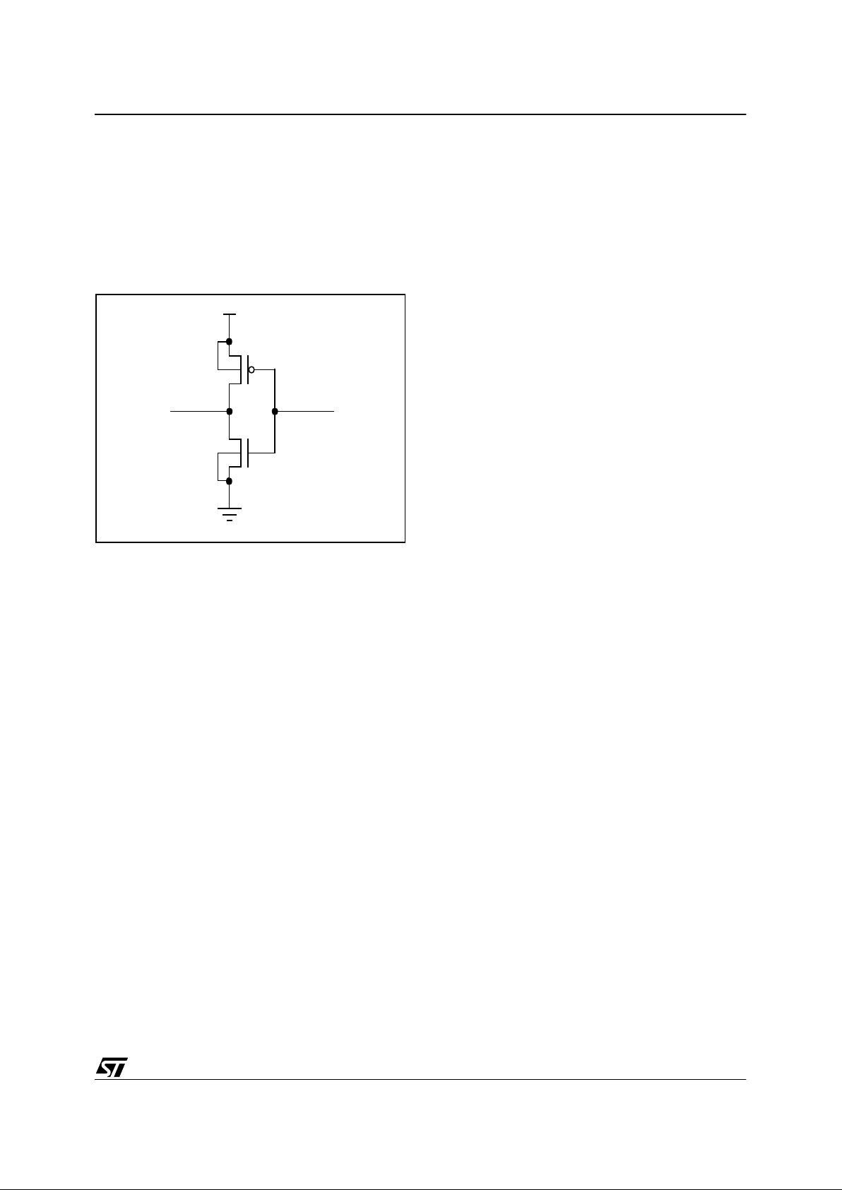
Figure 6. CMOS basic inverter
When an input is kept at logic zero, the N-channel
transistor is off, while the P-channel is on and can
conduct. The opposite occurs when an input is
kept at logic one. CMOS transistors are essentially
linear devices with relatively broad switching
points. During commutation, the input passes
through midsupply, and there is a region of input
voltage values where both P and N-channel transistors are on. Since normally the transitions are
fast, there is a very short time in which a current
can flow: once the s wi tchin g is co mplete d there is
no longer current. This phenomenon explains why
the overall current depends on the switching rate:
the consumption is directly proportional to the
number of transistors inside the device which are
in the linear region during transitions, charging and
discharging internal capacitances.
In order to avoid extra power supply current, it is
important to bias input pins properly when not
used. In fact, if the input impedance is very high,
pins can float, when not connected, either to a
midsupply level or can os cilla te (injecting n oise i n
the device).
Depending on the specific configuration of each
I/O pin on different ST9 devices, it can be more or
less critical to leave un used pins float ing. For this
reason, on most pins, the configuration after RESET enables an internal weak pull-up transistor in
order to avoid floating conditions. For other pins
this is intrinsically forbidden, like for the true open-
drain pins. In any case, the application software
must program the right state for unused pins to
avoid conflicts with ex ternal circuitry (whichev er it
is: pull-up, pull-down, floating, etc.).
The suggested method of termi nating unused I/O
is to connect an external individual pull-up or pulldown for each pin, e ven though initialization sof tware can force outputs to a spec ified and defined
value, during a particular phase of the RESET routine there could be an undetermined status at the
input section.
Usage of pull-ups and/or pull-downs is preferable
in place of direct connection to V
DD
or VSS. If pullup or pull-down resistors are used, inputs can be
forced for test purposes to a different value, and
outputs can be programmed to both digital levels
without generating high current drain due to the
conflict.
Anyway, during system verification flow, attention
must be paid to reviewing the connection of each
pin, in order to avoid potential problems.
1.2. 4 A voidan ce of P i n Damage
Although integrated circuit data sheets provide the
user with conservative limits and conditions in order to prevent damage, sometim es it is useful for
the hardware system designer to know the internal
failure mechanis ms: the risk of expos ure to ille gal
voltages and conditions can be reduced by smart
protection design.
It is not possible to classify and to predict all the
possible damage resulting from violating maximum ratings and conditions, due to the large
number of variables that come into play in defining
the failures: in fact, when an overvoltage condition
is applied, the effects on the device can vary s ignificantly depending on lot-to-lot process variations, operating temperature, e xternal interfacing
of the ST9 with other devices, etc.
In the following sections, background technical information is given in order to help system designers to reduce risk of damage to the ST9 device.
1.2.4.1 Electrostatic Discharge and Latchup
CMOS integrated circuits are generally sensitive
to exposure to high voltage static electricity, which
can induce permanent damage to the device: a
typical failure is the breakdown of thin oxides,
which causes high leakage current and sometimes
shorts.
Latchup is another typical phenomenon occurring
in integrated circuits: unwanted turning on of parasitic bipolar structures, or silicon-controlled rectifi-
P
N
INOUT
V
DD
V
SS
9
Page 12
12/398
ST92F124/F150/F250 - GENER AL DESCRIPTION
ers (SCR), may overheat and rapi dly destroy the
device. These unintentional structures are composed of P and N regions wh ich work as em itters,
bases and collectors of parasitic bipolar transistors: the bulk resistance of the silicon in the wells
and substrate act as resistors on the SCR structure. Applying voltages below V
SS
or above VDD,
and when the level of current is able to generate a
voltage drop across the SCR parasitic resistor, the
SCR m ay be turned o n; to turn of f the SC R it is
necessary to remove the power supply from the
device.
The present ST9 design implements layout and
process solutions to decrease the effec ts of electrostatic discharges (ESD) and la tchup. Of course
it is not possible to test all devices, due to the destructive nature of the mechanism; in order to
guarantee product relia bility, destructi ve tests are
carried out on groups of devices, according to
STMicroelectronics internal Quality Assurance
standards and recommendations.
1.2.4.2 Protective Interface
Although ST9 input/output circuitry has been designed taking ESD and Latchup problems into account, for those applications an d systems where
ST9 pins are exposed to illegal voltages and h igh
current injections, the user is strongly recommended to implement ha rdware s olu tions which reduc e
the risk of damage to the microcontroller: low-pass
filters and clamp diodes are usually sufficient in
preventing stress conditions.
The risk of having out-of-range voltages an d currents is greater for those signals coming from outside the system, where noise effect or uncontrolled spikes could occur with higher probability
than for the internal signals; it must be underlined
that in some cases, adoption of filters or other dedicated interface circuitries might affect global microcontroller performance, inducing undesired timing delays, and impacting the global system
speed.
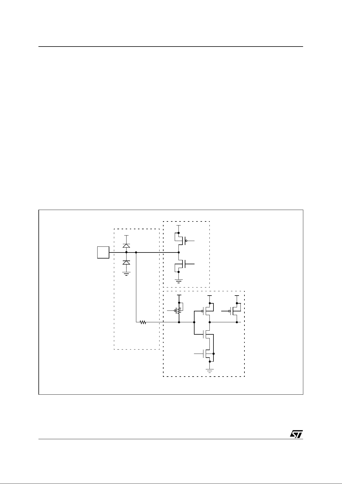
Figure 7. Digital Input/Output - Push-Pull
PIN
OUTPUT
BUFFER
P
N
P
N
N
IN PUT
BUFFER
P
ESD PROTECTION
CIRCUITRY
PORT CIRCUITRY
I/O CIRCUITRY
P
EN
EN
9
Page 13
13/398
ST92F124/F150/F250 - GENER AL DESCRIPTION
1.2.4.3 Internal Circuitry: Digital I/O pin
In Figure 7 a schematic repres entation of an S T9
pin able to operate either as an input or as an output is shown. The circuitry imple men ts a stand ard
input buffer and a push-pull configuration for the
output buffer. It is evident that although it is possible to disable the output buffer when the input section is used, the MOS transistors of the buffer itself
can still affect the behaviour of the pin when exposed to illegal conditions. In f act, the P-channel
transistor of the output buffer implements a direct
diode to V
DD
(P-diffusion of the drain connected to
the pin and N-well connected to V
DD
), while the Nchannel of the output buffer implements a diode to
V
SS
(P-substrate connected to V SS and N-diffusion of the drain connected to the pin). In parallel
to these diodes, dedicated circuitry is implemented
to protect the logic from ESD events (MOS, diodes
and input series resistor).
The most important characteristic of these extra
devices is that they must not disturb normal operating modes, while acting during exposure t o over
limit conditions, avoiding permanent damage to
the logic circuitry.
All I/O pins can generally be programmed to work
also as open-drain outputs, by simply writing in the
corresponding register of the I/O Port. The gate of
the P-channel of t he o utpu t buffer i s disabl ed: it is
important to highlight that physically the P-channel
transistor is still present, so the diode to V
DD
works. In some applications it can occur that the
voltage applied to the pin is higher than the V
DD
value (supposing the external line is kept high,
while the ST9 power supply is turned off): this condition will inject current throug h the diode , risking
permanent damages to the device.
In any case, programming I/O pins as open -drain
can help when several pins in the system are tied
to the same point: of course software must pay attention to program only one of them as output at
any time, to avoid output driver contentions; it is
advisable to configure these pins a s output opendrain in order to reduce the risk of current contentions.
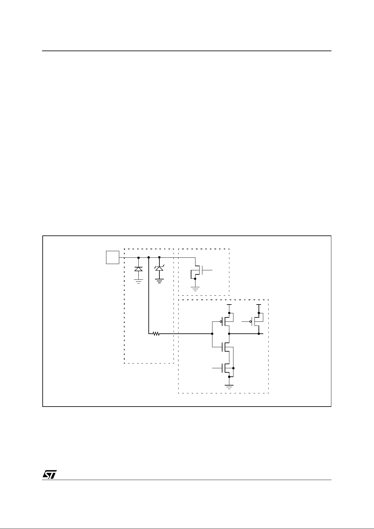
Figure 8. Digital Input/Output - True Open Drain Output
PIN
OUTPUT
BUFFER
N
P
N
N
IN P UT
BUFFER
ESD PROTECTION
CIRCUITRY
PORT CIRCUITRY
I/O CIRCUITRY
P
EN
EN
9
Page 14
14/398
ST92F124/F150/F250 - GENER AL DESCRIPTION
In Figure 8 a true open-drain pin schematic is
shown. In this case all pa ths to V
DD
are removed
(P-channel driver, ESD protection diode, internal
weak pull-up) in order to allow the system to turn
off the power supply of the microcontroller and
keep the voltage level at the pin high without injecting current in the device. This is a typical condition which can occur when several devices interface a serial bus: if one device is not involved in
the communication, it can be disabled by turning
off its power supply to reduce the system current
consumption.
When an illegal negative voltage level is appl ied to
the ST9 I/O pins (both versions, push-pull and true
open-drain output) the clamp diode is always
present and active (see ESD protection circuitry
and N-channel driver).
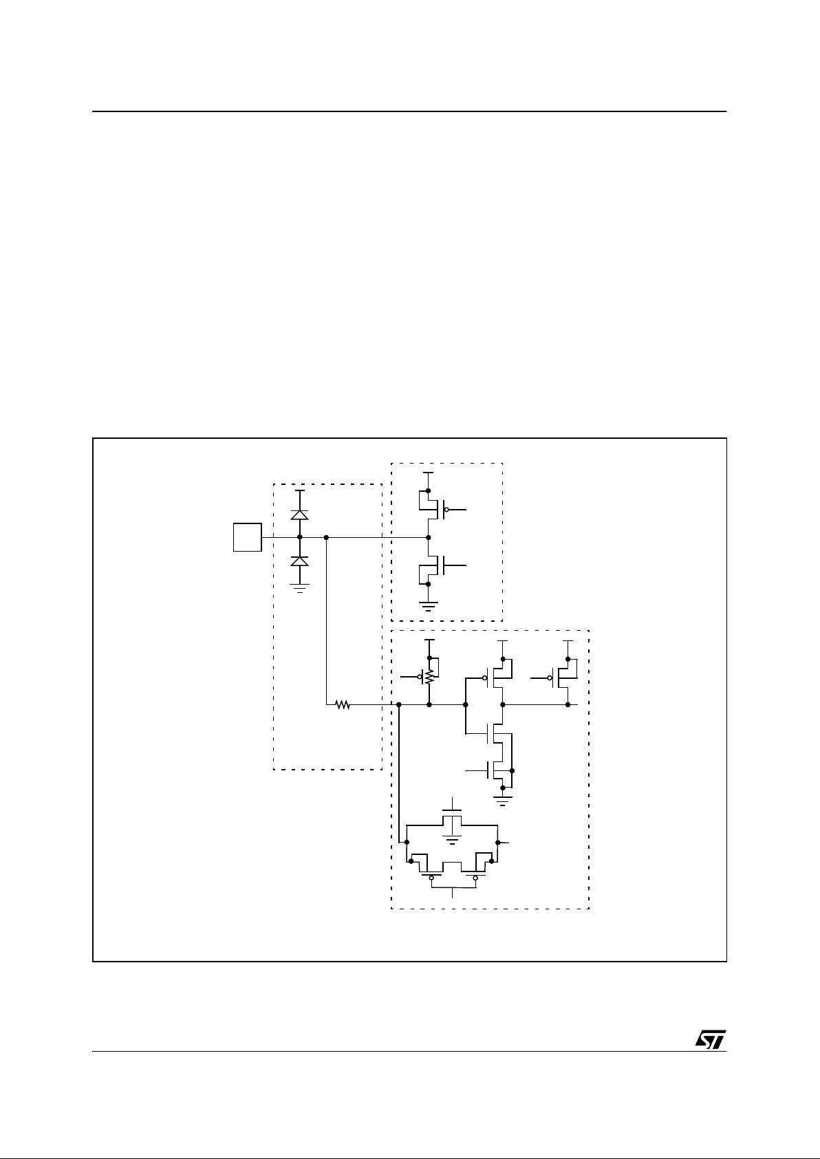
1.2.4.4 Internal Circuitry: Analog Input pin
Figure 9 shows the internal circuitry used for ana-
log input. It is substantially a digital I/O with an
added analog multipl exer for the selection of the
input channel of the Analog to Digital Converter
(ADC).
The presence of the multiplexer P-channel and Nchannel can affect the behaviour of the pin when
exposed to ille gal voltage condi tions. These transistors are controlled by a low noise logic, biased
through AV
DD
and AVSS including P-channel Nwell: it is important t o always verify the i nput vol tage value with respect to both analog power supply and digital power supply, in order to avoi d unintended current injections which (if not limited)
could destroy the device.
Figure 9. Digital Input/Output - Push-Pull Output - Analog Multiplexer Input
PIN
OUTPUT
BUFFER
P
N
P
N
N
INP UT
BUFFER
P
E
SD PROTECTION
CIRCUITRY
PORT CIRCUITRY
I/O CIRC UIT RY
P
EN
EN
N
P
P
9
Page 15

15/398
ST92F124/F150/F250 - GENER AL DESCRIPTION
1.2.4.5 Power Supply and Ground
As already said for the I/O pins, in order to guarantee ST9 compliancy with respect to Quality Assu rance recommendations concerning ESD and
Latchup, dedicated circuits are added to the different power supply and ground pins (digital and analog). These structures create preferred paths for
the high current injected during discharges, avoiding damage to active logic and circuitry. It is important for the system designer to take this added circuitry into account, which is not always t ransparent with respect to the relative level of voltages applied to the different power supply and ground
pins. Figure 10 shows schematically the protection
net implemented on ST9 devices, composed of diodes and other special structures.
The clamp structure between the V
DD
and V
SS
pins is designed to be active during very fast tran-
sitions (typical of electrostat ic discharges). Other
paths are implemented throu gh diodes: they limit
the possibility of positively differentiating AV
DD
and VDD (i.e. AVDD > VDD); similar considerations
are valid for AV
SS
and VSS due to the back-toback diode structure implemented between the
two pins. Anyw ay, it mus t be highlighted t hat, because V
SS
and AVSS are connected to the substrate of the silicon die (even though in different areas of the die itself), they represent the reference
point from which all other voltages are measured,
and it is recommended to never differentiate AV
SS
from VSS.
Note: If more than one pair of pins for V
SS
and
V
DD
is available on the device, they are connected
internally and the protec tion net diagram rem ains
the same as shown in Figure 10.
Figure 10. P ower Supply an d Gro und Configurat i on
N
P
P
N
V
DD
V
SS
AV
DD
AV
SS
V
TEST
9
Page 16

16/398
ST92F124/F150/F250 - GENER AL DESCRIPTION
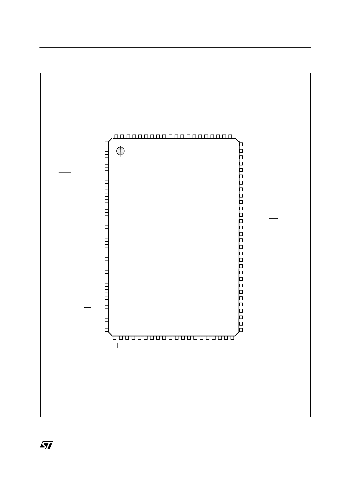
Figure 11. ST92F124/S T92 F150: Pin Configuration (Top-view TQ FP64)
TX0*/WAIT/WKUP5/P5.0
RX0*/WKU P6/WDOUT/P5.1
SIN/WKUP2 /P5.2
WDIN/SOUT /P5.3
TXCLK/CLKOUT /P5.4
RXCL0/WKUP7 /P5.5
DCD/WKUP8 /P5.6
WKUP9/RTS /P5.7
WKUP4/P4.4
EXTRG/STOUT /P4.5
SDA/P4.6
WKUP1/SCL /P4.7
S
S/P3.4
MISO/P3.5
MOSI/P3.6
SCK/WKUP0 /P3.7
HW0SW1
RESET
OSCOUT
OSCIN
VDDVSSP7.7/AIN15 /WKUP13
P7.6/AIN14 /WKUP12
P7.5/AIN13 /WKUP11
P7.4/AIN12 /WKUP3
P7.3/AIN11
P7.2/AIN10
P7.1/AIN9
P7.0/AIN8
/
CK_AF
AV
SSAVDD
N.C
P6.5/WKUP1 0/INTCLK
P6.4/NMI
P6.3/INT3/IN T5
P6.2/INT2/IN T4
P6.0/INT0/IN T1/CLOCK2/8
P0.7
P0.6
P0.5
P0.4
P0.3
P0.2
P0.1
P0.0
Reserved**
Reserved**
Reserved**
TINPA0/P2.0
TINPB0/P2.1
TOUTA0/P2.2
TOUTB0/P2.3
TINPA1/P2.4
TINPB1/P2.5
TOUTA1/P2.6
TOUTB1/P2.7
V
SS
V
DD
V
REG
V
TEST
P1.0
P1.1
P1.2
6463 62616059 58 57 56 55545352515049
48
47
46
45
44
43
42
41
40
39
38
37
36
35
34
33
1718192021222324 2930 31 3225262728
1
2
3
4
5
6
7
8
9
10
11
12
13
14
15
16
ST92F124 /
* Not available on ST92F124 version
ST92F150
1718192021222324 2930 31 3225262728
* * Reserved for ST tests, must be left unconnected
9
Page 17
17/398
ST92F124/F150/F250 - GENER AL DESCRIPTION
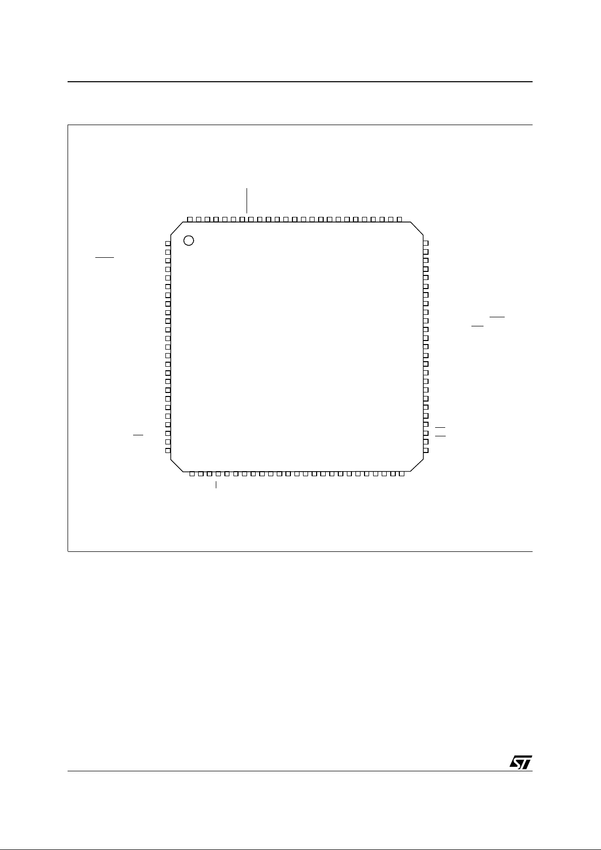
Figure 12. ST92F150: Pin Configuration (Top-view PQFP100)
A17/P9.3
A18/P9.4
A19/P9.5
A20/P9.6
A21/P9.7
TX0/WAIT
/WKUP5/P5 .0
RX0/WKUP6/ WDOUT/P5.1
SIN/WKUP2/P5 .2
WDIN/SOUT/P5 .3
TXCLK/CLKO UT/P5.4
RXCLK/WKU P7/P5.5
DCD/WKUP8/P5 .6
WKUP9/RTS/P5 .7
ICAPA1/P4.0
CLOCK2/P4 .1
OCMPA1/P4 .2
V
SS
V
DD
ICAPB1/OCMP B1/P4.3
EXTCLK1/WKU P4/P4.4
EXTRG/STO UT/P4.5
SDA/P4.6
WKUP1/SCL/P4 .7
ICAPB0/P3.1
ICAPA0/OCMP A0/P3.2
OCMPB0/P3 .3
EXTCLK0/S S
/P3.4
MISO/P3.5
MOSI/P3.6
SCK/WKUP0/P3 .7
P9.2/A16
P9.1/TDO
P9.0/RDI
HW0SW1
RESET
OSCOUT
OSCIN
VDDVSSP7.7/AIN15/7/W KUP13
P7.6/AIN14/WK UP12
P7.5/AIN13/WK UP11
P7.4/AIN12/WK UP3
P7.3/AIN11
P7.2/AIN10
P7.1/AIN9
P7.0/AIN8
/
CK_AF
AV
SSAVDD
P8.7/AIN7
P8.6/AIN6
P8.5/AIN5
P8.4/AIN4
P8.3/AIN3
P8.2/AIN2
P8.1/AIN1/WKU P15
P8.0/AIN0/WKU P14
VPWO*
P6.5/WKUP10/I NTCLK/VPW
P6.4/NMI
P6.3/INT3/INT5
P6.2/INT2/INT4 /DS2
P6.1/INT6/RW
P6.0/INT0/INT1 /CLOCK2/8
P0.7/A7/D7
V
DD
V
SS
P0.6/A6/D6
P0.5/A5/D5
P0.4/A4/D4
P0.3/A3/D3
P0.2/A2/D2
P0.1/A1/D1
P0.0/A0/D0
AS
DS
P1.7/A15
P1.6/A14
P1.5/A13
P1.4/A12
V
REG
RW
TINPA0/P2.0
TINPB0/P2.1
TOUTA0/P2.2
TOUTB0/P2.3
TINPA1/P2.4
TINPB1/P2.5
TOUTA1/P2.6
TOUTB1/P2.7
V
SS
V
DD
V
REG
V
TEST
A8/P1.0
A9/P1.1
A10/P1.2
A11/P1.3
**RX1/WKUP6
**TX1
1
50
30
ST92F150
2
3
4
5
6
7
8
9
10
11
12
13
14
15
16
17
18
19
20
21
22
23
24
25
26
27
28
29
80
51
79
78
77
76
75
74
73
72
71
70
69
68
67
66
65
64
63
62
61
60
59
58
57
56
55
54
53
52
49484746454443424140393837363534333231
81
828384858687888990919293
94
9596979899100
*On devices without JPBLD peripheral, this pin must not be connected.
**On devices without CAN1 peripheral, these pins must not be connected.
9
Page 18
18/398
ST92F124/F150/F250 - GENER AL DESCRIPTION
Figure 13. ST92F150: Pin Configuration (Top-view TQ FP100)
* V
TEST
must be kept low in standard operating mode.
**On devices without CAN1 peripheral, these pins must not be connected.
1
2
3
4
5
6
7
8
9
10
11
12
13
14
15
16
17
18
19
20
21
22
23
24
25
26
2728 29 3031 3233 343536 3738 39 4041 4243 4445 46 4748 4950
75
74
73
72
71
70
69
68
67
66
65
64
63
62
61
60
59
58
57
56
55
54
53
52
51
10099 98 9796 9594 9392 91 9089 8887 868584 8382 81 8079 7877 76
ST92F150
P8.4/AIN4
P8.3/AIN3
P8.2/AIN2
P8.1/AIN1/WKUP15
P8.0/AIN0/WKUP14
VPWO
P6.5/WKUP10/INTCLK/VPW
P6.4/NMI
P6.3/INT3/INT5
P6.2/INT2/INT4/DS2
P6.1/INT6/RW
P6.0/INT0/INT1/CLOCK2/8
P0.7/A7/D7
V
DD
V
SS
P0.6/A6/D6
P0.5/A5/D5
P0.3/A3/D3
P0.2/A2/D2
P0.1/A1/D1
P0.0/A0/D0
AS
DS
P0.4/A4/D4
P1.7/A15
A20/P9.6
TX0/WAIT
/WKUP5/P5.0
RX0/WKUP6/WDOUT/P5.1
TXCLK/CLKOUT/P5.4
OCMPA1/P4.2
V
DD
A21/P9.7
WDIN/SOUT/P5.3
DCD/WKUP8/P5.6
V
SS
ICAPB1/OCMPB1/P4.3
SDA/P4.6
SIN/WKUP2/P5.2
RXCLK/WKUP7/P5.5
CLOCK2/P4.1
EXTCLK1/WKUP4/P4.4
ICAPB0/P3.1
ICAPA0/OCMPA0/P3.2
WKUP9/RTS/P5.7
ICAPA1/P4.0
EXTRG/STOUT/P4.5
WKUP1/SCL/P4.7
OCMPB0/P3.3
EXTCLK0/SS
/P3.4
MISO/P3.5
P9.5/A19
P9.4/A18
P9.2/A16
HW0SW1
P7.7/AIN15/7/WKUP13
P7.4/AIN12/WKUP3
P9.3/A17
P9.0/RDI
RESET
P7.6/AIN14/WKUP12
P7.5/AIN13/WKUP11
P7.1/AIN9
P9.1/TDO
OSCIN
V
SS
P7.3/AIN11
P7.0/AIN8/CK_AF
P8.7/AIN7
OSCOUT
V
DD
P7.2/AIN10
AVSSAVDDP8.6/AIN6
P8.5/AIN5
MOSI/P3.6
SCK/WKUP0/P3.7
RW
TOUTA0/P2.2
V
SS
*V
TEST
V
REG
TINPB0/P2.1
TOUTB0/P2.3
V
DD
V
REG
A10/P1.2
TINPA0/P2.0
TINPB1/P2.5
TOUTB1/P2.7
A8/P1.0
A11/P1.3
A12/P1.4
TINPA1/P2.4
TOUTA1/P2.6
A9/P1.1
**RX1/WKUP6
**TX1
A13/P1.5
A14/P1.6
9
Page 19

19/398
ST92F124/F150/F250 - GENER AL DESCRIPTION
Figure 14. ST92F250: Pin Configuration (Top-view PQFP100)
* V
TEST
must be kept low in standard operating mode.
SDA1/A17/P9.3
SCL1/A18/P9.4
A19/P9.5
A20/P9.6
A21/P9.7
TX0/WAIT
/WKUP5/P5.0
RX0/WKUP6/WDOUT/P5.1
SIN/WKUP2/P5.2
WDIN/SOUT/P5.3
TXCLK/CLKOUT/P5.4
RXCLK/WKUP7/P5.5
DCD/WKUP8/P5.6
WKUP9/RTS/P5.7
ICAPA1/P4.0
CLOCK2/P4.1
OCMPA1/P4.2
V
SS
V
DD
ICAPB1/OCMPB1/P4.3
EXTCLK1/WKUP4/P4.4
EXTRG/STOUT/P4.5
SDA0/P4.6
WKUP1/SCL0/P4.7
ICAPB0/P3.1
ICAPA0/OCMPA0/P3.2
OCMPB0/P3.3
EXTCLK0/SS
/P3.4
MISO/P3.5
MOSI/P3.6
SCK/WKUP0/P3.7
P9.2/A16
P9.1/TDO
P9.0/RDI
HW0SW1
RESET
OSCOUT
OSCIN
VDDVSSP7.7/AIN15/7/WKUP13
P7.6/AIN14/WKUP12
P7.5/AIN13/WKUP11
P7.4/AIN12/WKUP3
P7.3/AIN11
P7.2/AIN10
P7.1/AIN9
P7.0/AIN8/CK_AF
AVSSAVDDP8.7/AIN7
P8.6/AIN6
P8.5/AIN5
P8.4/AIN4
P8.3/AIN3
P8.2/AIN2
P8.1/AIN1/WKUP15
P8.0/AIN0/WKUP14
P3.0
P6.5/WKUP10/INTCLK
P6.4/NMI
P6.3/INT3/INT5
P6.2/INT2/INT4/DS2
P6.1/INT6/RW
P6.0/INT0/INT1/CLOCK2/8
P0.7/A7/D7
V
DD
V
SS
P0.6/A6/D6
P0.5/A5/D5
P0.4/A4/D4
P0.3/A3/D3
P0.2/A2/D2
P0.1/A1/D1
P0.0/A0/D0
AS
DS
P1.7/A15
P1.6/A14
P1.5/A13
P1.4/A12
V
REG
RW
TINPA0/P2.0
TINPB0/P2.1
TOUTA0/P2.2
TOUTB0/P2.3
TINPA1/P2.4
TINPB1/P2.5
TOUTA1/P2.6
TOUTB1/P2.7
V
SS
V
DD
V
REG
*V
TEST
A8/P1.0
A9/P1.1
A10/P1.2
A11/P1.3
P6.6
P6.7
1
50
30
ST92F250
2
3
4
5
6
7
8
9
10
11
12
13
14
15
16
17
18
19
20
21
22
23
24
25
26
27
28
29
80
51
79
78
77
76
75
74
73
72
71
70
69
68
67
66
65
64
63
62
61
60
59
58
57
56
55
54
53
52
49484746454443424140393837363534333231
81
828384858687888990919293949596979899100
9
Page 20

20/398
ST92F124/F150/F250 - GENER AL DESCRIPTION
Figure 15. ST92F250: Pin Configuration (Top-view TQ FP100)
* V
TEST
must be kept low in standard operating mode.
1
2
3
4
5
6
7
8
9
10
11
12
13
14
15
16
17
18
19
20
21
22
23
24
25
26
2728 29 3031 3233 3435 36 3738 3940 4142 43 4445 4647 48 49 50
75
74
73
72
71
70
69
68
67
66
65
64
63
62
61
60
59
58
57
56
55
54
53
52
51
10099 98 97 96 9594 9392 91 9089 8887 8685 84 8382 8180 7978 7776
ST92F250
P8.4/AIN4
P8.3/AIN3
P8.2/AIN2
P8.1/AIN1/WKUP15
P8.0/AIN0/WKUP14
P3.0
P6.5/WKUP10/INTCLK
P6.4/NMI
P6.3/INT3/INT5
P6.2/INT2/INT4/DS2
P6.1/INT6/RW
P6.0/INT0/INT1/CLOCK2/8
P0.7/A7/D7
V
DD
V
SS
P0.6/A6/D6
P0.5/A5/D5
P0.3/A3/D3
P0.2/A2/D2
P0.1/A1/D1
P0.0/A0/D0
AS
DS
P0.4/A4/D4
P1.7/A15
A20/P9.6
TX/WAIT
/WKUP5/P5.0
RX/WKUP6/WDOUT/P5.1
TXCLK/CLKOUT/P5.4
OCMPA1/P4.2
V
DD
A21/P9.7
WDIN/SOUT/P5.3
DCD/WKUP8/P5.6
V
SS
ICAPB1/OCMPB1/P4.3
SDA0/P4.6
SIN/WKUP2/P5.2
RXCLK/WKUP7/P5.5
CLOCK2/P4.1
EXTCLK1/WKUP4/P4.4
ICAPB0/P3.1
ICAPA0/OCMPA0/P3.2
WKUP9/RTS/P5.7
ICAPA1/P4.0
EXTRG/STOUT/P4.5
WKUP1/SCL0/P4.7
OCMPB0/P3.3
EXTCLK0/SS
/P3.4
MISO/P3.5
P9.5/A19
P9.4/A18/SCL1
P9.2/A16
HW0SW1
P7.7/AIN15/7/WKUP13
P7.4/AIN12/WKUP3
P9.3/A17/SDA1
P9.0/RDI
RESET
P7.6/AIN14/WKUP12
P7.5/AIN13/WKUP11
P7.1/AIN9
P9.1/TDO
OSCIN
V
SS
P7.3/AIN11
P7.0/AIN8/CK_AF
P8.7/AIN7
OSCOUT
V
DD
P7.2/AIN10
AVSSAVDDP8.6/AIN6
P8.5/AIN5
MOSI/P3.6
SCK/WKUP0/P3.7
RW
TOUTA0/P2.2
V
SS
*V
TEST
V
REG
TINPB0/P2.1
TOUTB0/P2.3
V
DD
V
REG
A10/P1.2
TINPA0/P2.0
TINPB1/P2.5
TOUTB1/P2.7
A8/P1.0
A11/P1.3
A12/P1.4
TINPA1/P2.4
TOUTA1/P2.6
A9/P1.1
P6.6
P6.7
A13/P1.5
A14/P1.6
9
Page 21
21/398
ST92F124/F150/F250 - GENER AL DESCRIPTION
Table 1. ST92F124/F 150/F250 Power Supply Pins
Table 2. ST92F124/F150/F250 Primary Function Pins
Note 1: ST92F150JDV1 only.
Name Function TQFP64 P QFP100 TQFP100
V
DD
Main Power Supply Voltage
(Pins internally connected)
-1815
27 42 39
-6562
60 93 90
V
SS
Digital Circuit Ground
(Pins internally connected)
-1714
26 41 38
-6461
59 92 89
AV
DD
Analog Circuit Supply Voltage 49 82 79
AV
SS
Analog Circuit Ground 50 83 80
V
TEST
Must be kept low in standard operating mode 29 44 41
V
REG
Stabilization capacitor(s) for internal voltage regulator 28
31
43
28
40
Name Function TQFP64 PQFP100 TQFP100
AS
Address Strobe - 56 53
DS
Data Strobe - 55 52
RW
Read/Write - 32 29
OSCIN Crystal Oscillator Input 61 94 91
OSCOUT Crystal Oscillator Output 62 95 92
RESET
Reset to initialize the Microcontroller 63 96 93
HW0SW1 Watchdog HW/SW enabling selection 64 97 94
VPWO
1)
J1850 JBLPD Output - 73 70
RX1/WKUP6
1)
CAN1 Receive Data / Wake-up Line 6 - 49 46
TX1
1)
CAN1 Transmit Data. - 50 47
9
Page 22
22/398
ST92F124/F150/F250 - GENER AL DESCRIPTION
1.3 VOLTAGE REGULATOR
The internal Voltage Regulator (VR) is used to
power the microcontroller starting from the external power supply. The VR comprises a M ain voltage regulator and a Low-power regulator.
– The Mai n voltage regulator generates sufficient
current for the microcontroller to operate in any
mode. It has a static power consum ption (300
µA typ.).
– The separate Low-Power regulator consumes
less power is used only wh en t he m icrocont roller is in Low Power mode. It has a different design from the main VR a nd generates a lower,
non-stabilized and non- ther m ally- com pens at ed
voltage sufficient for maintaining the data in
RAM and the Register File.
For both the Main VR and the Low-Power VR, stabilization is achieved by an external capacitor,
connected to on e of the V
REG
pins. The minimum
recommended value is 300 nF, and care must be
taken to minimize distance between the chip and
the capacitor. Care should also be taken to limit
the serial inductance to less than 60nH.
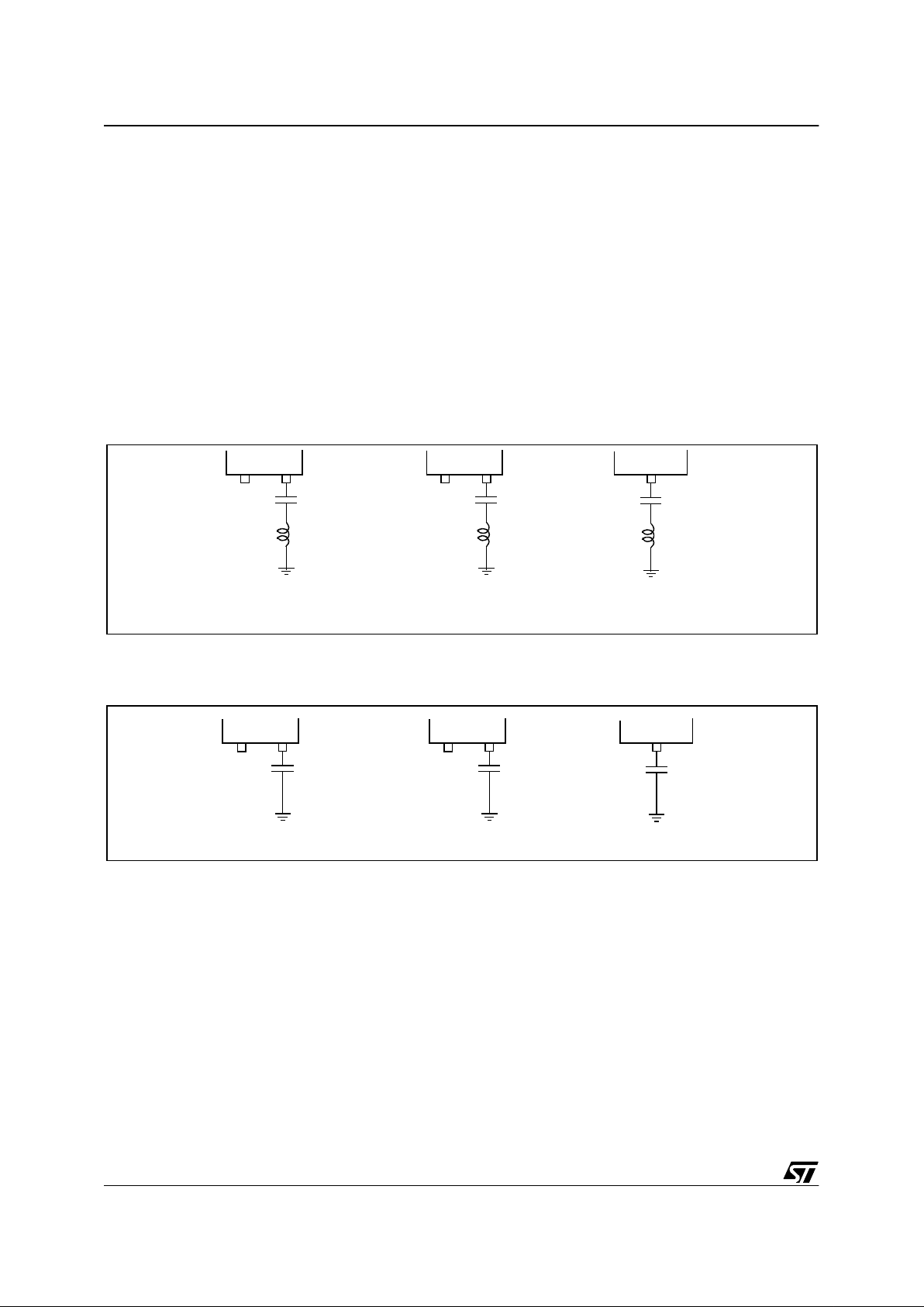
Figure 16. Recommended Connections for V
REG
IMPORTANT: The V
REG
pin cannot be used to drive external devices.
Figure 17. Minimum Required Connections for V
REG
Note: Pin 31 of PQFP100 or pin 28 of TQFP100 can be left unconnnected. A secondary stabilization net-
work can also be connected to these pins.
PQFP100
QFP64
C
L
L = Ferrite bead for EMI protection.
Pin 28
C
L
Pin 43
Pin 31
TQFP100
C
L
Pin 40
Pin 28
Suggested type: Murata BLM18BE601FH1: (Imp. 600 Ω at 100 M Hz).
C = 300 to 600nF
C
PQFP100 QFP64
C
Pin 43Pin 31 Pin 28
C
TQFP100
Pin 40Pin 28
C = 300 to 600nF
9
Page 23

23/398
ST92F124/F150/F250 - GENER AL DESCRIPTION
1.4 I/O PORTS
Port 0, Port 1 and Port 9[7:2] provide the external
memory interface. All the ports of the device ca n
be programmed as Inp ut/Output or i n I nput m ode,
compatible with TTL or CMOS levels (except
where Schmitt Trigger is present). Each bit can be
programmed individually (Refer to the I/O ports
chapter).
Internal Weak Pull-up
As shown in Table 3, not all input sections imple-
ment a Weak P ull-up. Thi s m eans that t he pull -up
must be connected externally when the p in is not
used or programmed as bidirectional.
TTL/CMO S I np ut
For all those port bits where no input schmitt trigger is implemented, it is always possible to program the input level as TTL or CMOS compatible
by programming the relevant PxC2.n control bit.
Refer I/O Ports Chapter to the section titled “Input/
Output Bit Configuration”.
Schmitt Tr ig ger I nput
Two different kinds of Schmitt Trigger circuitries
are implemented: Standard and High Hysteresis.
Standard Schmitt Trigger is w idely used (see Ta-
ble 3), while the High Hysteresis Schmitt Trigger is
present on ports P4[7:6] and P6[5:4].
All inputs which can be used for detecting interrupt
events have been configured with a “Standard”
Schmitt Trigger, apart from the NMI pin which i mplements the “High Hysteresis” version. In this
way, all interrupt lines are guaranteed as “level
sensitive”.
Push-Pull/OD Output
The output buffer can be programmed as pushpull or open-drain: attention must be paid to the
fact that the open-drain option corresponds only to
a disabling of P-channel MOS transistor of the
buffer itself: it is still present and physically connected to the pin. Consequently it is not possible to
increase the output voltage on the pin over
V
DD
+0.3 Volt, to avoid direct junction biasing.
Pure Open-Drain Output
The user can increase t he voltage on an I/O pin
over V
DD
+0.3 Volt where the P-channel MOS transistor is physically absent: this is allowed on all
“Pure Open Drain” pins. In this case, the push-pull
option is not available and a ny weak pull-up m ust
be implemented externally.
Table 3. I/O Port Characteristics
Legend: WPU = Weak Pull-Up, OD = Open Drain.
Note 1: Port 3.0 and Port6 [7:6] present on ST92F250 version only.
Input Output Weak Pull-Up Reset State
Port 0[7:0] TTL/CMOS Push-Pull/OD No Bidirectional
Port 1[7:0] TTL/CMOS Push-Pull/OD No Bidirectional
Port 2[1:0]
Port 2[3:2]
Port 2[5:4]
Port 2[7:6]
Schmitt trigger
TTL/CMOS
Schmitt trigger
TTL/CMOS
Push-Pull/OD
Pure OD
Push-Pull/OD
Push-Pull/OD
Yes
No
Yes
Yes
Input
Input CMOS
Input
Input CMOS
Port 3[2:0]
1)
Port 3.3
Port 3[7:4]
Schmitt trigger
TTL/CMOS
Schmitt trigger
Push-Pull/OD
Push-Pull/OD
Push-Pull/OD
Yes
Yes
Yes
Input
Input CMOS
Input
Port 4.0, Port 4.4
Port 4.1
Port 4.2, Port 4.5
Port 4.3
Port 4[7:6]
Schmitt trigger
Schmitt trigger
TTL/CMOS
Schmitt trigger
High hysteresis Schmitt trigger
Push-Pull/OD
Push-Pull/OD
Push-Pull/OD
Push-Pull/OD
Pure OD
No
Yes
Yes
Yes
No
Input
Bidirectional WPU
Input CMOS
Input
Input
Port 5[2:0], Port 5[7:4]
Port 5.3
Schmitt trigger
TTL/CMOS
Push-Pull/OD
Push-Pull/OD
No
Yes
Input
Input CMOS
Port 6[3:0]
Port 6[5:4]
Port 6[7:6]
1)
Schmitt trigger
High hysteresis Schmitt trigger
Schmitt trigger
Push-Pull/OD
Push-Pull/OD
Push-Pull/OD
Yes
Yes
Yes
Input
Input
Input
Port 7[7:0] Schmitt trigger Push-Pull/OD Yes Input
Port 8[1:0]
Port 8[7:2]
Schmitt trigger
Schmitt trigger
Push-Pull/OD
Push-Pull/OD
Yes
Yes
Input
Bidirectional WPU
Port 9[7:0] Schmitt trigger Push-Pull/OD Yes Bidirectional WPU
9
Page 24

24/398
ST92F124/F150/F250 - GENER AL DESCRIPTION
How to Configure the I/O Ports
To configure the I/O ports, use the information in
Table 3, Table 4 and the Port Bit Configuration Ta-
ble in the I/O Ports Chapter (See page 149).
Input Note = the hardware characteristics fixed for
each port line in Table 3.
– If Input note = TTL/CMOS, either TTL or CMOS
input level can be selected by software.
– If Input note = Schmitt trigger, selecting CMOS
or TTL input by software has no effect, the input
will always be Schmit t Trigger.
Alternate Functions (AF) = More than one AF
cannot be assigned to an I/O pin at the same time:
An alternate function can be selected as follows.
AF Inputs:
– AF is selected implicitly by enabling the corre-
sponding peripheral. Exception to this are ADC
inputs which must be explicitly selected as AF in-
put by software.
AF Outputs or Bidirectional Lines:
– In the case of Outputs or I/Os, AF is selected ex-
plicitly by sof twar e.
Example 1: SCI-M input
AF: SIN, Port: P5.2. Schmitt Trigger input.
Write the port configuration bits:
P5C2.2=1
P5C1.2=0
P5C0.2 =1
Enable the SCI peripheral by software as described in the SCI chapter.
Example 2: SCI-M output
AF: SOUT, Port: P5.3, Push-Pull/OD output.
Write the port configuration bits (for AF OUT PP):
P5C2.3=0
P5C1.3=1
P5C0.3 =1
Example 3: External Memory I/O
AF: A0/D0, Port : P0.0, Input Note: TTL/CMOS in-
put.
Write the port configuration bits:
P0C2.0=1
P0C1.0=1
P0C0.0 =1
Example 4: Analog input
AF: AIN8, Port : 7.0, Analog input.
Write the port configuration bits:
P7C2.0=1
P7C1.0=1
P7C0.0 =1
9
Page 25

25/398
ST92F124/F150/F250 - GENER AL DESCRIPTION
1.5 Alternat e Functions for I/O Ports
All the ports in the following table are useable for general purpose I/O (input, output or bidirectional).
Table 4. I/O Port Alternate Functions
Port
Name
Pin No.
Alternate Functions
TQFP64 PQFP100 TQFP100
P0.0 - 57 54 A0/D0 I/O Address/Data bit 0
P0.1 - 58 55 A1/D1 I/O Address/Data bit 1
P0.2 - 59 56 A2/D2 I/O Address/Data bit 2
P0.3 - 60 57 A3/D3 I/O Address/Data bit 3
P0.4 - 61 58 A4/D4 I/O Address/Data bit 4
P0.5 - 62 59 A5/D5 I/O Address/Data bit 5
P0.6 - 63 60 A6/D6 I/O Address/Data bit 6
P0.7 - 66 63 A7/D7 I/O Address/Data bit 7
P1.0 - 45 42 A8 I/O Address bit 8
P1.1 - 46 43 A9 I/O Address bit 9
P1.2 - 47 44 A10 I/O Address bit 10
P1.3 - 48 45 A11 I/O Address bit 11
P1.4 - 51 48 A12 I/O Address bit 12
P1.5 - 52 49 A13 I/O Address bit 13
P1.6 - 53 50 A14 I/O Address bit 14
P1.7 - 54 51 A15 I/O Address bit 15
P2.0 18 33 30 TINPA0 I Multifunction Timer 0 - Input A
P2.1 19 34 31 TINPB0 I Multifunction Timer 0 - Input B
P2.2 20 35 32 TOUTA0 O Multifunction Timer 0 - Output A
P2.3 21 36 33 TOUTB0 O Multifunction Timer 0 - Output B
P2.4 22 37 34 TINPA1 I Multifunction Timer 1 - Input A
P2.5 23 38 35 TINPB1 I Multifunction Timer 1 - Input B
P2.6 24 39 36 TOUTA1 O Multifunction Timer 1 - Output A
P2.7 25 40 37 TOUTB1 O Multifunction Timer 1 - Output B
P3.0
1)
-7370
P3.1 - 24 21 ICAPB0 I Ext. Timer 0 - Input Capture B
P3.2 - 25 22
ICAPA0 I Ext. Timer 0 - Input Capture A
OCMPA0 O Ext. Timer 0 - Output Compare A
P3.3 - 26 23 OCMPB0 O Ext. Timer 0 - Output Compare B
P3.4 - 27 24
EXTCLK0 I Ext. Timer 0 - Input Clock
SS I SPI - Slave Select
P3.5 14 28 25 MISO I/O SPI - Master Input/Slave Output Data
P3.6 15 29 26 MOSI I/O SPI - Master Output/Slave Input Data
9
Page 26

26/398
ST92F124/F150/F250 - GENER AL DESCRIPTION
P3.7 16 30 27
SCK I SPI - Serial Input Clock
WKUP0 I Wake-up Line 0
SCK O SPI - Serial Output Clock
P4.0 - 14 11 ICAPA1 I Ext. Timer 1 - Input Capture A
P4.1 - 15 12 CLOCK2 O CLOCK2 internal signal
P4.2 - 16 13 OCMPA1 O Ext. Timer 1 - Output Compare A
P4.3 - 19 16
ICAPB1 I Ext. Timer 1 - Input Capture B
OCMPB1 O Ext. Timer 1 - Output Compare B
P4.4 - 20 17
EXTCLK1 I Ext. Timer 1 - Input Clock
WKUP4 I Wake-up Line 4
P4.5 10 21 18
EXTRG I ADC Ext. Trigger
STOUT O Standard Timer Output
P4.6 11 22 19 SDA0 I/O I
2
C 0 Data
P4.7 12 23 2 0
WKUP1 I Wake-up Line 1
SCL0 I/O I
2
C 0 Clock
P5.0 1 6 3
WAIT
I External Wait Request
WKUP5 I Wake-up Line 5
TX0
1)
O CAN 0 output
P5.1 2 7 4
WKUP6 I Wake-up Line 6
RX0
1)
I CAN 0 input
WDOUT O Watchdog Timer Output
P5.2 3 8 5
SIN0 I SCI-M - Serial Data Input
WKUP2 I Wake-up Line 2
P5.3 4 9 6
WDIN I Watchdog Timer Input
SOUT O SCI-M - Serial Data Output
P5.4 5 10 7
TXCLK I SCI-M - Transmit Clock Input
CLKOUT O SCI-M - Clock Output
P5.5 6 11 8
RXCLK I SCI-M - Receive Clock Input
WKUP7 I Wake-up Line 7
P5.6 7 12 9
DCD I SCI-M - Data Carrier Detect
WKUP8 I Wake-up Line 8
P5.7 8 13 10
WKUP9 I Wake-up Line 9
RTS O SCI-M - Request To Send
P6.0 43 67 64
INT0 I Ext ernal Interr upt 0
INT1 I Ext ernal Interr upt 1
CLOCK2/8 O CLOCK2 divided by 8
P6.1 - 68 65
INT6 I Ext ernal Interr upt 6
RW
O Read/Wr ite
Port
Name
Pin No.
Alternate Functions
TQFP64 PQFP100 TQFP100
9
Page 27

27/398
ST92F124/F150/F250 - GENER AL DESCRIPTION
P6.2 44 69 66
INT2 I Ext ernal Interr upt 2
INT4 I Ext ernal Interr upt 4
DS2 O Data Strobe 2
P6.3 45 70 67
INT3 I Ext ernal Interr upt 3
INT5 I Ext ernal Interr upt 5
P6.4 46 71 68 NMI I Non Maskable Interrupt
P6.5 47 72 69
WKUP10 I Wake-up Line 10
VPWI
1)
I JBLPD input
INTCLK O Internal Main Clock
P6.6
1)
-4946
P6.7
1)
-5047
P7.0 51 84 81
AIN8 I Analog Data Input 8
CK_AF I Clock Alternative Source
P7.1 52 85 82 AIN9 I Analog Data Input 9
P7.2 53 86 83 AIN10 I Analog Data Input 10
P7.3 54 87 84 AIN11 I Analog Data Input 11
P7.4 55 88 85
WKUP3 I Wake-up Line 3
AIN12 I Analog Data Input 12
P7.5 56 89 86
AIN13 I Analog Data Input 13
WKUP11 I Wake-up Line 11
P7.6 57 90 87
AIN14 I Analog Data Input14
WKUP12 I Wake-up Line 12
P7.7 58 91 88
AIN15 I Analog Data Input 15
WKUP13 I Wake-up Line 13
P8.0 - 74 71
AIN0 I Analog Data Input 0
WKUP14 I Wake-up Line 14
P8.1 - 75 72
AIN1 I Analog Data Input 1
WKUP15 I Wake-up Line 15
P8.2 - 76 73 AIN2 I Analog Data Input 2
P8.3 - 77 74 AIN3 I Analog Data Input 3
P8.4 - 78 75 AIN4 I Analog Data Input 4
P8.5 - 79 76 AIN5 I Analog Data Input 5
P8.6 - 80 77 AIN6 I Analog Data Input 6
P8.7 - 81 78 AIN7 I Analog Data Input 7
P9.0 - 98 95 RDI
1)
I SCI-A Receive Data Input
P9.1 - 99 96 TDO
1)
O SCI-A Transmit Data Output
P9.2 - 100 97 A16 O Address bit 16
Port
Name
Pin No.
Alternate Functions
TQFP64 PQFP100 TQFP100
9
Page 28

28/398
ST92F124/F150/F250 - GENER AL DESCRIPTION
Note 1: Available on some devices only. Note 2: For the ST92F250 device, since A [18:17]
share the same pins as SDA1 and SCL1 of I²C_1,
these address bits are not available when the
I²C_1 is in use (when I2CCR.PE bit is set).
P9.3 - 1 9 8
A17
2)
O Address bit 17
SDA1
1)
I/O I²C 1 Data
P9.4 - 2 9 9
A18
2)
O Address bit 18
SCL1
1)
I/O I²C 1 Clock
P9.5 - 3 100 A19 O Address bit 19
P9.6 - 4 1 A20 O Address bit 20
P9.7 - 5 2 A21 O Address bit 21
Port
Name
Pin No.
Alternate Functions
TQFP64 PQFP100 TQFP100
9
Page 29

29/398
ST92F124/F150/F250 - GENER AL DESCRIPTION
1.6 OPERATING MODES
To optimize the performance versus the power
consumption of the device, the ST92F124/F150/
F250 supports different ope rating m odes that can
be dynamically selected depending on the performance and functionality requirements of the application at a given moment.
RUN MODE: This is the full speed execution mode
with CPU and peripherals running at the maximum
clock speed delivered by the Phase Lo cked Loo p
(PLL) of the Clock Control Unit (CCU).
SLOW MODE: Power consumption can be significantly reduced by running the CPU and the peripherals at reduced clock speed us ing the CPU
Prescaler and CCU Clock Divider.
WAIT FOR INTERRUPT MODE: The Wait For Interrupt (WFI) instruction suspends program execution until an interrupt request is ac knowledged.
During WFI, the CPU clock is halted while the peripheral and interrupt controller keep running at a
frequency depending on the CCU programming.
LOW POWER WAIT FOR INTERRUPT MODE:
Combining SLOW mode and Wait For Interrupt
mode it is possible to reduce the power consum ption by more than 80%.
STOP MODE: When the STOP is requested by
executing the STOP bit writing sequence (see
dedicated section on Wake-up Management Unit
paragraph), and if NMI is kept low, the CPU and
the peripherals stop operating. Operations resume
after a wake-up line is activated (16 wake-up lines
plus NMI pin). See the RCCU and Wake-up Management Unit paragraphs i n the following for the
details. The difference with the HALT mode consists in the way the CPU exits this state: when the
STOP is executed, the status of the registers is recorded, and when the system exits from the STOP
mode the CPU continues the execution with the
same status, without a system reset.
When the MCU enters STOP mode the Watchdog
stops counting. After the MCU exits from STOP
mode, the Watchdog resumes counting from
where it left off.
When the MCU exits from STOP mode, the oscillator, which was sleeping too, requires about 5 ms
to restart working prope rly (at a 4 MHz oscillator
frequency). An internal counter is pre sent to guarantee that all operations after exiting STOP Mode,
take place with the clock stabilised.
The counter is active only when the oscillation has
already taken place. This means that 1-2 ms must
be added to take into account the first phase of the
oscillator restart.
HALT MODE: When executing the HALT instruction, and if the W atchdo g is not enabled, the CPU
and its peripherals stop operating and the status of
the machine remains frozen (the clock is also
stopped). A reset is necessary to exit from Halt
mode.
9
Page 30
30/398
ST92F124/F150/F250 - DEVICE ARCHITECTURE
2 DEVICE ARCHITECTURE
2.1 CORE ARCHITECTURE
The ST9 Core or Central Processing Unit (CPU)
features a highly optimised instruction set, capable
of handling bit, byte (8-bit) and word (16-bit) data,
as well as BCD and Boolean formats; 14 addressing modes are available.
Four independent buses are controlled by the
Core: a 16-bit Memory bus, an 8-bi t Registe r data
bus, an 8-bit Register ad dress bus an d a 6-bit Interrupt/DMA bus which connect s th e in terrupt an d
DMA controllers in the on-chip peripherals with the
Core.
This multiple bus architecture affords a high degree of pipelining and parallel operation, thus making the ST9 family devices highly efficient, both for
numerical calculation, data handling and with regard to communication with on-chip peripheral resources.
2.2 MEMORY SPACES
There are two separate memory spaces:
– The Register File, which comprises 240 8-bit
registers, arranged as 15 groups (Group 0 to E),
each containing sixteen 8-bit registers plus up to
64 pages of 16 registers mapped in Group F,
which hold data and control bits for the on-chip
peripherals and I/Os.
– A sing le linear memory space acc ommodating
both program and data. All of the physically separate memory areas, including the internal ROM,
internal RAM and ex ternal memory are mapped
in this common address space. The total addressable memory space of 4 Mbytes (limited by
the size of on-chip memory and the number of
external address pins) is arranged as 64 segments of 64 Kbytes. Each segment is further
subdivided into four pages of 16 Kbytes, as illustrated in Figure 18. A Memory Management Unit
uses a set of pointer registers to address a 22-bit
memory field using 16-bit address-based instructions.
2.2.1 Register File
The Register File consists of (see Figure 19):
– 224 general purpose registers (Group 0 to D,
registers R0 to R223)
– 6 system registers in the System Group (Group
E, registers R224 to R239)
– Up to 64 pages, depending on device configura-
tion, each containing up to 16 registers, mapped
to Group F (R240 to R255), see Figure 20.
Figure 18. Sin gl e Pro gram and Data Memory Address Space
3FFFFFh
3F0000h
3EFFFFh
3E0000h
20FFFFh
02FFFFh
020000h
01FFFFh
010000h
00FFFFh
000000h
8
7
6
5
4
3
2
1
0
63
62
2
1
0
Address 16K Pages 64K Segments
up to 4 Mbytes
Data
Code
255
254
253
252
251
250
249
248
247
9
10
11
21FFFFh
210000h
133
134
135
33
Reserved
132
9
Page 31

31/398
ST92F124/F150/F250 - DEVICE ARCHITECTURE
MEMORY SPACES (Cont’d)
Figure 19. Register Groups Figure 20. Page Pointer for Group F mapping
Figure 21. Addressing the Register File
F
E
D
C
B
A
9
8
7
6
5
4
3
PAGED REGISTERS
SYSTEM REGISTERS
2
1
0
00
15
255
240
239
224
223
VA00432
UP TO
64 PAGES
GENERAL
REGISTERS
PURPOSE
224
PAGE 63
PAGE 5
PAGE 0
PAGE POINT ER
R255
R240
R224
R0
VA00433
R234
REGISTER FILE
SYSTEM REGISTERS
GROU P D
GROUP B
GROUP C
(1100)
(0011)
R192
R207
255
240
239
224
223
F
E
D
C
B
A
9
8
7
6
5
4
3
2
1
0
15
VR000118
00
R195
R195
(R0C3h)
PAGED REGISTERS
9
Page 32

32/398
ST92F124/F150/F250 - DEVICE ARCHITECTURE
MEMORY SPACES (Cont’d)
2.2.2 Register Addressing
Register File registers, including Group F paged
registers (but excluding Group D), may be addressed explicitly by means of a decimal, hexadecimal or binary address; thus R231, RE7h and
R11100111b represent the same register (see
Figure 21). Group D registers can only be ad-
dressed in Working Register mode.
Note that an upper case “R” is used to denote this
direct addressing mode.
Working Re gi st ers
Certain types of instruction require that registers
be specified in the form “rx”, where x is in the
range 0 to 15: these are known as Working Registers.
Note that a lower case “r” is used to denote this indirect addressing mode.
Two addressing schemes are av ailable: a single
group of 16 working registers, or two separately
mapped groups, each consisting of 8 working registers. These groups may be mapped starting at
any 8 or 16 byte boundary in the register file by
means of dedicated pointer registers. This technique is described in more detail in Section 2.3.3
Register Pointing Techniques, and illustrated in
Figure 22 and in Figure 23.
System Registers
The 16 registers in Group E (R224 to R239) are
System registers and may be addressed using any
of the register addressing modes. Thes e registers
are described in greater detail in Section 2.3 SYSTEM REGISTER S.
Paged Regist ers
Up to 64 pages, each containing 16 registers, may
be mapped to G roup F. These are add ressed using any register addressing mode, in conjunctio n
with the Page Pointer register, R234, which is one
of the System registers. This register selects the
page to be mapped to Group F and, once set,
does not need to be changed if two or more registers on the same page are to be addressed in succession.
Therefore if the Page Pointer, R234, is set to 5, the
instructions:
spp #5
ld R242, r4
will load the contents of working register r4 into the
third register of page 5 (R242).
These paged registers hold data and control information relating to the on-chip peripherals, each
peripheral always being associated with the sam e
pages and registers to ensure code com patibility
between ST9 devices. The number of these registers therefore depends on the peripherals which
are present in the s pecific ST9 family device. In
other words, pages only exist if the relevant peripheral is present.
Table 5. Register File Organization
Hex.
Address
Decimal
Address
Function
Register
File Group
F0-FF 240-255
Paged
Registers
Group F
E0-EF 224-239
System
Registers
Group E
D0-DF 208-223
General
Purpose
Registers
Group D
C0-CF 192-207 Group C
B0-BF 176-191 Group B
A0-AF 160-175 Group A
90-9F 144-159 Group 9
80-8F 128-143 Group 8
70-7F 112-127 Group 7
60-6F 96-111 Group 6
50-5F 80-95 Group 5
40-4F 64-79 Group 4
30-3F 48-63 Group 3
20-2F 32-47 Group 2
10-1F 16-31 Group 1
00-0F 00-15 Group 0
9
Page 33

33/398
ST92F124/F150/F250 - DEVICE ARCHITECTURE
2.3 SYSTEM REGISTERS
The System registers are listed in Table 6. They
are used to perform all the import ant system settings. Their purpose is described in the following
pages. Refer to the chapter dealing with I/O for a
description of the PORT[5:0] Data registers.
Table 6. System Registers (Group E)
2.3.1 Central Interrupt Control Register
Please refer to the ”INTERRUPT” chapter for a detailed description of the ST9 interrupt philosophy.
CENTRAL INTERRUPT CONTROL REGISTER
(CICR)
R230 - Read/Write
Register Group: E (System)
Reset Value: 1000 0111 (87h)
Bit 7 = GCEN:
Global Counter Enable
.
This bit is the Global Counter Enable of the Multifunction Timers. The GCEN bit is ANDed with the
CE bit in the TCR Register (only in devices featuring the MFT Multifunction Timer) in order to enable
the Timers when both bits are set. This bit is set after the Reset cycle.
Note: If an MFT is not included in the ST9 device,
then this bit has no effect.
Bit 6 = TLIP:
Top Level Interrupt Pending
.
This bit is set by hardware when a Top Level Interrupt Request is recognized. This bit can also be
set by software to simulate a Top Level Interrupt
Request.
0: No Top Level Interrupt pending
1: Top Level Interrupt pending
Bit 5 = TLI:
Top Level Interrupt bit
.
0: Top Level Interrupt is acknowledged depending
on the TLNM bit in the NICR Register.
1: Top Level Interrupt is acknowledged depending
on the IEN and TLNM bits in the NICR Register
(described in the Interrupt chapter).
Bit 4 = IEN:
Interrupt Enable .
This bit is cleared by interrupt acknowledgement,
and set by interrupt return (iret). IEN is modified
implicitl y b y iret, ei and di instructions or by an
interrupt acknowledge cycle. It can also be explicitly written by the user, but only when no i nterrupt
is pending. Therefore, the user should execute a
di instruction (or guarantee by other means that
no interrupt request can arrive) before a ny write
operation to the CICR register.
0: Disable all interrupts except Top Level Interrupt.
1: Enable Interrupts
Bit 3 = IAM:
Interrupt Arbitration Mode
.
This bit is set and cleared by software to select the
arbitration mode.
0: Concurrent Mode
1: Nested Mode.
Bits 2:0 = CPL[2:0]:
Current Priority Level
.
These three bits record the priority level of the routine currently running (i.e. the Current Priority Level, CPL). The highest priority level is represented
by 000, and the lowest by 111. The CPL bits can
be set by hardware or software and provide the
reference according to which subsequent interrupts are either left pending or are allowed to interrupt the current interrupt service routine. When the
current interrupt is replaced by one of a higher priority, the current priority value is automatically
stored until required in the NICR register.
R239 (EFh) SSPLR
R238 (EEh)
SSPHR
R237 (EDh)
USPLR
R236 (ECh)
USPHR
R235 (EBh)
MODE REGISTER
R234 (EAh)
PAGE POINTER REGISTER
R233 (E9h)
REGISTER POINTER 1
R232 (E8h)
REGISTER POINTER 0
R231 (E7h)
FLAG REGISTER
R230 (E6h)
CENTRAL INT. CNTL REG
R229 (E5h)
PORT5 DATA REG.
R228 (E4h)
PORT4 DATA REG.
R227 (E3h)
PORT3 DATA REG.
R226 (E2h)
PORT2 DATA REG.
R225 (E1h)
PORT1 DATA REG.
R224 (E0h)
PORT0 DATA REG.
70
GCE
N
TLIP TLI IEN IAM CPL2 CPL1 CPL0
9
Page 34

34/398
ST92F124/F150/F250 - DEVICE ARCHITECTURE
SYSTEM REGI STE R S (Cont’d)
2.3.2 Flag Register
The Flag Register contains 8 flags which indicate
the CPU status. During an interrupt, the flag register is automatically stored in the system stack area
and recalled at the end of the interrupt service routine, thus returning the CPU to its original status.
This occurs for all interrupts and, wh en operating
in nested mode, up to seven versions of the flag
register may be stored.
FLAG REGISTER (FLAGR)
R231- Read/Write
Register Group: E (System)
Reset value: 0000 0000 (00h)
Bit 7 = C :
Carry Flag
.
The carry flag is affected by:
Addition (add, addw, adc, adcw),
Subtraction (sub, subw, sbc, sbcw),
Compare (cp, cpw),
Shift Right Arithmetic (sra, sraw),
Shift Left A r ith me t ic (sla, slaw),
Swap Nibbles (swap),
Rotate (rrc, rrcw, rlc, rlcw, ror,
rol),
Decimal Adjust (da),
Multiply and Divide (mul, div, divws).
When set, it generally indicates a carry out of the
most significant bit position of the register being
used as an accumulator (bit 7 for byte operations
and bit 15 for word operations).
The carry flag can be set by the S et Carry Flag
(scf ) instruction, cleared by the Reset Carry Flag
(rcf) instruction, and complemented by the Complement Carry Flag (ccf) instruction.
Bit 6 = Z:
Zero Flag
. The Zero flag is affected by:
Addition (add, addw, adc, adcw),
Subtraction (sub, subw, sbc, sbcw),
Compare (cp, cpw),
Shift Right Arithmetic (sra, sraw),
Shift Left A r ith me t ic (sla, slaw),
Swap Nibbles (swap),
Rotate (rrc, rrcw, rlc, rlcw, ror,
rol),
Decimal Adjust (da),
Multiply and Divide (mul, div, divws),
Logical (and, andw, or, orw, xor,
xorw, cpl),
Increment and Decrement (inc, incw, dec,
decw),
Test (tm, tmw, tcm, tcmw, btset).
In most cases, the Zero flag is set when the contents
of the register being used as an accumulator become zero, following one of the above operations.
Bit 5 = S:
Sign Flag
.
The Sign flag is affected by the same instructions
as the Zero flag.
The Sign flag is set when bit 7 (for a byte operation) or bit 15 (for a word operation) of the register
used as an accumulator is one.
Bit 4 = V:
Overflow Flag
.
The Overflow flag is affected by t he sa me instructions as the Zero and Sign flags.
When set, the Overflow flag indicates that a two'scomplement number, in a result register, is in error, since it has exceeded the largest (or is less
than the smallest), number that can be represented in two’s-complement notation.
Bit 3 = DA:
Decimal Adjust Flag
.
The DA flag is used f or BCD arithm et ic. Si nce t he
algorithm for correcting BCD operations i s different for addition and subtraction, this flag is used to
specify which type of instruction was executed
last, so that the subsequen t Decimal Adjust (da)
operation can perform its function correctly. The
DA flag cannot normally be u sed as a test condition by the programmer.
Bit 2 = H:
Half Carry Flag.
The H flag indicates a carry out of (or a borrow into) bit 3, as the resu lt of addin g or subt racti ng tw o
8-bit bytes, each representing two BCD digits. The
H flag is used by the Dec imal Adjust (da) instruc-
tion to convert the binary result of a previous addition or subtraction into the correct BCD result. Like
the DA flag, this flag is not norma lly accessed by
the user.
Bit 1 = Reserved bit (must be 0).
Bit 0 = DP:
Data/Program Memory Flag
.
This bit indicates the memory area addressed . Its
value is affected by the Set Data Memory (sdm)
and Set Program Mem ory (spm) instructions. Refer to the Memory Management Unit for further details.
70
C Z S V DA H - DP
9
Page 35

35/398
ST92F124/F150/F250 - DEVICE ARCHITECTURE
SYSTEM REGI STE R S (Cont’d)
If the bit is set, dat a is accessed using the Data
Pointers (DPRs registers), otherwise it is pointed
to by the Code Pointer (CSR regist er); therefore,
the user initialization routine must include a Sdm
instruction. Note that code is always poi nted to by
the Code Pointer (CSR).
Note: In the current ST9 devices, the DP flag is
only for co mpatibility wit h software d eveloped for
the first generation of ST9 devices. With the single
memory addressing space, its us e is now redundant. It must be kept to 1 w ith a Sdm instruction at
the beginning of the program to ens ure a normal
use of the different memory pointers.
2.3.3 Register Pointing Techniques
Two registers within the System register group,
are used as pointers to the working registers. Register Pointer 0 (R232) may be used on its own as a
single pointer to a 16-register working space, or in
conjunction with Register Pointer 1 (R233), to
point to two separate 8-register spaces.
For the purpose of register pointing, the 16 register
groups of the register file are subdivided into 32 8register blocks. The values specified with the Set
Register Pointer instructions refer to the blocks to
be pointed to in twin 8-register mode, or to the lower 8-register block location in single 16-register
mode.
The Set Registe r Pointer instructions srp, srp0
and srp1 automatically inform the C PU whether
the Register File is to operate in single 16-register
mode or in twin 8-register mode. The srp instruction selects the single 16-register group mode and
specifies the location of the lower 8-register block,
while the srp0 and srp1 instructions automatically select the twin 8-register group mode and specify the locations of each 8-register block.
There is no limitation on the order or position of
these register groups, other than that they must
start on an 8-register boundary i n twin 8-register
mode, or on a 16-register boundary in single 16register mode.
The block number should always be an even
number in single 16-re gister mode. The 16-register group will always start at the block whose
number is the nearest even number equal to or
lower than the block number specified in the srp
instruction. Avoid using odd block numbers , since
this can be confusing if twin mode is subsequently
selected.
Thus:
srp #3 will be interpreted as srp #2 and will al-
low using R16 ..R31 as r0 .. r15.
In single 16-register mode , the working registers
are referred to as r0 to r15. In twin 8-register
mode, registers r0 to r7 are in the block pointed
to by RP0 (by means of the srp0 instruction),
while registers r8 to r15 are in the block pointed
to by RP1 (by means of the srp1 ins t ru ct ion).
Caution:
Group D registers can only be accessed
as working registers using the Register Pointers,
or by means of the Stack Pointers. They cannot be
addressed explicitly in the form “Rxxx”.
9
Page 36

36/398
ST92F124/F150/F250 - DEVICE ARCHITECTURE
SYSTEM REGI STE R S (Cont’d)
POINTER 0 REGIST ER (RP0)
R232 - Read/Write
Register Group: E (System)
Reset Value: xxxx xx00 (xxh)
Bits 7:3 = RG[4:0]:
Register Group number.
These bits contain the num ber (in the range 0 to
31) of the register block s pecified in the srp0 or
srp instructions. In single 16-register mode the
number indicates the lower of the two 8-register
blocks to which the 16 working registers are to be
mapped, while in twin 8-register mode it indicates
the 8-register block to which r0 to r7 are to be
mapped.
Bit 2 = RPS:
Register Pointer Selector
.
This bit is set by the instructions srp0 and srp1 to
indicate that the twin register po inting m ode is s elected. The bit is reset by the srp instruction to indicate that the single register pointing mode is selected.
0: Single register pointing mode
1: Twin register pointing mode
Bits 1:0: Reserved. Forced by hardware to zero.
POINTER 1 REGISTER (RP1)
R233 - Read/Write
Register Group: E (System)
Reset Value: xxxx xx00 (xxh)
This register is only used in the twin register pointing mode. W hen us ing t he sin gle regist er pointing
mode, or when using only one of the twin regi ster
groups, the RP1 register must be considered as
RESERVED and may NOT be us ed as a general
purpose register.
Bits 7:3 = RG[4:0]:
Register Group number.
These bits contain the n umber (in the range 0 to
31) of the 8-register block specified in the srp1 instruction, to which r8 to r15 are to be mapped.
Bit 2 = RPS:
Register Pointer Selector
.
This bit is set by the srp0 and srp1 instructions to
indicate that the twin registe r pointing mod e is s elected. The bit is reset by the srp instruction to indicate that the single register pointing mode i s selected.
0: Single register pointing mode
1: Twin register pointing mode
Bits 1:0: Reserved. Forced by hardware to zero.
70
RG4 RG 3 RG2 RG1 RG0 RPS 0 0
70
RG4 RG3 RG2 RG1 RG0 RPS 0 0
9
Page 37

37/398
ST92F124/F150/F250 - DEVICE ARCHITECTURE
SYSTEM REGI STE R S (Cont’d)
Figure 22. Pointing to a single group of 16
registers
Figure 23. Pointing to two groups of 8 registers
31
30
29
28
27
26
25
9
8
7
6
5
4
3
2
1
0
F
E
D
4
3
2
1
0
BLOCK
NUMBER
REGISTER
GROUP
REGISTER
FILE
REGISTER
POINTER 0
srp #2
set by:
instruction
points to:
GROUP 1
addressed by
BLOCK 2
r15
r0
31
30
29
28
27
26
25
9
8
7
6
5
4
3
2
1
0
F
E
D
4
3
2
1
0
BLOCK
NUMBER
REGISTER
GROUP
REGISTER
FILE
REGISTER
POINTER 0
srp0 #2
set by:
instructions
point to:
GROUP 1
addressed by
BLOCK 2
&
REGISTER
POINTER 1
srp1 #7
&
GROUP 3
addressed by
BLOCK 7
r7
r0
r15
r8
9
Page 38

38/398
ST92F124/F150/F250 - DEVICE ARCHITECTURE
SYSTEM REGI STE R S (Cont’d)
2.3.4 Paged Registers
Up to 64 pages, each containing 16 registers, may
be mapped to Group F. These paged registers
hold data and control information relating to the
on-chip peripherals, each peripheral a lways being
associated with the same pages and registers to
ensure code compa tibility bet ween ST9 devices.
The number of these registers depends on the peripherals present in the specific ST9 device. In other words, pages only exist if the relevant peripheral is present.
The paged registers are addressed using the normal register addressing modes, in conjunction with
the Page Pointer register, R234, which is on e of
the System registers. This register selects the
page to be mapped to Group F and, once set,
does not need to be changed if two or more registers on the same page are to be addressed in succession.
Thus the instructions:
spp #5
ld R242, r4
will load the contents of working register r4 into the
third register of page 5 (R242).
Warning: During an interrupt, the PPR register is
not saved automatically in the stack. If needed, it
should be saved/restored by the user within the interrupt routine.
PAGE POINTER REGIST ER ( PPR)
R234 - Read/Write
Register Group: E (System)
Reset value: xxxx xx00 (xxh)
Bits 7:2 = PP[5:0]:
Page Pointer
.
These bits contain the num ber (in the range 0 to
63) of the page specified in the spp instruction.
Once the page pointer has been set , there is no
need to refresh it unless a different page is required.
Bits 1:0: Reserved. Forced by hardware to 0.
2.3.5 Mode R egister
The Mode Register allows control of the following
operating parameters:
– Selection of internal or external System and User
Stack areas,
– Management of the clock frequency,
– Enabl ing of Bus request and Wait s ignals when
interfacing to external memory.
MODE REGISTER (MODER)
R235 - Read/Write
Register Group: E (System)
Reset value: 1110 0000 (E0h)
Bit 7 = SSP:
System Stack Point er
.
This bit selects an internal or external System
Stack area.
0: External system stack area, in memory space.
1: Internal system stack area, in the Register File
(reset state).
Bit 6 = USP:
User Stack Pointer
.
This bit selects an internal or external User S tack
area.
0: External user stack area, in memory space.
1: Internal user stack area, in the Register File (re-
set state).
Bit 5 = DIV2:
Crystal Oscillator Clock Divided by 2
.
This bit controls the divide-by-2 circuit operating
on the crystal oscillator clock (CLOCK1).
0: Clock divided by 1
1: Clock divided by 2
Bits 4:2 = PRS[2:0]:
CPUCLK Prescaler
.
These bits load the prescaler division factor for the
internal clock (INTCLK). The prescaler factor selects the internal clock frequency, which can be divided by a factor from 1 to 8. Refer to the Re set
and Clock Control chapter for further information.
Bit 1 = BRQEN:
Bus Request Enable
.
0: External Memory Bus Request disabled
1: External Memory Bus Request enabled on
BREQ
pin (where available).
Note: Disregard this bit if BREQ
pin is not availa-
ble.
Bit 0 = HIMP:
High Impedance Enable
.
When a port is programmed as Address and Dat a
lines to interface external Memory, these lines and
the Memory interface control lines (AS, DS, R/W)
can be forced into the High Impedance state.
0: External memory interface lines in normal state
1: High Impedance state.
70
PP5 PP4 PP3 PP2 PP1 PP0 0 0
70
SSP USP DIV2 PRS2 PRS1 PRS0 BRQEN HIMP
9
Page 39

39/398
ST92F124/F150/F250 - DEVICE ARCHITECTURE
Note: Setting the HIMP bit is recommended for
noise reduction when only internal Memory is
used.
If the memory access ports are declared as an address AND as an I/O port (for example: P10... P14
= Address, and P15... P17 = I/O), the HIMP bit has
no effect on the I/O lines.
2.3.6 Stack Pointers
Two separate, double-register stack pointers are
available: the System Stack Pointer and the User
Stack Pointer, both of which can address registers
or memor y .
The stack pointers point to the “bottom” of the
stacks which are filled us ing the pu sh com mands
and emptied using the pop command s. The stack
pointer is automatically pre-decremented when
data is “pushed” in and post-incremented when
data is “popped” out.
The push and pop commands used to manage the
System Stack may be addressed to the User
Stack by adding the suffix “u”. To use a stack in-
struction for a word, the suffix “w” is added. These
suffixes may be combined.
When bytes (or words) are “popped” out from a
stack, the contents of the stack locat ions are unchanged until fresh data is loaded. Thus, when
data is “popped” from a stack area, the stack contents remain unchanged.
Note: Instructions such as: pushuw RR236 or
pushw RR238, as well as the corresponding
pop instructions (where R236 & R2 37, and R238
& R239 are themselves the user and system stack
pointers respectively), must not be used, since the
pointer values are themselves automatically
changed by the push or pop instruction, thus corrupting their value.
System Stack
The System Stack is us ed for the temporary storage of system and/or control data, such as the
Flag register and the Program counter.
The following automatically push data onto the
System Stack:
– Interrupts
When entering an interrupt, the PC and the Flag
Register are pushed onto the System Stack. If the
ENCSR bit in the EMR2 register is set, then the
Code Segment Register is also pushed onto the
System Stack.
– Subrout i ne Ca l ls
When a call instruction is executed, only the PC
is pushed onto stack, where as when a calls instruction (call segment) is executed, both the PC
and the Code Se gment Regist er are pushed ont o
the System Stack.
– Link Instruction
The link or linku instructions create a C lan-
guage stack frame of user-defined length in the
System or User Stack.
All of the above conditions are associated with
their counterparts, such as return instructions,
which pop the stored data items off the stack.
User Stack
The User Stack provides a totally user-co ntrolled
stacking area.
The User Stack Pointer consists of tw o registers,
R236 and R237, which are both used for addressing a stack in memory. When stacking in the Register File, the User Stack Pointer High Register,
R236, becomes redundant but must be considered as reserved.
Stack Pointers
Both System and User stacks are pointed to by
double-byte stack pointers. Stacks m ay be set up
in RAM or in the Register File. Only the lower byte
will be required if the stack is in t he Register File.
The upper byte must then be considered as reserved and must not be used as a general purpose
register.
The stack pointer registers are located in the S ystem Group of the Register File, this is illustrated in
Table 6.
Stack Location
Care is necessary when managing stacks as there
is no limit to stack sizes apart from t he bottom of
any address space in which the stack is placed.
Consequently programmers are advised to use a
stack pointer value as high as possible, particularly when using the Register File as a stacking area.
Group D is a good location for a stack in the Register File, since it is the highest available area. The
stacks may be located anywhere in the first 14
groups of the Register File (internal stacks) or in
RAM (external stacks).
Note. Stacks must not be located in the Paged
Register Group or in the System Register Group.
9
Page 40

40/398
ST92F124/F150/F250 - DEVICE ARCHITECTURE
SYSTEM REGI STE R S (Cont’d)
USER STACK POINTER HIGH REGISTER
(USPHR)
R236 - Read/Write
Register Group: E (System)
Reset value: undefined
USER STACK POINTER LOW REGISTER
(USPLR)
R237 - Read/Write
Register Group: E (System)
Reset value: undefined
Figure 24. Internal Stack Mode
SYSTEM STACK POINTER HIGH REGISTER
(SSPHR)
R238 - Read/Write
Register Group: E (System)
Reset value: undefined
SYSTEM STACK POINTER LOW REGISTER
(SSPLR)
R239 - Read/Write
Register Group: E (System)
Reset value: undefined
Figure 25. External Stack Mode
70
USP15 USP14 USP13 USP12 USP11 USP10 USP9 USP8
70
USP7 USP6 USP5 USP4 USP3 USP2 USP1 USP0
F
E
D
4
3
2
1
0
REGISTER
FILE
STACK POINTER (LOW)
points to:
STACK
70
SSP15 SSP14 SSP13 SSP12 SSP11 SSP10 SSP9 SSP8
70
SSP7 SSP6 SSP5 SSP4 SSP3 SSP2 SSP1 SSP0
F
E
D
4
3
2
1
0
REGISTER
FILE
STACK POINTER (LOW)
point to:
STACK
MEMORY
STACK POINTER (HIGH)
&
9
Page 41

41/398
ST92F124/F150/F250 - DEVICE ARCHITECTURE
2.4 MEMORY ORGANIZATION
Code and data are accessed within the same linear address space. All of the physically separate
memory areas, including the internal ROM, internal RAM and external memory are mapped in a
common address space.
The ST9 provides a total addressable memory
space of 4 Mbytes. This address space is arranged as 64 segments of 64 Kb ytes; each segment is again subdivided into four 16 Kbyte pages.
The mapping of the various memo ry areas (internal RAM or ROM, external memory) differs from
device to device. Each 64-Kbyte physical memory
segment is mapped either internally or externally;
if the memory is internal and smaller than 64
Kbytes, the remaining locations in the 64-Kbyte
segment are not used (reserved).
Refer to the Register and Memory Map Chapter
for more details on the memory map.
9
Page 42

42/398
ST92F124/F150/F250 - DEVICE ARCHITECTURE
2.5 MEMORY MANAGEMENT UNIT
The CPU Core includes a Memory Management
Unit (MMU) which must be programmed to perform memory accesses (even if external memory
is not used).
The MMU is controlled by 7 registers and 2 bits
(ENCSR and DPRREM) present in EMR2, which
may be written and read by the user program.
These registers are mapped within g roup F , Pag e
21 of the Register File. The 7 registers may be
sub-divided into 2 main groups: a first group of four
8-bit registers (DPR[3:0]), and a second group of
three 6-bit registers (CSR, ISR, and DMASR). The
first group is used to extend the address during
Data Memory access (DPR[3:0]). The second is
used to manage Program and Data M emory accesses during Code execution (CSR), Interrupts
Service Routines (ISR or CSR), and DMA transfers (DMASR or ISR).
Figure 26. Page 21 Registers
DMASR
ISR
EMR2
EMR1
CSR
DPR3
DPR2
DPR1
DPR0
R255
R254
R253
R252
R251
R250
R249
R248
R247
R246
R245
R244
R243
R242
R241
R240
FFh
FEh
FDh
FCh
FBh
FAh
F9h
F8h
F7h
F6h
F5h
F4h
F3h
F2h
F1h
F0h
MMU
EM
Page 21
MMU
MMU
Bit DPRREM=0
SSPLR
SSPHR
USPLR
USPHR
MODER
PPR
RP1
RP0
FLAGR
CICR
P5DR
P4DR
P3DR
P2DR
P1DR
P0DR
DMASR
ISR
EMR2
EMR1
CSR
DPR3
DPR2
1
DPR0
Bit DPRREM=1
SSPLR
SSPHR
USPLR
USPHR
MODER
PPR
RP1
RP0
FLAGR
CICR
P5DR
P4DR
P3DR
P2DR
P1DR
P0DR
DMASR
ISR
EMR2
EMR1
CSR
DPR3
DPR2
DPR1
DPR0
Relocation of P[3:0] and DPR[3:0] Registers
(default setting)
9
Page 43

43/398
ST92F124/F150/F250 - DEVICE ARCHITECTURE
2.6 ADDRESS SPACE EXTENSION
To manage 4 Mbytes of addressing space, it is
necessary to have 22 address bits. The MMU
adds 6 bits to the usual 16-bit address, thus translating a 16-bit virtual address into a 22-bit physical
address. There are 2 different ways to do this depending on the memory involved and on the operation being performed.
2.6.1 Addressing 16-Kbyte Pages
This extension mode is implicitly used to address
Data memory space if no DMA is being performed.
The Data memory space is divided into 4 pages of
16 Kbytes. Each one of the four 8-bit registers
(DPR[3:0], Data Page Registers) selects a di fferent 16-Kbyte page. The DPR registers allow access to the entire mem ory space which contains
256 pages of 16 Kbytes.
Data paging is performed by extending the 14 LSB
of the 16-bit address with the contents of a DPR
register. The two MSBs of the 16-bit address are
interpreted as the identification number of the DPR
register to be used. Therefore, the DPR registers
are involved in the following virtual address ranges:
DPR0: from 0000h to 3FFFh;
DPR1: from 4000h to 7FFFh;
DPR2: from 8000h to BFFFh;
DPR3: from C000h to FFFFh.
The contents of the select ed DPR register specify
one of the 2 56 p os sible data m em ory pages. This
8-bit data page num ber, in add ition t o the rem aining 14-bit page offset address forms the phy sical
22-bit address (see Figure 27).
A DPR register cannot be modified via an addressing mode that uses the same DPR register. For in-
stance, the instruction “POPW DPR0” is legal only
if the stack is kept either in the register file or in a
memory location above 8000h, where D PR2 and
DPR3 are used. Otherwise, since DPR0 and
DPR1 are modified by the in struction, unpredictable behaviour could result.
Figure 27. Addressing via DPR[3:0]
DPR0 DPR1 DPR2 DPR3
00
01 10 11
16-bit virtual address
22-bit physical address
8 bits
MMU registers
2
M
SB
14 LSB
9
Page 44

44/398
ST92F124/F150/F250 - DEVICE ARCHITECTURE
ADDRESS SPACE EXTENSION (Cont’d)
2.6.2 Addressing 64-Kbyte Segments
This extension mode is used to address Data
memory space during a DMA and Prog ram memory space during any code execution (normal code
and interrupt routines).
Three registers are used: CSR, ISR, and DMASR.
The 6-bit contents of one of the registers CSR,
ISR, or DMASR define one out of 64 Memory segments of 64 Kbytes within the 4 Mbytes address
space. The register contents represent the 6
MSBs of the memory address, whereas the 16
LSBs of the address (intra-segment address) are
given by the virtual 16-bit address (see Figure 28).
2.7 MMU REGISTERS
The MMU uses 7 registers mapped into Group F,
Page 21 of the Register File and 2 bits of the
EMR2 register.
Most of these registers do not have a default value
after reset.
2.7.1 DPR[3:0]: Data Page Registers
The DPR[3:0] registers allow access to the entire 4
Mbyte memory space composed of 256 pages of
16 Kbytes.
2.7.1.1 Data Page Register Relocation
If these registers are to be us ed frequently, they
may be relocated in register group E, by programming bit 5 of the EMR2-R246 register in page 21. If
this bit is set, the DPR[3:0] registers are located at
R224-227 in place of the Port 0-3 Data Registers,
which are re-mapped to the default DPR's locations: R240-243 page 21.
Data Page Register relocation is illustrated in Fig-
ure 26.
Figure 28. Addressing via CSR, ISR, and DMASR
Fetching program
Data Memory
Fetching interrupt
instruction
accessed in DMA
instruction or DMA
access to Program
Memory
16-bit virtual address
22-bit physical address
6 bits
MMU registers
CSR
ISR
DMASR
1 2 3
1
2
3
9
Page 45

45/398
ST92F124/F150/F250 - DEVICE ARCHITECTURE
MMU REGISTERS (Cont’d)
DATA PAGE REGISTER 0 (DPR0)
R240 - Read/Write
Register Page: 21
Reset value: undefined
This register is relocated to R224 if EMR2.5 is set.
Bits 7:0 = DPR0_[7:0]: These bits define the 16Kbyte Data Memory page num ber. T hey are used
as the most significant address bits (A21-14) to extend the address during a Dat a Memory access.
The DPR0 register is used when addressing the
virtual address range 0000h-3FFFh.
DATA PAGE REGISTER 1 (DPR1)
R241 - Read/Write
Register Page: 21
Reset value: undefined
This register is relocated to R225 if EMR2.5 is set.
Bits 7:0 = DPR1_[7:0]: These bits define the 16Kbyte Data Memory page num ber. T hey are used
as the most significant address bits (A21-14) to extend the address during a Dat a Memory access.
The DPR1 register is used when addressing the
virtual address range 4000h-7FFFh.
DATA PAGE REGISTER 2 (DPR2)
R242 - Read/Write
Register Page: 21
Reset value: undefined
This register is relocated to R226 if EMR2.5 is set.
Bits 7:0 = DPR2_[7:0]: These bits define the 16-
Kbyte Data memory page. They are used as the
most significant address bits (A21-14) to extend
the address during a Data memory access. The
DPR2 register is involved when the virtual address
is in the range 8000h-BFFFh.
DATA PAGE REGISTER 3 (DPR3)
R243 - Read/Write
Register Page: 21
Reset value: undefined
This register is relocated to R227 if EMR2.5 is set.
Bits 7:0 = DPR3_[7:0]: These bits define the 16-
Kbyte Data memory page. They are used as the
most significant address bits (A21-14) to extend
the address during a Data memory access. The
DPR3 register is involved when the virtual address
is in the range C000h-FFFFh.
70
DPR0_7DPR0_6DPR0_5DPR0_4DPR0_3DPR0_2DPR0_1DPR0
_0
70
DPR1_7DPR1_6DPR1_5DPR1_4DPR1_3DPR1_2DPR1_1DPR1
_0
70
DPR2_7DPR2_6DPR2_5DPR2_4DPR2_3DPR2_2DPR2_1DPR2
_0
70
DPR3_7DPR3_6DPR3_5DPR3_4DPR3_3DPR3_2DPR3_1DPR3
_0
9
Page 46

46/398
ST92F124/F150/F250 - DEVICE ARCHITECTURE
MMU REGISTERS (Cont’d)
2.7.2 CSR: Code Segment Register
This register selects the 64-Kbyte code segment
being used at run-time to access instructions. It
can also be used to access data if the spm instruction has been executed (or ldpp, ldpd, lddp).
Only the 6 LSBs of the CSR register are implemented, and bits 6 and 7 are reserved. The CSR
register allows access to the entire memory space,
divided into 64 segments of 64 Kbytes.
To generate the 22-bit P rogram m em ory address ,
the contents of the CSR register is directly used as
the 6 MSBs, an d the 16-bit virtual a ddress as the
16 LSBs.
Note: The CSR register should only be read and
not written for data operations (there are some exceptions which are documented in the following
paragraph). It is, however, modified either directly
by means of the jps and calls instructions, or
indirectly via the stack, by mean s of the rets instruction.
CODE SEGMENT REGISTER (CSR)
R244 - Read/Write
Register Page: 21
Reset value: 0000 0000 (00h)
Bits 7:6 = Reserved, keep in reset state.
Bits 5:0 = CSR_[5:0]: These bits define the 64Kbyte memory segment (among 64) which contains the code being executed. These bits are
used as the most significant address bits (A21-16).
2.7.3 ISR: Interrupt Segment Register
INTERRUPT SEGMENT REGISTER (ISR)
R248 - Read/Write
Register Page: 21
Reset value: undefined
ISR and ENCSR bit (EMR2 register) are also described in the chapter relating to Interrupts, please
refer to this description for further details.
Bits 7:6 = Reserved, keep in reset state.
Bits 5:0 = ISR_[5:0]: These bits define the 64Kbyte memory segment (among 64) which contains the interrupt vector table and the code for interrupt service routines and DMA transfers (when
the PS bit of the DAPR register is reset). These
bits are used as the m ost significant address bi ts
(A21-16). The ISR is used to extend the address
space in two cases:
– Whenever an interrupt occurs: ISR points to the
64-Kbyte memory segment containing the interrupt vector table and the interr upt service routine
code. See also the Interrupts chapter.
– During DMA transactions between the peripheral
and memory when the PS bit of the DAPR register is reset : ISR points to the 64 K-byte Memory
segment that will be involved in the DMA transaction.
2.7.4 DMASR: DMA Segment Register
DMA SEGMENT REGIST ER ( D MA SR)
R249 - Read/Write
Register Page: 21
Reset value: undefined
Bits 7:6 = Reserved, keep in reset state.
Bits 5:0 = DMASR_[5:0]: These bits define the 64Kbyte Memory segment (among 64) used when a
DMA transaction is performed between the peripheral's data register and Memory, with the PS bit of
the DAPR register set. These bits are used as the
most significant address bits (A21-16). If the PS bit
is reset, the ISR register is used to extend the address.
70
0 0 CSR_5 CSR_4 CSR_3 CSR_2 CSR_1 CSR_0
70
0 0 ISR_5 ISR_4 ISR_3 ISR_2 ISR_1 ISR_0
70
00
DMA
SR_5
DMA
SR_4
DMA
SR_3
DMA
SR_2
DMA
SR_1
DMA
SR_0
9
Page 47

47/398
ST92F124/F150/F250 - DEVICE ARCHITECTURE
MMU REGISTERS (Cont’d)
Figure 29. Memory Addressing Scheme (example)
3FFFFFh
294000h
240000h
23FFFFh
20C000h
200000h
1FFFFFh
040000h
03FFFFh
030000h
020000h
010000h
00C000h
000000h
DMASR
ISR
CSR
DPR3
DPR2
DPR1
DPR0
4M bytes
16K
16K
16K
64K
64K
64K
16K
9
Page 48

48/398
ST92F124/F150/F250 - DEVICE ARCHITECTURE
2.8 MMU USAGE
2.8.1 Normal Program Execution
Program memory is organized as a set of 64Kbyte segments. The program c an span as many
segments as needed, but a procedure cannot
stretch across segment boundaries. jps, calls
and rets instructions, which automatically modify
the CSR, must be used to jump across segment
boundaries. Writing to the CSR is forbidden during
normal program execution bec ause it is not synchronized with the opcode fetch. This could result
in fetching the first byte of an instruction fr om on e
memory segment and the second byte from another. Writing to the CSR is allowed when it is not being used, i.e during an interrupt service routine if
ENCSR is reset.
Note that a routine mus t always be called in the
same way, i.e. either always with call or always
with calls, depending on whether the routine
ends with ret or rets. This means that if the routine is written without prior knowledge of the l oc ation of other routines which call it, and all the program code does not fit into a single 64-Kbyte segment, then calls/rets should be used.
In typical microcontroller applications, less than 64
Kbytes of RAM are us ed, so the four Dat a space
pages are normally sufficient, and no change of
DPR[3:0] is needed durin g Program execution. It
may be useful how ever to map part of the ROM
into the data space if it contains strings, tables, bit
maps, etc .
If there is to be frequent use of paging, the us er
can set bit 5 (DPRREM) in regi ster R246 (EMR 2)
of Page 21. This swaps the location of registers
DPR[3:0] with that of the data registers of Ports 0-
3. In this way, DPR registers can be accessed
without the need to save/set/restore the Page
Pointer Register. Port registers are therefore
moved to page 21. Applications that require a lot of
paging typically use more than 64 Kbytes of external memory, and as ports 0, 1 and 2 are required
to address it, their data registers are unused.
2.8.2 Interrupts
The ISR register has been created so that the interrupt routines may be found by means of the
same vector table even after a segment jump/call.
When an interrupt occurs, the CPU behaves in
one of 2 ways, depending on the value of the ENCSR bit in the EMR2 register (R246 on Page 21).
If this bit is reset (default condition), the CPU
works in origi nal ST9 comp atibility mo de. For the
duration of the interrupt service routine, the ISR is
used instead of the CSR, and the interrupt stack
frame is kept exactly as in the original S T9 (only
the PC and flags are pushed). This avoids the
need to save the CSR on the stack in the c ase of
an interrupt, ensuring a fast interrupt response
time. The drawback is t hat it i s not poss ible fo r an
interrupt service routine to perform segment
calls/jps: these instructions would update the
CSR, which, in this case, is not used (ISR is used
instead). The code size of all interrupt service routines is thus limited to 64 Kbytes.
If, instead, bit 6 of the EMR2 register is set, the
ISR is used only to point to the interrupt vecto r table and to initialize the CSR at the beginning of the
interrupt service routine: the old CSR is pushed
onto the stack together with the PC and the flags,
and then the CSR is loaded with the ISR. In this
case, an iret will also restore the CSR from the
stack. This approach lets interrupt service routines
access the whole 4-Mbyte address space. The
drawback is that the interrupt response time is
slightly increased, because of the need to also
save the CSR on the stack. Compatibility with the
original ST9 is also lost in this case, because the
interrupt stack frame is different; this difference,
however, would not be noticeable for a vast majority of programs.
Data memory mapping is independent of the value
of bit 6 of the EMR2 register, and remains the
same as for normal code execution: the stack is
the same as that used by the ma in program , as in
the ST9. If the interrupt service routine needs to
access additional Data memory , it must save one
(or more) of the DPRs, load it with the needed
memory page and restore it before completion.
2.8.3 DMA
Depending on the PS bit in the DAPR register (see
DMA chapter) DMA uses either the ISR or the
DMASR for memory accesses: this guarantees
that a DMA will always find its memory segment(s), no matter what segment changes the application has performed. Unlike interrupts, DMA
transactions cannot save/restore paging registers,
so a dedicated segment register (DMASR) has
been created. Having only one register of this kind
means that all DMA accesses should be programmed in one of the two following segments:
the one pointed to by the ISR (whe n the PS bit of
the DAPR register is reset), and the one referenced by the DMASR (when the PS bit is set).
9
Page 49

49/398
ST92F124/F150/F250 - SINGLE VOLTAGE FLASH & E3 TM (EMULATED EEPROM)
3 SINGLE VOLTAG E FLASH & E
3 TM
(EMULATED EEPROM)
3.1 INTRODUCTION
The Flash circuitry contains one array divided in
two main parts that can eac h be read independently. The first part contains the main Flash array
for code storage, a reserved array (TestFlash) for
system routines and a 12 8-byte area avai lable as
one time programmable memory (OTP). The sec-
ond part contains the two dedicated F lash s ectors
used for EEPROM Hardware Emulation.
The write operations of the two parts are managed
by an embedded Program/Erase Controller.
Through a dedicated RAM buffer the Flash and the
E
3 TM
can be written in blocks of 16 bytes.
Figure 30. Flash Memory Structure (Example for 128K Flash device)
230000h
010000h
004000h
002000h
000000h
228FFFh
22C000h
Sector F3
64 Kbytes
Sector F2
48 Kbytes
Sector F1
8 Kbytes
Sector F0
8 Kbytes
Hardware emulated EEPROM sectors
8 Kbytes (Reserved)
Emulated EEPROM
1 Kbyte
TestFlash
8 Kbytes
Program / Erase
Controller
RAM buffer
16 bytes
Register
Interface
Address Data
231F80h
User OTP and Protection registers
sense amplifiers
sense amplifier s
220000h
2203FFh
9
Page 50

50/398
ST92F124/F150/F250 - SINGLE VOLTAGE FLASH & E3 TM (EMULATED EEPROM)
Figure 31. Flash Memory Structure (Example for 64K Flash device)
230000h
010000h
004000h
002000h
000000h
Sector F3
16 Kbytes
Sector F2
32 Kbytes
Sector F1
8 Kbytes
Sector F0
8 Kbytes
TestFlash
8 Kbytes
Program / Erase
Controller
RAM buffer
16 bytes
Register
Interface
Address Data
231F80h
User OTP and Protection registers
Sector F2
32 Kbytes
00C000h
sense amplifiers
228FFFh
22C000h
Hardware emulated EEPROM sectors
8 Kbytes (Reserved)
Emulated EEPROM
1 Kbyte
sense amplifiers
220000h
2203FFh
013FFFh
9
Page 51

51/398
ST92F124/F150/F250 - SINGLE VOLTAGE FLASH & E3 TM (EMULATED EEPROM)
3.2 FUNCTIONAL DESCRIPTION
3.2.1 Structure
The memory is composed of three parts:
– a sector wih the system routines (TestFlash) and
the user OTP area
– 4 main sectors for code
– an emulated EEPROM
124 bytes are available to the user as an OTP ar-
ea. The user can program these bytes, but cannot
erase them.
3.2.2 EEPROM Emula tion
A hardware EEPROM emulation is implemented
using special flash sectors to emulate an EEPROM memory. This
E
3 TM
is directly addressed
from 220000h to 2203FFh.
(For more details o n hardware EEPROM em ula-
tion, see application note AN1152)
Table 7. Memory Structur e for 256K Flash device
Table 8. Memory Structur e for 128K Flash device
Sector Addresses Max Size
TestFlash (TF) (Reserved) 230000h to 231F7Fh 8064 bytes
OTP Area
Protection Registers (reserved)
231F80h to 231FFBh
231FFCh to 231FFFh
124 bytes
4 bytes
Flash 0 (F0) 000000h to 001FFFh 8 Kbytes
Flash 1 (F1) 002000h to 003FFFh 8 Kbytes
Flash 2 (F2) 004000h to 00FFFFh 48 Kbytes
Flash 3 (F3)
Flash 4 (F4)
Flash 5 (F5)
010000h to 01FFFFh
020000h to 02FFFFh
030000h to 03FFFFh
64 Kbytes
64 Kbytes
64 Kbytes
Hardware Emulated EEPROM sectors
(reserved)
228000h to 22CFFFh 8 Kbytes
Emulated EEPROM 220000h to 2203FFh 1 Kbyte
Sector Addresses Max Size
TestFlash (TF) (Reserved) 230000h to 231F7Fh 8064 bytes
OTP Area
Protection Registers (reserved)
231F80h to 231FFBh
231FFCh to 231FFFh
124 bytes
4 bytes
Flash 0 (F0) 000000h to 001FFFh 8 Kbytes
Flash 1 (F1) 002000h to 003FFFh 8 Kbytes
Flash 2 (F2) 004000h to 00FFFFh 48 Kbytes
Flash 3 (F3) 010000h to 01FFFFh 64 Kbytes
Hardware Emulated EEPROM sectors
(reserved)
228000h to 22CFFFh 8 Kbytes
Emulated EEPROM 220000h to 2203FFh 1 Kbyte
9
Page 52

52/398
ST92F124/F150/F250 - SINGLE VOLTAGE FLASH & E3 TM (EMULATED EEPROM)
FUNCTIONAL DESCRIPTION (Cont’d)
Table 9. Memory Structur e for 64K Flash device
Sector Addresses Max Size
TestFlash (TF) (Reserved) 230000h to 231F7Fh 8064 bytes
OTP Area
Protection Registers (reserved)
231F80h to 231FFBh
231FFCh to 231FFFh
124 bytes
4 bytes
Flash 0 (F0) 000000h to 001FFFh 8 Kbytes
Flash 1 (F1) 002000h to 003FFFh 8 Kbytes
Flash 2 (F2) 004000h to 00BFFFh 32 Kbytes
Flash 3 (F3) 010000h to 013FFFh 16 Kbytes
Hardware Emulated EEPROM sectors
(reserved)
228000h to 22CFFFh 8 Kbytes
Emulated EEPROM 220000h to 2203FFh 1 Kbyte
9
Page 53

53/398
ST92F124/F150/F250 - SINGLE VOLTAGE FLASH & E3 TM (EMULATED EEPROM)
FUNCTIONAL DESCRIPTION (Cont’d)
3.2.3 Operation
The memory has a register interface mapped in
memory space (segment 22h). All operations are
enabled through the FCR (Flash Control Register),
ECR (
E
3 TM
Control Register).
All operations on the Flash must be executed from
another memory (internal RAM,
E
3 TM
, external
memory).
Flash (including TestFlash) and
E
3 TM
are independent, this means that one can be read while
the other is written. However simultaneous Flash
and
E
3 TM
write operations are forbidden.
An interrupt can be generated at the end of a
Flash or an
E
3 TM
write operation: this interrupt is
multiplexed with an external interrupt EXTINTx
(device dependent) to generate an interrupt INTx.
The status of a write operation inside the Flash
and the
E
3 TM
memories can be monitored through
the FESR[1:0] registers.
Control and Status regi sters a re mapped in mem -
ory (segment 22h), as shown in the following figure.
Figure 32. Control and Status Register Map.
In order to use the same data pointer register
(DPR) to point both to the
E
3 TM
(220000h2203FFh) and to these control and status registers, the Flash and
E
3 TM
control registers are
mapped not only at page 0x89 (224000h224003h) but also on page 0x88 (221000h221003h).
If the RESET
pin is activated during a write operation, the write operation is interrupted. In this case
the user must repeat this last write operation following power on or reset. If the internal supply voltage drops below the V
IT-
threshold, a reset se-
quence
is generated automatically by hardware.
3.2.4
E
3 TM
Update Operation
The update of the
E
3 TM
content can be ma de by
pages of 16 consecutive bytes . The Page Update
operation allows up to 16 bytes to be l oaded into
the RAM buffer that replace the ones already contained in the specified address.
Each time a Page Update operation is executed in
the
E
3 TM
, the RAM buffer content is programmed
in the next free block relative to the specified page
(the RAM buffer is previously automatically filled
with old data for all the page addresses not selected for updating). If all the 4 blocks of the specified
page in the current
E
3 TM
sector are full, the page
content is copied to the complementary sector,
that becomes the new current one.
After that the specified p age has been copied to
the next free block, one erase phase is executed
on the complementary sector, if the 4 erase phas es have not yet been executed. When the selected
page is copied to t he complementary sector, the
remaining 63 pages are also copied to the first
block of the new sector; then the first erase phase
is executed on the previous full sector. All this is
executed in a hidden manner, and the End Page
Update Interrupt is generated only after the end of
the complete operation.
At Reset the two status pages are read in order to
detect which is the sector that is currently mapping
the
E
3 TM
, and in which block each page is
mapped. A system defined rout ine written in T estFlash is executed at reset, so that any prev iously
aborted write operation is restarted and completed.
224000h
224001h
Register Interface
224002h
FCR
ECR
FESR0
FESR1
224003h
221000h
221001h
221002h
221003h
/
/
/
/
9
Page 54

54/398
ST92F124/F150/F250 - SINGLE VOLTAGE FLASH & E3 TM (EMULATED EEPROM)
Figure 33. Har dware Emulation Flow
Emulation Flow
Reset
Read Status Pages
Map E
3 TM
in current sector
Write operation
to complete ?
Complete
Write operation
Update
Status page
Yes
No
Wait for
Update commands
Page
Update
Command
End Page
Update
Interrupt
(to Core)
Program selected
Page from RAM buffer
in next free block
Copy all other Pages
into RAM buffer;
then program them
in next free block
1/4 erase of
complementar y secto r
Update
Status Page
new
sector ?
Yes
No
Complementary
sector erased ?
Yes
No
9
Page 55

55/398
ST92F124/F150/F250 - SINGLE VOLTAGE FLASH & E3 TM (EMULATED EEPROM)
3.3 REGISTER DESCRIPTION
3.3.1 Control Registers
FLASH CONTROL REGISTER (FCR)
Address: 224000h / 221000h- Read/Write
Reset value: 0000 0000 (00h)
The Flash Control Register is used to enable all
the operations for the Flash and the TestFlash
memories.
Bit 7 = FWMS:
Flash Write Mode Start (Read/
Write).
This bit must be set to start each write/erase operation in Flash memory. At the end of the write/
erase operation or during a Sector Erase Suspend
this bit is automatically reset. To resume a suspended Sector Erase op eration, this bit mus t be
set again. Resetting this bi t by software doe s not
stop the current write operation.
0: No effect
1: Start Flash write
Bit 6 = FPAGE:
Flash Page program (Read/Write)
.
This bit must be set to sel ect the Page Program
operation in Flash memory. This bit is automatically reset at the end of the Page Program operation.
The Page Program operation allows to program
“0”s in place of “1”s. From 1 to 16 bytes can be entered (in any order, no need for an ordered address sequence) before starting the execution by
setting the FWMS bit. Al l the addres ses must belong to the same page (only the 4 LSBs of address
can change). Data to be programmed and addresses in which to program must be provided
(through an LD instruction, for example). Data
contained in page addresses that are n ot entered
are left unchanged.
0: Deselect page program
1: Select page program
Bit 5 = FCHIP:
Flash CHIP erase (Read/Write).
This bit must be set to select the Chip Erase operation in Flash memory. This bit is automatically reset at the end of the Chip Erase operation.
The Chip Erase operation erases all the Flash locations to FFh. The operation is limi ted to Flash
code: sectors F0-F3 (or F0-F5 for the ST92F250),
TestFlash and
E
3 TM
excluded. The execution
starts by setting the FW MS bi t. It is no t nece ssary
to pre-program the sectors to 00h, because this is
done automatically.
0: Deselect chip erase
1: Select chip erase
Bit 4 = FBYTE:
Flash byte program (Read/Write).
This bit must be set to select the Byte Program operation in Flash mem ory. This bit is autom atically
reset at the end of the Byte Program operation.
The Byte Program operation allows “0”s to be programmed in place of “1”s. Data to be programmed
and an address in which to program must be provided (through an LD instruction, for example) before starting execution by setting bit FWMS.
0: Deselect byte program
1: Select byte program
Bit 3 = FSECT:
Flash sector erase (Read/Write).
This bit must be set to select the Sector Erase operation in Flash mem ory. This bit is autom atically
reset at the end of the Sector Erase operation.
The Sector Erase operation erases all the Flash
locations to FFh. From 1 to 6 sectors (F0-F5) can
be simultaneously erased. Thes e sectors can be
entered before starting the execution by setting
the FWMS bit. An address located in the sec tor to
erase must be provided (through an LD instruction, for example), while the data to be provided is
don’t care. It is not necessary t o pre-program the
sectors to 00h, because this is done automatically.
0: Deselect sector erase
1: Select sector erase
Bit 2 = FSUSP:
Flash sector erase suspend
(Read/Write)
.
This bit must be set to suspend the current Sector
Erase operation in Flash m emory in order to read
data to or from program data to a sector not being
erased. The FSUSP bit must be reset (and FWMS
must be set again) to resume a suspended Sector
Erase operation.
The Erase Suspend operation resets the Flash
memory to normal read mode (automatically resetting bit FBUSY) in a maximum time of 15µs.
76543210
FWMS FPAGE FCHIP FBYTE FSECT FSUSP PROT FBUSY
9
Page 56

56/398
ST92F124/F150/F250 - SINGLE VOLTAGE FLASH & E3 TM (EMULATED EEPROM)
REGISTER DESCRIPTION (Cont’d)
When in Erase Suspend the memory accepts only
the following operations: Read, Erase Resume
and Byte Program. Updating the
E
3 TM
memory is
not possible during a Flash Erase Suspend.
0: Resume sector erase when FWMS is set again.
1: Suspend Sector erase
Bit 1 = PROT:
Set Protection (Read/Write).
This bit must be set to select the Set Protection operation. This bit is automatically reset at the end of
the Set Protection operation.
The Set Protection operation allow s “0”s in place
of “1”s to be programme d in the four No n Volatil e
Protection registers. From 1 to 4 byt es can be entered (in any order, no need for an ordered address sequence) before starting the execution by
setting the FWMS bit. Data to be programmed and
addresses in which to program must be provided
(through an LD instruction, for exampl e). Protection contained in addresses that are not entered
are left unchanged.
0: Deselect protection
1: Select protection
Bit 0 = FBUS Y:
Flas h B usy (R ead Onl y).
This bit is automatically set during Page Program,
Byte Program, Sect or E rase or Set Protection operations when the first address to b e modified is
latched in Flash memory, or duri ng Chi p Erase operation when bit FWMS is set . When t his bit is s et
every read access to the Flash memory will output
invalid data (FFh equivalent to a NOP instruction),
while every write access to the Flash memory will
be ignored. At the end of the write operations or
during a Sector Erase Suspend this bit is automatically reset and the memory returns to read mode.
After an Erase Resume this bit is automatically set
again. The FBUSY bit remains high for a maximum of 10µs after Power-Up and when exiting
Power-Down mode, meaning that the Flash memory is not yet ready to be accessed.
0: Flash not busy
1: Flash busy
E
3 TM
CONTROL REGISTER (ECR)
Address: 224001h /221001h- Read/Write
Reset value: 000x x000 (xxh)
The
E
3 TM
Control Register is used to enable all the
operations for the
E
3 TM
memory .
The ECR also contains two bits (WFIS and FEIEN)
that are related to both Flash and
E
3 TM
memori e s.
Bit 7 = EWMS:
E
3 TM
Write Mode Start
.
This bit must be set to start every writ e/erase operation in the
E
3 TM
memory. At the end of the write/
erase operation this bit is automatically reset. Resetting by software t his bit does not stop the current write operation.
0: No effect
1: Start
E
3 TM
write
Bit 6 = EPAGE:
E
3 TM
page update.
This bit must be set to select the Page Update operation in
E
3 TM
memory. The Page Update operation allows to write a new content: both “0”s in
place of “1”s and “1”s in place of “0”s. From 1 to 16
bytes can be entered (in any order, no need for an
ordered address sequence) before starting the execution by setting bit EWMS. All the addresses
must belong to the same page (only the 4 LSBs of
address can change). Data to be programmed and
addresses in which to program must be provided
(through an LD instruction, for example). Data
contained in page ad dresses that are not entered
are left unchanged. This bit is automatical ly reset
at the end of the Page Update operation.
0: Deselect page update
1: Select page update
Bit 5 = ECHIP:
E
3 TM
chip erase.
This bit must be set to select the Chip Erase operation in the
E
3 TM
memory. The Chip Erase opera-
tion allows to erase all the
E
3 TM
locations to FFh.
The execution starts by setting bit EWMS. This bit
is automatically reset at the end of the Chip Erase
operation.
0: Deselect chip erase
1: Select chip erase
Bit 4:3 = Reserved.
76543210
EWMS EPAGE ECHIP WFIS FEIEN EBUSY
9
Page 57

57/398
ST92F124/F150/F250 - SINGLE VOLTAGE FLASH & E3 TM (EMULATED EEPROM)
REGISTER DESCRIPTION (Cont’d)
Bit 2 = WFIS:
Wait For Interrupt Status.
If this bit is reset, the WFI instruction puts the
Flash macrocell in Stand-by mode (immediate
read possible, but higher consumption: 100 µ A); if
it is set, the WFI instruction puts the F lash m ac rocell in Power-Down mode (recovery time of 10µs
needed before reading, but lower consumption:
10µA). The Stand-by mode or the Power-Down
mode will be entered only at the end of any current
Flash or
E
3 TM
write operation.
In the same way following an HALT or a STOP instruction, the Memory enters Power-Down mode
only after the completion of any current write operation.
0: Flash in Stand-by mode on WFI
1: Flash in Power-Down mode on WFI
Note: HALT or STOP mode ca n be exited without
problems, but the user s houl d tak e care when exiting WFI Power Down mode. If WFIS is set, the
user code must reset the XT_DIV16 bit in the
R242 register (page 55) before executing the WFI
instruction. When exiting WFI mode, this gives the
Flash enough time to wake up before the interrupt
vecto r fetch .
Bit 1 = FEIEN:
Flash &
E
3 TM
Interrupt enable
.
This bit selects the source of interrupt channel
INTx between the external interrupt pin and the
Flash/
E
3 TM
End of Write interrupt. Refer to the Interrupt chapter for the channel number.
0: External interrupt enabled
1: Flash &
E
3 TM
Interrupt enabled
Bit 0 = EBUSY:
E
3 TM
Busy (Read Only).
This bit is automatically set during a P age Up dat e
operation when the first address to be modified is
latched in the
E
3 TM
memory, or during Chip Erase
operation when bit EWMS is set. At the end of the
write operation or during a Sector Erase Suspend
this bit is automatically reset and the memory returns to read mode. When this bit is set every read
access to the
E
3 TM
memory will output invalid data
(FFh equivalent to a NOP instruction), while every
write access to the
E
3 TM
memory will be ignored.
At the end of the write operation this bit is automatically reset and the memory returns to read mode.
Bit EBUSY remains high for a m aximum of 10ms
after Power-Up and when exiting Power-Down
mode, meaning that the
E
3 TM
memory is not yet
ready to be accessed.
0:
E
3 TM
not busy
1:
E
3 TM
busy
3.3.2 Status Registers
Two Status Registers (FESR[1:0] are available to
check the status of the current write operation in
Flash and
E
3 TM
memories.
During a Flash or an
E
3 TM
write operation any attempt to read t he memory under m odification will
output invalid data (F Fh equivalent to a NOP instruction). This means that the Flash memory is
not fetchable when a write operation is active: the
write operation commands must be given from another memory (
E
3 TM
, internal RAM, or external
memory).
FLASH &
E
3 TM
STATUS REGISTER 0 (FESR0)
Address: 224002h /221002h -Read/Write
Reset value: 0000 0000 (00h)
Bit 7 = FEERR:
Flash or
E
3 TM
write ERRor (Read/
Write).
This bit is set by hardware when an error occurs
during a Flash or an
E
3 TM
write operation. It must
be cleared by software.
0: Write OK
1: Flash or
E
3 TM
write error
Bit 6:0 = FE SS[6:0].
Flash and
E
3 TM
Sectors Sta-
tus Bits (Read Only).
These bits are set by hardware and give the status
of the 7 Flash and
E
3 TM
sectors.
– FESS6 = TestFlash and OTP
– FESS5:4 =
E
3 TM
sectors
For 128K and 64K Flash devices:
– FESS3:0 = Flash sectors (F3:0)
For the ST92F250 (256K):
– FESS3 gives the status of F5, F4 and F3 sectors:
the status of all these three sectors are ORed on
this bit
– FESS2:0 = Flash sectors (F2:0)
76543210
FEERR FESS6 FESS5 FESS4 FESS3 FESS2 FESS1 FESS0
9
Page 58

58/398
ST92F124/F150/F250 - SINGLE VOLTAGE FLASH & E3 TM (EMULATED EEPROM)
REGISTER DESCRIPTION (Cont’d)
The meaning of the FESSx bit for sector x is given
in Table 10.
FLASH &
E
3 TM
STATUS REGISTER 1 (FESR1)
Address: 224003h /221003h-Read Only
Reset value: 0000 0000 (00h)
Bit 7 = ERER.
Erase error (Read Only).
This bit is set by hardware when an Erase error occurs during a Flash or an
E
3 TM
write operation.
This error is due to a real failure of a Flash cell,
that can no longer be erased. This kind of error is
fatal and the sector where it occurred must be discarded. This bit is automatically cleared whe n bit
FEERR of the FESR0 register is cleared by software.
0: Erase OK
1: Erase error
Bit 6 = PGER.
Program error (Read Only).
This bit is automatically set when a Program error
occurs during a Flash or an
E
3 TM
write operat ion.
This error is due to a real failure of a Flash cell,
that can no longer be programmed. The byte
where this error occurred must be discarded (if it
was in the
E
3 TM
memory, the byte must be re programmed to FFh and then discarded, to avoid the
error occurring again when that byte is internally
moved). This bit is autom atically cleare d when bit
FEERR of the FESR0 register is cleared by software.
0: Program OK
1: Flash or
E
3 TM
Programming error
Bit 5 = SWER.
Swap or 1 over 0 Error (Read On-
ly).
This bit has two different meanings, depending on
whether the current write operation is to Flash or
E
3 TM
memory.
In Flash memory this bit is automatically set when
trying to program at 1 bits previously set a t 0 (t his
does not happen when programm ing the Protection bits). This error is not due to a failure of the
Flash cell, but only flags that t he desi red dat a has
not been written.
In the
E
3 TM
memory this bit is automatically set
when a Program error occurs during the swapping
of the unselected pages t o the new sector when
the old sector is full (see AN1152 for more details).
This error is due to a real failure of a Flash cell,
that can no longer be programmed. When this error is detected, the embedded algorithm automatically exits the Page Update operation at the end of
the Swap phase, without performing the Erase
Phase 0 on the full sector. In this way the old data
are kept, and through predefined routines in TestFlash (Find Wrong Pages = 230029h and Find
Wrong Bytes = 23002Ch), the user can compare
the old and the new data to find where the error occurred.
Once the error has been discovered the user must
take to end the stopped Eras e P hase 0 on the old
sector (through another predefined routine in TestFlash: Complete Swap = 23002Fh). The byte
where the error occurred must be reprogrammed
to FFh and then discarded, to avoid the error occurring again when that byte is internally moved.
This bit is automaticall y cleared when b it FEERR
of the FESR0 register is cleared by software.
Bit 4:0 = Reserved.
Table 10. Sector Status Bits
FEERR
FBUSY
EBUSY
FSUSP
FESSx=1
meaning
1--
Write Error in
Sector x
01-
Write operation
on-going in sec-
tor x
001
Sector Erase
Suspended in
sector x
000Don’t care
76543210
ERER PGER SWER
9
Page 59

59/398
ST92F124/F150/F250 - SINGLE VOLTAGE FLASH & E3 TM (EMULATED EEPROM)
3.4 WRITE OPERATION EXAMPLE
Each operation (both Flash and
E
3 TM
) is activated
by a sequence of instructions like the following:
OR FCR, #OPMASK ;Operation selection
LD ADD1, #DATA1 ;1st Add and Data
LD ADD2, #DATA2 ;2nd Add and Data
.. . .. ., ......
LD ADDn, #DATAn ;nth Add and Data
;n range = (1 to 16)
OR FCR, #80h ;Operation start
The first instruction is u sed to select the desired
operation by setting its corresponding selection bit
in the Control Register (FCR for Flash operations,
ECR for
E
3 TM
operations).
The load instructions are us ed to s et the addresses (in the Flash or in the
E
3 TM
memory space) and
the data to be modified.
The last instruction is used to start the write oper-
ation, by setting the start bit (FWMS for Flash operations, EWMS for
E
3 TM
operation) in the Control
register.
Once selected, but not yet started, one o peration
can be cancelled by resetting the operat ion selection bit. Any latched address and data will be reset.
Warning: during the Flash Page Program or the
E
3
TM
Page Update operation it is forbidden to change
the page address: only the last page address is effectively kept and all programming will effect only
that page.
A summary of the available Fla sh and
E
3 TM
write
operations are shown in the following tables:
Table 11. Flash Write Operations
Table 12.
E
3 TM
Write Operations
Operation Selection bit Addresses and Data Start bit Typical Duration
Byte Program FBYTE 1 byte FWMS 10 µs
Page Program FPAGE From 1 to 16 bytes FWMS 160 µs (16 bytes)
Sector Erase FSECT From 1 to 4 sectors FWMS 1.5 s (1 sector)
Sector Erase Suspend FSUSP None None 15 µs
Chip Erase FCHIP None FWMS 3 s
Set Protection PROT From 1 to 4 bytes FWMS 40 µs (4 bytes)
Operation Selection bit Addresses and Data Start bit Typical Duration
Page Update EPAGE From 1 to 16 bytes EWMS 30 ms
Chip Erase ECHIP None EWMS 70 ms
9
Page 60

60/398
ST92F124/F150/F250 - SINGLE VOLTAGE FLASH & E3 TM (EMULATED EEPROM)
3.5 PROTECTION STRATEGY
The protection bits are stored in the 4 locations
from 231FFCh to 231FFFh (see Figure 34).
All the available protec tions are forced active during reset, then in the initialisation phas e they are
read from the TestFlash.
The protections are stored in 2 Non Volatile Registers. Other 2 Non Volatile Registers can be used
as a password to re-enable test modes once they
have been disabled.
The protections can be programmed using the Set
Protection operation (see Control Registers paragraph), that can be executed from all the internal
or external memories except the Flash or TestFlash itself.
The TestFlash area (230 000h to 231F7Fh) is always protected against write access.
Figure 34. Protection Register Map
3.5.1 Non Volatile Registers
The 4 Non Volatile Registers used to store the protection bits for the different protection features are
one time programmable by the user.
Access to these registers is controlled by the protections related to the TestFlash. Since the code to
program the Protection Registers cannot be
fetched by the Flash or t he TestFlash memories,
this means that, once the APRO or APBR bits in
the NVAPR register are programmed, it is no longer possible to modify any of the protection bits. For
this reason the NV Password, if needed, must be
set with the same Set Protection operation used to
program these bits. For the same reason it is
strongly advised to never program the WPBR bit in
the NVWPR register, as this will prevent any further write access to the TestFlash, and consequently to the Protection Registers.
NON VOLATILE ACCESS PROTECTION REGISTER (NVAPR)
Address: 231FFCh - Read/Write
Delivery value: 1111 1111 (FFh)
Bit 7 = Reserved.
Bit 6 = APRO:
FLASH access protection.
This bit, if program med at 0, di sables any access
(read/write) to operands mapped inside the Flash
address space (
E
3 TM
excluded), unless the current
instruction is fetched from the TestFlash or from
the Flash itself.
0: ROM protection on
1: ROM protection off
Bit 5 = APBR:
TestFlash access protection.
This bit, if program med at 0, di sables any access
(read/write) to operands mapped inside the TestFlash, the OTP and the pro tection registers, unless the current instruction is fetched from the
TestFlash or the OTP area.
0: TestFlash protection on
1: TestFlash protection off
Bit 4 = APEE:
E
3 TM
access protection.
This bit, if program med at 0, di sables any access
(read/write) to operands mapped inside the
E
3 TM
address space, unless the current instruction is
fetched from the TestF lash or from the Flash, or
from the
E
3 TM
itself.
0:
E
3 TM
protection on
1:
E
3 TM
protection off
Bit 3 = APEX:
Access Protection from External
memory.
This bit, if program med at 0, di sables any access
(read/write) to operands mapped inside the address space of one of the internal memories (TestFlash, Flash,
E
3 TM
, RAM), if the current instruction
is fetched from an external memory.
0: Protection from external memory on
1: Protection from external memory off
NV APR
NVWPR
231FFCh
231FFDh
231FFEh NVPWD0
NVPWD1231FFFh
76543210
1 APRO APBR APEE APEX PWT2 PWT1 PWT0
9
Page 61

61/398
ST92F124/F150/F250 - SINGLE VOLTAGE FLASH & E3 TM (EMULATED EEPROM)
PROT E CTION STRATEGY (Cont’d)
Bit 2:0 = PWT[2:0]:
Password Attempt 2-0.
If the TMDIS bit in the NVWPR register (231FFDh)
is programmed to 0, every t ime a Set Protection
operation is executed with Program Addresses
equal to NVPWD1-0 (231FFE-Fh), the two provided Program Data are compared with the
NVPWD1-0 content; if there is not a match one of
PWT2-0 bits is automatically programmed to 0:
when these three bits are all programmed to 0 the
test modes are dis abled fo rever. In order to intentionally disable test modes forever, it is sufficient to
set a random Password and then to make 3 wrong
attempts to enter it.
NON VOLATILE WRITE PROTECTION REGISTER (NVW PR)
Address: 231FFDh - Read/Write
Delivery value: 1111 1111 (FFh)
Bit 7 = TMDIS:
Test mode disable (Read Only).
This bit, if set to 1, allows to bypass all the protections in test and EPB modes. If programmed to 0,
on the contrary, all the protect ions remain active
also in test mode. The only way to enable the test
modes if this bit is programmed to 0, is to execute
the Set Protection operation with Program Addresses equal to NVPWD1-0 (231FFF-Eh) and
Program Data matching with the content of
NVPWD1-0. This bit is read only: it is automatically
programmed to 0 when NVPWD1-0 are written for
the first time.
0: Test mode disabled
1: Test mode enabled
Bit 6 = PW OK:
Password OK (Read Only).
If the TMDIS bit is programmed to 0, when the Set
Protection operation is executed with Program Addresses equal to NVPWD[1:0] and Program Dat a
matching with NVPWD[1:0] content, the PWOK bit
is automatically programmed to 0. When this bit is
programmed to 0 TMDIS protection is bypassed
and the test and EPB modes are enabled.
0: Password OK
1: Password not OK
Bit 5 = WPBR:
TestFlash Write Protection
.
This bit, if programmed at 0, disables any write access to the TestFlash, the OTP and the protection
registers. This protection cannot be temporarily
disabled.
0: TestFlash write protection on
1: TestFlash write protection off
Note: it is strongly advised to never program the
WPBR bit in the N VWP R reg ister, as this will prevent any further write access to the protection registers.
Bit 4 = WPEE:
E
3 TM
Write Protection
.
This bit, if programmed to 0, disables any write access to the
E
3 TM
address space. This protec tion
can be temporary disabled by executing the Set
Protection operation a nd writing 1 in to this bit. T o
restore the protection it needs to reset the micro or
to execute another S et Protection operation and
write 0 to this bit.
0:
E
3 TM
write protection on
1:
E
3 TM
write protection off
Bit 3 = WPRS3:
FLASH Sectors 5-3 Write Protec-
tion.
This bit, if programmed to 0, disables any write access to the Flash sector 3 (and sectors 4 and 5
when available) address space(s). This protec tion
can be temporary disabled by executing the Set
Protection operation a nd writing 1 in to this bit. T o
restore the protection it needs to reset the micro or
to execute another S et Protection operation and
write 0 into this bit.
0: FLASH S
ectors 5-3
write protection on
1: FLASH S
ectors 5-3
write protection off
Bit 2:0 = WPRS[2:0]:
FLASH Sectors 2-0 Write
Protection.
These bits, if programmed to 0, disable any write
access to the 3 Flash sectors address spaces.
These protections can be temporary disabled by
executing the Set Protection operation and writing
1 into these bits. To restore the protection it needs
to reset the m icro or to ex ecute another Set P rotection operation and write 0 into these bits.
0: FLASH S
ectors
2-0 write protection on
1: FLASH S
ectors
2-0 write protection off
76543210
TMDIS PWOK WPBR WPEE WPRS3 WPRS2 WPRS1 WPRS0
9
Page 62

62/398
ST92F124/F150/F250 - SINGLE VOLTAGE FLASH & E3 TM (EMULATED EEPROM)
PROT E CTION STRATEGY (Cont’d)
NON VOLATILE PASSWORD (NVPWD 1 - 0 )
Address: 231FFF-231FFEh - Write Only
Delivery value: 1111 1111 (FFh)
Bit 7:0 = PWD[7:0]:
Password bits 7:0 (Write On-
ly).
These bits must be programmed with the Non Volatile Password that mu st be prov id ed wi th th e Set
Protection operation to disable (first write access)
or to reenable (second write access) the test an d
EPB modes. The first write acces s f ixes the pas sword value and resets the TMDIS bit of NVWPR
(231FFDh). The second write access, with Program Data matching with NVPWD[1:0] content, resets the PWOK bit of NVWPR.
These two registers can be accessed only in write
mode (a read access returns FFh).
3.5.2 Temporary Unprotection
On user request the memory can be configured so
as to allow the temporary unprotection also of all
access prote ctions bit s of NVAPR (write pro tection
bits of NVWPR are always temporarily unprotectable).
Bit APEX can be temporarily disabled by executing the Set Protection operation and writing 1 into
this bit, but only if this write instruction is executed
from an internal memory (Flash and Test Flash excluded).
Bit APEE can be temporarily disabled by executing the Set Protection operation and writing 1 into
this bit, but only if this write instruction is executed
from the memory itself to unprotect (
E
3 TM
).
Bits APRO and APBR can be temporarily disabled
through a direct write at NVAPR location, by overwriting at 1 these bits, but only if this write instruction is executed from the me mory itself to unprotect.
To restore the access protection bits it needs to reset the micro or to execute a Set Protection operation and write 0 into the desired bits.
When an internal memor y (Fla sh, TestFl ash or
E
3 TM
) is protected in access, also the data access
through a DMA of a peripheral is forbidden (it returns FFh). To read data in DMA mode from a protected memory, first it is necessary to temporarily
unprotect that memory.
The temporary unprotection allows also to update
a protected code.
76543210
PWD7 PWD6 PWD5 PWD4 PWD3 PWD2 PWD1 PWD0
9
Page 63

63/398
ST92F124/F150/F250 - SINGLE VOLTAGE FLASH & E3 TM (EMULATED EEPROM)
3.6 FLASH IN-SYSTEM PROGRAMMING
The Flash memory can be programmed in-system
through a serial interface (SCI0).
Exiting from reset, the ST9 executes the initialization from the TestFlash code (written in TestFlash), where it checks the value of the SOUT0
pin. If it is at 0, this mea ns th at the user wi sh es t o
update the Flash code, otherwise normal execution continues. In this second case, the TestFlash
code reads the Reset vector.
If the Flash is virgin (read content is always FFh),
the reset vector contain s FFFFh. This will represent the last location of segment 0h, and it is interpreted by the Te stFlash code as a flag indicating
that the Flash memory is v irgin and needs to be
programmed. If the value 1 is detected on the
SOUT0 pin and the Flash is virgin, a HALT instruction is executed, waiting for a hardware Reset.
3.6.1 Code Update Routine
The TestFlash Code Update routine is called automatically if the SOUT0 pin is held low during power-on.
The Code Update routine performs the following
operations:
■ Enables the SCI0 peripheral in synchronous
mode
■ Transmits a synchronization datum (25h);
■ Waits for an address match (23h) with a timeout
of 10ms (@ f
OSC
4 MHz);
■ If the match is not received before the timeout,
the execution returns to the Power-On routine;
■ If the match i s receive d, the SC I0 transm its a
new datum (2 1h) to tell the external device that
it is ready to receive the d ata to be loa ded in
RAM (that represents the code of the in-system
prog ramming ro utine);
■ Receives two data representing the number of
bytes to be loaded (max. 4 Kbytes);
■ Receives the specified number of bytes (each
one preceded by the transmission of a Ready to
Receive character: (21h) and writes them in
internal RAM starting from address 200010h.
The first 4 words should be the interrupt vectors
of the 4 possible SCI interrupts, to be used by
the in-system programming routine;
■ Transmits a last datum (21h) as a request for
end of communications;
■ Receives the end of communication
confirmation datum (any byte other than 25h);
■ Resets all the unused RAM locations to FFh;
■ Calls address 200018h in internal RAM;
■ After completion of the in-system programming
routine, an HALT instruction is executed and an
Hardware Reset is needed.
The Code Update routine initializes the SCI0 peripheral as shown in the following table:
Table 13. SCI0 Registers (page 24) initialization
In addition, the Code Update routine remaps the
interrupts in the TestFlash (ISR = 23h), and configures I/O Ports P5.3 (SOUT0) and and P5.4
(CLKOUT0) as Alternate Functions.
Note: Four interrupt routines are used by the code
update routine: SCI Receiver Error Interrupt routine (vector in 0010h), SCI address Match Interrupt
routine (vector in 0012h), SCI Receiver Data
Ready Interrupt routine (vector in 0014h) and SCI
Transmitter Buffer Empty Interrupt routine (vector
in 0016h).
Register Value Notes
IVR - R244 10h Vector Table in 0010h
ACR - R245 23h Address Match is 23h
IDPR - R249 00h SCI interrupt priority is 0
CHCR - R250 83h 8 Data Bits
CCR - R251 E8h
rec. clock: ext RXCLK0
trx clock: int CLKOUT0
BRGHR - R252 00h
BRGLR - R253 04h Baud Rate Divider is 4
SICR - R254 83h Synchronous Mode
SOCR - R255 01h
9
Page 64

64/398
ST92F124/F150/F250 - SINGLE VOLTAGE FLASH & E3 TM (EMULATED EEPROM)
Figure 35. Flash in-system Programming.
TestFlash Code
Start
Initialisation
Enable Serial
Interface
Jump to Flash
Main
Code
In-system
prog routine
Flash
virgin ?
Erase sectors
Yes
No
Load 1st table
of data in RAM
through S.I.
Prog 1st table
of data from
RAM in Flash
Load 2nd table
of data in RAM
through SCI
Inc. Address
Last
Address ?
RET
Yes
No
Code Update
Routine
Enable DMA
Load in-system
prog routine
in internal RAM
through SCI.
Call in-system
prog routine
HALT
Address
Match
Interrupt
(from SCI)
User
Test
Internal RAM (User Code E xamp le)
SOUT0
= 0 ?
YesNo
WFI
Flash
9
Page 65

65/398
ST92F124/F150/F250 - REGISTER AND MEMORY MAP
4 REGISTER AND MEMO RY MAP
4.1 INTRODUCTION
The ST92F124/ F150/F250 register map, memory
map and peripheral options are documented in
this section. Use this reference information to supplement the functional descriptions given elsewhere in this document.
4.2 MEMORY CONFIGURATION
The Program memory space of the ST92F124/
F150/F250 up to 256K bytes of directly addressable on-chip memory, is fully available to the user.
4.2.1 Reset Vector Location
The user power on reset vector must be stored in
the first two physical bytes o f memory, 000000 h
and 000001h.
4.2.2 Location of Vector for External Watchdog
Refresh
If an external watchdog is used, it must be refreshed during TestFlash execution by a user written routine. This routine has to be located in Flash
memory, the address where the routine starts has
to be written in 000006h (one word) while the seg-
ment where the routine is l ocated has t o be written
in 000009h (one byte).
This routine is called at l east once every time that
the TestFlash executes an E
3 TM
write operation. If
the write operation has a long duration, the user
routine is called with a rate fixed by location
000008h with an internal clock frequency of 2
MHz, location 000008h fixes the number of milliseconds to wait between two calls of the user routine.
Table 14. User Routine Parameters
If location 000006h to 0 00007h is virgin (FF FFh),
the user routine is not called.
Location Size Description
000006h to
000007h
2 bytes User routine address
000008h 1 byte ms rate at 2 MHz.
000009h 1 byte User routine segment
9
Page 66

66/398
ST92F124/F150/F250 - REGIST ER AND MEMORY MAP
Figure 36. ST92F150/F250 External Memory Map
(Reserved for
External
Memory
External
Memory
250000h
3FFFFFh
Lower Memory
(usually external RO M /FLASH
Upper Memory
(usually external RAM starting
starting in Segment 4h)
in Segment 24h)
1FFFFFh
050000h
Segments 0h to 3h
(256Kbytes)
internal
memory)
(Reserved for
Segmen ts 20h to 23h
(256Kbytes)
internal
memory)
(1.8 Mbytes)
(1.8 Mbytes)
040000h
04FFFFh
04C000h
04BFFFh
048000h
047FFFh
044000h
043FFFh
PAGE 10h - 16 Kbytes
PAGE 11 h - 16 Kbytes
PAGE 12 h - 16 Kbytes
PAGE 13 h - 16 Kbytes
SEGMENT 4h
64 Kbytes
240000h
24FFFFh
24C000h
24BFFFh
248000h
247FFFh
244000h
243FFFh
PAGE 90h - 16 Kbytes
PAGE 91 h - 16 Kbytes
PAGE 92 h - 16 Kbytes
PAGE 93 h - 16 Kbytes
SEGMENT 24h
64 Kbytes
9
Page 67

67/398
ST92F124/F150/F250 - REGISTER AND MEMORY MAP
Figure 37. ST92F124/F150/F250 TES TF LASH and E
3 TM
Memory Map
TESTFLASH - 8 Kbytes
SEGMENT 23h
64 Kbytes
230000h
23FFFFh
23C000h
23BFFFh
238000h
237FFFh
234000h
233FFFh
PAGE 8Ch - 16 Kbytes
PAGE 8Dh - 16 Kbytes
PAGE 8Eh - 16 Kbytes
PAGE 8Fh - 16 Kbytes
230000 h
231FFFh
8 Kbytes
231F80h
231FFFh
FLASH OTP - 128 bytes
231FFCh
231FFFh
FLASH OTP Protection Registers - 4 bytes
128 bytes
4 bytes
Emulated EEPROM - 1 Kbyte
SEGMENT 22h
64 Kbytes
220000h
22FFFFh
22C000h
22BFFFh
228000h
227FFFh
224000h
223FFFh
PAGE 88h - 16 Kbytes
PAGE 89h- 16 K bytes
PAGE 8Ah - 16 Kbytes
PAGE 8Bh - 16 Kbytes
220000h
2203FFh
1 Kbyte
Not Available
FLASH and E
3 TM
224000h/221003h
224003h/221000h
mapped in both locations
Control Registers - 4 bytes
9
Page 68

68/398
ST92F124/F150/F250 - REGIST ER AND MEMORY MAP
Figure 38. ST92F124/F150 Internal Memory Map
SEGMENT 1h
64 Kbytes
FLASH - 128 Kbytes
SEGMENT 0h
64 Kbytes
01FFFFh
01C000h
01BFFFh
018000h
017FFFh
014000h
010000h
013FFFh
00FFFFh
00C000h
00BFFFh
008000h
007FFFh
004000h
000000h
003FFFh
PAGE 7h - 16 Kbytes
PAGE 0h - 16 Kbytes
PAGE 1h - 16 Kbytes
PAGE 2h - 16 Kbytes
PAGE 3h - 16 Kbytes
PAGE 4h - 16 Kbytes
PAGE 5h - 16 Kbytes
PAGE 6h - 16 Kbytes
SECTOR F0
8 Kbytes
Not Available
SECTOR F1
8 Kbytes
SECTOR F2
48 Kbytes
SECTOR F3 *
64 Kbytes
SEGMENT 3h
64 Kbytes
FLASH - 128 Kbytes
SEGMENT 2h
64 Kbytes
03FFFFh
03C000h
03BFFFh
038000h
037FFFh
034000h
030000h
033FFFh
02FFFFh
02C000h
02BFFFh
028000h
027FFFh
024000h
020000h
023FFFh
PAGE Fh - 16 Kbytes
PAGE 8h- 16 K bytes
PAGE 9h - 16 Kbytes
PAGE Ah - 16 Kbytes
PAGE Bh - 16 Kbytes
PAGE Ch - 16 Kbytes
PAGE Dh- 16 Kbytes
PAGE Eh - 16 Kbytes
Reserved Area- 128 Kbytes
RAM
SEGMENT 20h
64 Kbytes
200000h
20FFFFh
20C000h
20BFFFh
208000h
207FFFh
204000h
203FFFh
PAGE 80h - 16 Kbytes
PAGE 81h - 16 Kbytes
PAGE 82h - 16 Kbytes
PAGE 83h - 16 Kbytes
200000h
2017FFh
200FFFh
4 Kbytes
6 Kbytes
2 Kbytes
2007FFh
* Available on ST92F150 versions only. Reserved area on ST92F124 version
.
9
Page 69

69/398
ST92F124/F150/F250 - REGISTER AND MEMORY MAP
Figure 39. ST92F250 I nternal M emor y Map
SEGMENT 1h
64 Kbytes
FLASH - 256Kbytes
SEGMENT 0h
64 Kbytes
01FFFFh
01C000h
01BFFFh
018000h
017FFFh
014000h
010000h
013FFFh
00FFFFh
00C000h
00BFFFh
008000h
007FFFh
004000h
000000h
003FFFh
PAGE 7h - 16 Kbytes
PAGE 0h - 16 Kbytes
PAGE 1h - 16 Kbytes
PAGE 2h - 16 Kbytes
PAGE 3h - 16 Kbytes
PAGE 4h - 16 Kbytes
PAGE 5h - 16 Kbytes
PAGE 6h - 16 Kbytes
SECTOR F0
8 Kbytes
Not Available
SECTOR F1
8 Kbytes
SECTOR F2
48 Kbytes
SECTOR F3
64 Kbytes
SEGMENT 3h
64 Kbytes
03FFFFh
03C000h
03BFFFh
038000h
037FFFh
034000h
030000h
033FFFh
02FFFFh
02C000h
02BFFFh
028000h
027FFFh
024000h
020000h
023FFFh
PAGE Fh - 16 Kbytes
PAGE 8h- 16 K bytes
PAGE 9h - 16 Kbytes
PAGE Ah - 16 Kbytes
PAGE Bh - 16 Kbytes
PAGE Ch - 16 Kbytes
PAGE Dh- 16 Kbytes
PAGE Eh - 16 Kbytes
RAM
SEGMENT 20h
64 Kbytes
200000h
20FFFFh
20C000h
20BFFFh
208000h
207FFFh
204000h
203FFFh
PAGE 80h - 16 Kbytes
PAGE 81h - 16 Kbytes
PAGE 82h - 16 Kbytes
PAGE 83h - 16 Kbytes
200000h
201FFFh
8Kbytes
SECTOR F5
64 Kbytes
SEGMENT 2h
64 Kbytes
SECTOR F4
64 Kbytes
9
Page 70

70/398
ST92F124/F150/F250 - REGIST ER AND MEMORY MAP
4.3 ST92F124/F150/ F250 REGISTE R MAP
Table 16 cont ains the map of the g roup F periph-
eral pages.
The common registers used by each peripheral
are listed in T able 15.
Be very careful to correctly program both:
– The set of registers dedicated to a particular
function or peripheral.
– Registers common to other functions.
– In particular, double-check that any registers
with “undefined” reset values have been correctly initial ized.
Warning: Note that in the EIVR and each IVR reg-
ister, all bits are significant. Take care when defining base vector addresses that entries in the Interrupt Vector table do not overlap.
Table 15. Common Registers
Function or Peripheral Common Registers
SCI, MFT CICR + NICR + DMA REGISTERS + I/O PORT REGISTERS
ADC CICR + NICR + I/O PORT REGISTERS
SPI, WDT, STIM
CICR + NICR + EXTERNAL INTERRUPT REGISTERS +
I/O PORT REGISTERS
I/O PORTS I/O PORT REGISTERS + MODER
EXTERNAL INTERRUPT INTERRUPT REGISTERS + I/O PORT REGISTERS
RCCU INTERRUPT REGISTERS + MODER
9
Page 71

71/398
ST92F124/F150/F250 - REGISTER AND MEMORY MAP
Table 16. Group F Pages Register Map
Resources available on the ST92F124/F150/F2 50 devices:
Reg. Page
023789101120212223242628293637383940
R255
Res.
Res
Port 7
Res.
MFT1
Res.
MFT0
Res.
I2C_0
MMU
I2C_1 *
JBLPD *
SCI-M
SCI-A *
EFT0 *
EFT1 *
CAN_1*
CAN_1*
CAN_1*
CAN_1*
CAN_1*
R254
Port 3
R253
R252
WCR
R251
WDT
Res
Port 6
R250
Port 2
R249
R248
MFT0
R247
INT
Res. Res.
MFT1
R246
Port 1
Port 5
R245
R244
R243
Res. Res.
SPI
MFT0
STIM
R242
Port 0
Port 4
R241
Res.
R240
9
Page 72

72/398
ST92F124/F150/F250 - REGIST ER AND MEMORY MAP
:
* Available on some devices only
Reg. Page
41 42 43 48 49 50 51 52 53 54 55 57 60 61 62 63
R255
CAN_1*
CAN_1*
Port 9*
CAN_0*
CAN_0*
CAN_0*
CAN_0*
CAN_0*
CAN_0*
CAN_0*
Res.
WUIMU
STANDARD INTERRUPT CHANNELS
AD10
AD10
AD10
R254
R253
R252
R251
Port 8*
R250
R249
R248
Res.
R247
Res.
R246
RCCU
R245
R244
Res
R243
R242
R241
R240
9
Page 73

73/398
ST92F124/F150/F250 - REGISTER AND MEMORY MAP
Table 17. Detailed Register Map
Page
(Dec)
Block
Reg.
No.
Register
Name
Description
Reset
Value
Hex.
Doc.
Page
N/A
Core
R230 CICR Central Interrupt Control Register 87 33
R231 FLAGR Flag Register 00 34
R232 RP0 Pointer 0 Register xx 36
R233 RP1 Pointer 1 Register xx 36
R234 PPR Page Pointer Register xx 38
R235 MODER Mode Register E0 38
R236 USPHR User Stack Pointer High Register xx 40
R237 USPLR User Stack Pointer Low Register xx 40
R238 SSPHR System Stack Pointer High Reg. xx 40
R239 SSPLR System Stack Pointer Low Reg. xx 40
I/O
Port
0:5
R224 P0DR Port 0 Data Register FF
147
R225 P1DR Port 1 Data Register FF
R226 P2DR Port 2 Data Register FF
R227 P3DR Port 3 Data Register 1111 111x
R228 P4DR Port 4 Data Register FF
R229 P5DR Port 5 Data Register FF
0
INT
R242 EITR External Interrupt Trigger Register 00 102
R243 EIPR External Interrupt Pending Reg. 00 103
R244 EIMR External Interrupt Mask-bit Reg. 00 103
R245 EIPLR External Interrupt Priority Level Reg. FF 103
R246 EIV R External Interrupt Vector Register x6 159
R247 NICR Nested Interrupt Control 00 104
WDT
R248 WDTHR Watchdog Timer High Register FF 158
R249 WDTLR Watchdog Timer Low Register FF 158
R250 WDTPR Watchdog Timer Prescaler Reg. FF 158
R251 WDTCR Watchdog Timer Control Register 12 158
R252 WCR Wait Control Register 7F 159
2
I/O
Port
0
R240 P0C0 Port 0 Configuration Register 0 00
147
R241 P0C1 Port 0 Configuration Register 1 00
R242 P0C2 Port 0 Configuration Register 2 00
I/O
Port
1
R244 P1C0 Port 1 Configuration Register 0 00
R245 P1C1 Port 1 Configuration Register 1 00
R246 P1C2 Port 1 Configuration Register 2 00
I/O
Port
2
R248 P2C0 Port 2 Configuration Register 0 FF
R249 P2C1 Port 2 Configuration Register 1 00
R250 P2C2 Port 2 Configuration Register 2 00
I/O
Port
3
R252 P3C0 Port 3 Configuration Register 0 1111 111x
R253 P3C1 Port 3 Configuration Register 1 0000 000x
R254 P3C2 Port 3 Configuration Register 2 0000 000x
9
Page 74

74/398
ST92F124/F150/F250 - REGIST ER AND MEMORY MAP
3
I/O
Port
4
R240 P4C0 Port 4 Configuration Register 0 FD
147
R241 P4C1 Port 4 Configuration Register 1 00
R242 P4C2 Port 4 Configuration Register 2 00
I/O
Port
5
R244 P5C0 Port 5 Configuration Register 0 FF
R245 P5C1 Port 5 Configuration Register 1 00
R246 P5C2 Port 5 Configuration Register 2 00
I/O
Port
6
R248 P6C0 Port 6 Configuration Register 0 xx11 1111
R249 P6C1 Port 6 Configuration Register 1 xx00 0000
R250 P6C2 Port 6 Configuration Register 2 xx00 0000
R251 P6DR Port 6 Data Register xx11 1111
I/O
Port
7
R252 P7C0 Port 7 Configuration Register 0 FF
R253 P7C1 Port 7 Configuration Register 1 00
R254 P7C2 Port 7 Configuration Register 2 00
R255 P7DR Port 7 Data Register FF
7 SPI
R240 SPDR0 SPI Data Register 00 257
R241 SPCR0 SPI Control Register 00 257
R242 SPSR0 SPI Status Register 00 258
R243 SPPR0 SPI Prescaler Register 00 258
Page
(Dec)
Block
Reg.
No.
Register
Name
Description
Reset
Value
Hex.
Doc.
Page
9
Page 75

75/398
ST92F124/F150/F250 - REGISTER AND MEMORY MAP
8
MFT1
R240 REG0HR1 Capture Load Register 0 High xx 199
R241 REG0LR1 Capture Load Register 0 Low xx 199
R242 REG1HR1 Capture Load Register 1 High xx 199
R243 REG1LR1 Capture Load Register 1 Low xx 199
R244 CMP0HR1 Compare 0 Register High 00 199
R245 CMP0LR1 Compare 0 Register Low 00 199
R246 CMP1HR1 Compare 1 Register High 00 199
R247 CMP1LR1 Compare 1 Register Low 00 199
R248 TCR1 Timer Control Register 00 200
R249 TMR1 Timer Mode Register 00 201
R250 T_ICR1 External Input Control Register 00 202
R251 PRSR1 Prescaler Register 00 202
R252 OACR1 Output A Control Register 00 203
R253 OBCR1 Output B Control Register 00 204
R254 T_FLAGR1 Flags Register 00 204
R255 IDMR1 Interrupt/DMA Mask Register 00 206
9
R244 DCPR1 DMA Counter Pointer Register xx 199
R245 DAPR1 DMA Address Pointer Register xx 199
R246 T_IVR1 Interrupt Vector Register xx 199
R247 IDCR1 Interrupt/DMA Control Register C7 199
MFT0,1 R248 IOCR I/O Connection Register FC 208
MFT0
R240 DCPR0 DMA Counter Pointer Register xx 206
R241 DAPR0 DMA Address Pointer Register xx 207
R242 T_IVR0 Interrupt Vector Register xx 207
R243 IDCR0 Interrupt/DMA Control Register C7 208
10
R240 REG0HR0 Capture Load Register 0 High xx 199
R241 REG0LR0 Capture Load Register 0 Low xx 199
R242 REG1HR0 Capture Load Register 1 High xx 199
R243 REG1LR0 Capture Load Register 1 Low xx 199
R244 CMP0HR0 Compare 0 Register High 00 199
R245 CMP0LR0 Compare 0 Register Low 00 199
R246 CMP1HR0 Compare 1 Register High 00 199
R247 CMP1LR0 Compare 1 Register Low 00 199
R248 TCR0 Timer Control Register 00 200
R249 TMR0 Timer Mode Register 00 201
R250 T_ICR0 External Input Control Register 00 202
R251 PRSR0 Prescaler Register 00 202
R252 OACR0 Output A Control Register 00 203
R253 OBCR0 Output B Control Register 00 204
R254 T_FLAGR0 Flags Register 00 204
R255 IDMR0 Interrupt/DMA Mask Register 00 206
Page
(Dec)
Block
Reg.
No.
Register
Name
Description
Reset
Value
Hex.
Doc.
Page
9
Page 76

76/398
ST92F124/F150/F250 - REGIST ER AND MEMORY MAP
11 STIM
R240 STH Counter High Byte Register FF 163
R241 STL Counter Low Byte Register FF 163
R242 STP Standard Timer Prescaler Register FF 163
R243 STC Standard Timer Control Register 14 163
20 I2C_0
R240 I2DCCR I
2
C Control Register 00 270
R241 I2CSR1 I
2
C Status Register 1 00 271
R242 I2CSR2 I
2
C Status Register 2 00 273
R243 I2CCCR I
2
C Clock Control Register 00 274
R244 I2COAR1 I
2
C Own Address Register 1 00 274
R245 I2COAR2 I
2
C Own Address Register 2 00 275
R246 I2CDR I
2
C Data Register 00 275
R247 I2CADR I
2
C General Call Address A0 275
R248 I2CISR I
2
C Interrupt Status Register xx 276
R249 I2CIVR I
2
C Interrupt Vector Register xx 277
R250 I2CRDAP Receiver DMA Source Addr. Pointer xx 277
R251 I2CRDC Receiver DMA Transaction Counter xx 277
R252 I2CT DAP T ransm itter DMA Sourc e Addr. Pointer xx 278
R253 I2CTDC Transmitter DMA Transaction Counter xx 278
R254 I2CECCR Extended Clock Control Register 00 278
R255 I2CIMR I
2
C Interrupt Mask Register x0 279
21
MMU
R240 DPR0 Data Page Register 0 xx 45
R241 DPR1 Data Page Register 1 xx 45
R242 DPR2 Data Page Register 2 xx 45
R243 DPR3 Data Page Register 3 xx 45
R244 CSR Code Segment Register 00 46
R248 ISR Interrupt Segment Register xx 46
R249 DMASR DMA Segment Register xx 46
EXTMI
R245 EMR1 External Memory Register 1 80 144
R246 EMR2 External Memory Register 2 1F 145
Page
(Dec)
Block
Reg.
No.
Register
Name
Description
Reset
Value
Hex.
Doc.
Page
9
Page 77

77/398
ST92F124/F150/F250 - REGISTER AND MEMORY MAP
22 I2C_1*
R240 I2DCCR I
2
C Control Register 00 270
R241 I2CSR1 I
2
C Status Register 1 00 271
R242 I2CSR2 I
2
C Status Register 2 00 273
R243 I2CCCR I
2
C Clock Control Register 00 274
R244 I2COAR1 I
2
C Own Address Register 1 00 274
R245 I2COAR2 I
2
C Own Address Register 2 00 275
R246 I2CDR I
2
C Data Register 00 275
R247 I2CADR I
2
C General Call Address A0 275
R248 I2CISR I
2
C Interrupt Status Register xx 276
R249 I2CIVR I
2
C Interrupt Vector Register xx 277
R250 I2CRDAP Receiver DMA Source Addr. Pointer xx 277
R251 I2CRDC Receiver DMA Transaction Counter xx 277
R252 I2CT DAP T ransm itter DMA Sourc e Addr. Pointer xx 278
R253 I2CTDC Transmitter DMA Transaction Counter xx 278
R254 I2CECCR Extended Clock Control Register 00 278
R255 I2CIMR I
2
C Interrupt Mask Register x0 279
23 JBLPD*
R240 STATUS Status Register 40 302
R241 TXDATA Transmit Data Register xx 303
R242 RXDATA Receive Data Register xx 304
R243 TXOP Transmit Opcode Register 00 304
R244 CLKSEL System Frequency Selection Register 00 309
R245 CONTROL Control Register 40 309
R246 PADDR Physical Address Register xx 310
R247 ERROR Error Register 00 311
R248 IVR Interrupt Vector Register xx 313
R249 PRLR Priority Level Register 10 313
R250 IMR Interrupt Mask Regis ter 00 313
R251 OPTIONS Options and Register Group Selection 00 315
R252 CREG0 Current Register 0 xx 317
R253 CREG1 Current Register 1 xx 317
R254 CREG2 Current Register 2 xx 317
R255 CREG3 Current Register 4 xx 317
Page
(Dec)
Block
Reg.
No.
Register
Name
Description
Reset
Value
Hex.
Doc.
Page
9
Page 78

78/398
ST92F124/F150/F250 - REGIST ER AND MEMORY MAP
24 SCI-M
R240 RDCPR0 Receiver DMA Transaction Counter Pointer xx 224
R241 RDAPR0 Receiver DMA Source Address Pointer xx 224
R242 TDCPR0 Transmitter DMA Transaction Counter Pointer xx 224
R243 TDAPR0 Transmitter DMA Destination Address Pointer xx 224
R244 S_IVR0 Interrupt Vector Register xx 226
R245 ACR0 Address/Data Compare Register xx 226
R246 IMR0 Interrupt Mask Register x0 226
R247 S_ISR0 Interrupt Status Register xx 226
R248 RXBR0 Receive Buffer Register xx 228
R248 TXBR0 Transmitter Buffer Register xx 228
R249 IDPR0 Interrupt/DMA Priority Register xx 229
R250 CHCR0 Character Configuration Register xx 230
R251 CCR0 Clock Configuration Register 00 231
R252 BRGHR0 Baud Rate Generator High Reg. xx 232
R253 BRGLR0 Baud Rate Generator Low Register xx 232
R254 SICR0 Synchronous Input Control 03 232
R255 SOCR0 Synchronous Output Control 01 233
26 SCI-A*
R240 SCISR SCI Status Register C0 242
R241 SCIDR SCI Data Register xx 245
R242 SCIBRR SCI Baud Rate Register xx 245
R243 SCICR1 SCI Control Register 1 xx 243
R244 SCICR2 SCI Control Register 2 00 244
R245 SCIERPR SCI Extended Receive Prescaler Register 00 246
R246 SCIETPR SCI Extended Transmit Prescaler Register 00 246
28 EFT0*
R240 IC1HR0 Input Capture 1 High Register xx 178
R241 IC1LR0 Input Capture 1 Low Register xx 178
R242 IC2HR0 Input Capture 2 High Register xx 178
R243 IC2LR0 Input Capture 2 Low Register xx 178
R244 CH R0 Counter High Register FF 179
R245 CLR0 Cou nter Low Regist er FC 179
R246 ACHR0 Alternate Counter High Register FF 179
R247 ACLR0 Alternate Counter Low Register FC 179
R248 OC1HR0 Output Compare 1 High Register 80 180
R249 OC1LR0 Output Compare 1 Low Register 00 180
R250 OC2HR0 Output Compare 2 High Register 80 180
R251 OC2LR0 Output Compare 2 Low Register 00 180
R252 CR1_0 Control Register 1 00 182
R253 CR2_0 Control Register 2 00 182
R254 SR0 Status Register 00 182
R255 CR3_0 Control Register 3 00 182
Page
(Dec)
Block
Reg.
No.
Register
Name
Description
Reset
Value
Hex.
Doc.
Page
9
Page 79

79/398
ST92F124/F150/F250 - REGISTER AND MEMORY MAP
29 EFT1*
R240 IC1HR1 Input Capture 1 High Register xx 178
R241 IC1LR1 Input Capture 1 Low Register xx 178
R242 IC2HR1 Input Capture 2 High Register xx 178
R243 IC2LR1 Input Capture 2 Low Register xx 178
R244 CH R1 Counter High Register FF 179
R245 CLR1 Cou nter Low Regist er FC 179
R246 ACHR1 Alternate Counter High Register FF 179
R247 ACLR1 Alternate Counter Low Register FC 179
R248 OC1HR1 Output Compare 1 High Register 80 180
R249 OC1LR1 Output Compare 1 Low Register 00 180
R250 OC2HR1 Output Compare 2 High Register 80 180
R251 OC2LR1 Output Compare 2 Low Register 00 180
R252 CR1_1 Control Register 1 00 182
R253 CR2_1 Control Register 2 00 182
R254 SR1 Status Register 00 182
R255 CR3_1 Control Register 3 00 182
36
CAN1*
Control/
Status
R240 CMCR CAN Master Control Register 02 340
R241 CMSR CAN Master Status Register 02 341
R242 CTSR CAN Transmit Control Register 00 341
R243 CTPR CAN Transmit Priority Register 00 342
R244 CRFR0 CAN Receive FIFO Register 0 00 343
R245 CRFR1 CAN Receive FIFO Register 1 00 343
R246 CIER CAN Interrupt Enable Register 00 343
R247 CESR CAN Error Status Register 00 344
R248 CEIER CAN Error Interrupt Enable Register 00 344
R249 TECR Transmit Error Counter Register 00 345
R250 RECR Receive Error Counter Register 00 345
R251 CDGR CAN Diagnosis Register 00 345
R252 CBTR0 CAN Bit Timing Register 0 00 346
R253 CBTR1 CAN Bit Timing Register 1 23 346
R255 CFPSR Filter page Select Register 00 346
Page
(Dec)
Block
Reg.
No.
Register
Name
Description
Reset
Value
Hex.
Doc.
Page
9
Page 80

80/398
ST92F124/F150/F250 - REGIST ER AND MEMORY MAP
37
CAN1*
Receive
FIFO 0
R240 MFMI Mailbox Filter Match Index 00 348
R241 MDLC Mailbox Data Length Control Register xx 349
R242 MIDR0 Mailbox Identifier Register 0 xx 348
R243 MIDR1 Mailbox Identifier Register 1 xx 348
R244 MIDR2 Mailbox Identifier Register 2 xx 348
R245 MIDR3 Mailbox Identifier Register 3 xx 348
R246 MDAR0 Mailbox Data Register 0 xx 349
R247 MDAR1 Mailbox Data Register 1 xx 349
R248 MDAR2 Mailbox Data Register 2 xx 349
R249 MDAR3 Mailbox Data Register 3 xx 349
R250 MDAR4 Mailbox Data Register 4 xx 349
R251 MDAR5 Mailbox Data Register 5 xx 349
R252 MDAR6 Mailbox Data Register 6 xx 349
R253 MDAR7 Mailbox Data Register 7 xx 349
R254 MTSLR Mailbox Time Stamp Low Register xx 349
R255 MTSHR Mailbox Time Stamp High Register xx 349
38
CAN1*
Receive
FIFO 1
R240 MFMI Mailbox Filter Match Index 00 348
R241 MDLC Mailbox Data Length Control Register xx 349
R242 MIDR0 Mailbox Identifier Register 0 xx 348
R243 MIDR1 Mailbox Identifier Register 1 xx 348
R244 MIDR2 Mailbox Identifier Register 2 xx 348
R245 MIDR3 Mailbox Identifier Register 3 xx 348
R246 MDAR0 Mailbox Data Register 0 xx 349
R247 MDAR1 Mailbox Data Register 1 xx 349
R248 MDAR2 Mailbox Data Register 2 xx 349
R249 MDAR3 Mailbox Data Register 3 xx 349
R250 MDAR4 Mailbox Data Register 4 xx 349
R251 MDAR5 Mailbox Data Register 5 xx 349
R252 MDAR6 Mailbox Data Register 6 xx 349
R253 MDAR7 Mailbox Data Register 7 xx 349
R254 MTSLR Mailbox Time Stamp Low Register xx 349
R255 MTSHR Mailbox Time Stamp High Register xx 349
Page
(Dec)
Block
Reg.
No.
Register
Name
Description
Reset
Value
Hex.
Doc.
Page
9
Page 81

81/398
ST92F124/F150/F250 - REGISTER AND MEMORY MAP
39
CAN1 *
Tx
Mailbox 0
R240 MCSR Mailbox Control Status Register 00 347
R241 MDLC Mailbox Data Length Control Register xx 349
R242 MIDR0 Mailbox Identifier Register 0 xx 348
R243 MIDR1 Mailbox Identifier Register 1 xx 348
R244 MIDR2 Mailbox Identifier Register 2 xx 348
R245 MIDR3 Mailbox Identifier Register 3 xx 348
R246 MDAR0 Mailbox Data Register 0 xx 349
R247 MDAR1 Mailbox Data Register 1 xx 349
R248 MDAR2 Mailbox Data Register 2 xx 349
R249 MDAR3 Mailbox Data Register 3 xx 349
R250 MDAR4 Mailbox Data Register 4 xx 349
R251 MDAR5 Mailbox Data Register 5 xx 349
R252 MDAR6 Mailbox Data Register 6 xx 349
R253 MDAR7 Mailbox Data Register 7 xx 349
R254 MTSLR Mailbox Time Stamp Low Register xx 349
R255 MTSHR Mailbox Time Stamp High Register xx 349
40
CAN1 *
Tx
Mailbox 1
R240 MCSR Mailbox Control Status Register 00 347
R241 MDLC Mailbox Data Length Control Register xx 349
R242 MIDR0 Mailbox Identifier Register 0 xx 348
R243 MIDR1 Mailbox Identifier Register 1 xx 348
R244 MIDR2 Mailbox Identifier Register 2 xx 348
R245 MIDR3 Mailbox Identifier Register 3 xx 348
R246 MDAR0 Mailbox Data Register 0 xx 349
R247 MDAR1 Mailbox Data Register 1 xx 349
R248 MDAR2 Mailbox Data Register 2 xx 349
R249 MDAR3 Mailbox Data Register 3 xx 349
R250 MDAR4 Mailbox Data Register 4 xx 349
R251 MDAR5 Mailbox Data Register 5 xx 349
R252 MDAR6 Mailbox Data Register 6 xx 349
R253 MDAR7 Mailbox Data Register 7 xx 349
R254 MTSLR Mailbox Time Stamp Low Register xx 349
R255 MTSHR Mailbox Time Stamp High Register xx 349
Page
(Dec)
Block
Reg.
No.
Register
Name
Description
Reset
Value
Hex.
Doc.
Page
9
Page 82

82/398
ST92F124/F150/F250 - REGIST ER AND MEMORY MAP
41
CAN1 *
Tx
Mailbox 2
R240 MCSR Mailbox Control Status Register 00 347
R241 MDLC Mailbox Data Length Control Register x0 349
R242 MIDR0 Mailbox Identifier Register 0 xx 348
R243 MIDR1 Mailbox Identifier Register 1 xx 348
R244 MIDR2 Mailbox Identifier Register 2 xx 348
R245 MIDR3 Mailbox Identifier Register 3 xx 348
R246 MDAR0 Mailbox Data Register 0 xx 349
R247 MDAR1 Mailbox Data Register 1 xx 349
R248 MDAR2 Mailbox Data Register 2 xx 349
R249 MDAR3 Mailbox Data Register 3 xx 349
R250 MDAR4 Mailbox Data Register 4 xx 349
R251 MDAR5 Mailbox Data Register 5 xx 349
R252 MDAR6 Mailbox Data Register 6 xx 349
R253 MDAR7 Mailbox Data Register 7 xx 349
R254 MTSLR Mailbox Time Stamp Low Register xx 349
R255 MTSHR Mailbox Time Stamp High Register xx 349
42
CAN1 *
Filters
See “Page Mapping
for CAN 0 / CAN 1”
on page 354
Filter Configuration
Acceptance Filters 7:0
(5 register pages)
43
I/O
Port
8 *
R248 P8C0 Port 8 Configuration Register 0 03
147
R249 P8C1 Port 8 Configuration Register 1 00
R250 P8C2 Port 8 Configuration Register 2 00
R251 P8DR Port 8 Data Register FF
I/O
Port
9 *
R252 P9C0 Port 9 Configuration Register 0 00
R253 P9C1 Port 9 Configuration Register 1 00
R254 P9C2 Port 9 Configuration Register 2 00
R255 P9DR Port 9 Data Register FF
48
CAN0*
Control/
Status
R240 CMCR CAN Master Control Register 02 340
R241 CMSR CAN Master Status Register 02 341
R242 CTSR CAN Transmit Control Register 00 341
R243 CTPR CAN Transmit Priority Register 00 342
R244 CRFR0 CAN Receive FIFO Register 0 00 343
R245 CRFR1 CAN Receive FIFO Register 1 00 343
R246 CIER CAN Interrupt Enable Register 00 343
R247 CESR CAN Error Status Register 00 344
R248 CEIER CAN Error Interrupt Enable Register 00 344
R249 TECR Transmit Error Counter Register 00 345
R250 RECR Receive Error Counter Register 00 345
R251 CDGR CAN Diagnosis Register 00 345
R252 CBTR0 CAN Bit Timing Register 0 00 346
R253 CBTR1 CAN Bit Timing Register 1 23 346
R255 CFPSR Filter page Select Register 00 346
Page
(Dec)
Block
Reg.
No.
Register
Name
Description
Reset
Value
Hex.
Doc.
Page
9
Page 83

83/398
ST92F124/F150/F250 - REGISTER AND MEMORY MAP
49
CAN0*
Receive
FIFO 0
R240 MFMI Mailbox Filter Match Index 00 348
R241 MDLC Mailbox Data Length Control Register xx 349
R242 MIDR0 Mailbox Identifier Register 0 xx 348
R243 MIDR1 Mailbox Identifier Register 1 xx 348
R244 MIDR2 Mailbox Identifier Register 2 xx 348
R245 MIDR3 Mailbox Identifier Register 3 xx 348
R246 MDAR0 Mailbox Data Register 0 xx 349
R247 MDAR1 Mailbox Data Register 1 xx 349
R248 MDAR2 Mailbox Data Register 2 xx 349
R249 MDAR3 Mailbox Data Register 3 xx 349
R250 MDAR4 Mailbox Data Register 4 xx 349
R251 MDAR5 Mailbox Data Register 5 xx 349
R252 MDAR6 Mailbox Data Register 6 xx 349
R253 MDAR7 Mailbox Data Register 7 xx 349
R254 MTSLR Mailbox Time Stamp Low Register xx 349
R255 MTSHR Mailbox Time Stamp High Register xx 349
50
CAN0*
Receive
FIFO 1
R240 MFMI Mailbox Filter Match Index 00 348
R241 MDLC Mailbox Data Length Control Register xx 349
R242 MIDR0 Mailbox Identifier Register 0 xx 348
R243 MIDR1 Mailbox Identifier Register 1 xx 348
R244 MIDR2 Mailbox Identifier Register 2 xx 348
R245 MIDR3 Mailbox Identifier Register 3 xx 348
R246 MDAR0 Mailbox Data Register 0 xx 349
R247 MDAR1 Mailbox Data Register 1 xx 349
R248 MDAR2 Mailbox Data Register 2 xx 349
R249 MDAR3 Mailbox Data Register 3 xx 349
R250 MDAR4 Mailbox Data Register 4 xx 349
R251 MDAR5 Mailbox Data Register 5 xx 349
R252 MDAR6 Mailbox Data Register 6 xx 349
R253 MDAR7 Mailbox Data Register 7 xx 349
R254 MTSLR Mailbox Time Stamp Low Register xx 349
R255 MTSHR Mailbox Time Stamp High Register xx 349
Page
(Dec)
Block
Reg.
No.
Register
Name
Description
Reset
Value
Hex.
Doc.
Page
9
Page 84

84/398
ST92F124/F150/F250 - REGIST ER AND MEMORY MAP
51
CAN0*
Tx
Mailbox 0
R240 MCSR Mailbox Control Status Register 00 347
R241 MDLC Mailbox Data Length Control Register xx 349
R242 MIDR0 Mailbox Identifier Register 0 xx 348
R243 MIDR1 Mailbox Identifier Register 1 xx 348
R244 MIDR2 Mailbox Identifier Register 2 xx 348
R245 MIDR3 Mailbox Identifier Register 3 xx 348
R246 MDAR0 Mailbox Data Register 0 xx 349
R247 MDAR1 Mailbox Data Register 1 xx 349
R248 MDAR2 Mailbox Data Register 2 xx 349
R249 MDAR3 Mailbox Data Register 3 xx 349
R250 MDAR4 Mailbox Data Register 4 xx 349
R251 MDAR5 Mailbox Data Register 5 xx 349
R252 MDAR6 Mailbox Data Register 6 xx 349
R253 MDAR7 Mailbox Data Register 7 xx 349
R254 MTSLR Mailbox Time Stamp Low Register xx 349
R255 MTSHR Mailbox Time Stamp High Register xx 349
52
CAN0*
Tx
Mailbox 1
R240 MCSR Mailbox Control Status Register 00 347
R241 MDLC Mailbox Data Length Control Register xx 349
R242 MIDR0 Mailbox Identifier Register 0 xx 348
R243 MIDR1 Mailbox Identifier Register 1 xx 348
R244 MIDR2 Mailbox Identifier Register 2 xx 348
R245 MIDR3 Mailbox Identifier Register 3 xx 348
R246 MDAR0 Mailbox Data Register 0 xx 349
R247 MDAR1 Mailbox Data Register 1 xx 349
R248 MDAR2 Mailbox Data Register 2 xx 349
R249 MDAR3 Mailbox Data Register 3 xx 349
R250 MDAR4 Mailbox Data Register 4 xx 349
R251 MDAR5 Mailbox Data Register 5 xx 349
R252 MDAR6 Mailbox Data Register 6 xx 349
R253 MDAR7 Mailbox Data Register 7 xx 349
R254 MTSLR Mailbox Time Stamp Low Register xx 349
R255 MTSHR Mailbox Time Stamp High Register xx 349
Page
(Dec)
Block
Reg.
No.
Register
Name
Description
Reset
Value
Hex.
Doc.
Page
9
Page 85

85/398
ST92F124/F150/F250 - REGISTER AND MEMORY MAP
53
CAN0*
Tx
Mailbox 2
R240 MCSR Mailbox Control Status Register 00 347
R241 MDLC Mailbox Data Length Control Register xx 349
R242 MIDR0 Mailbox Identifier Register 0 xx 348
R243 MIDR1 Mailbox Identifier Register 1 xx 348
R244 MIDR2 Mailbox Identifier Register 2 xx 348
R245 MIDR3 Mailbox Identifier Register 3 xx 348
R246 MDAR0 Mailbox Data Register 0 xx 349
R247 MDAR1 Mailbox Data Register 1 xx 349
R248 MDAR2 Mailbox Data Register 2 xx 349
R249 MDAR3 Mailbox Data Register 3 xx 349
R250 MDAR4 Mailbox Data Register 4 xx 349
R251 MDAR5 Mailbox Data Register 5 xx 349
R252 MDAR6 Mailbox Data Register 6 xx 349
R253 MDAR7 Mailbox Data Register 7 xx 349
R254 MTSLR Mailbox Time Stamp Low Register xx 349
R255 MTSHR Mailbox Time Stamp High Register xx 349
54
CAN0*
Filters
See “Page Mapping
for CAN 0 / CAN 1”
on page 354.
Filter Configuration
Acceptance Filters 7:0
(5 register pages)
55 RCCU
R240 CLKCTL Clock Control Register 00 130
R241 Reserved
R242 CLK_FLAG Clock Flag Register
64,48, 28
or 08
131
R246 PLLCONF PLL Configuration Register xx 131
57 WUIMU
R249 WUCTRL Wake-Up Control Register 00 114
R250 WUMRH Wake-Up Mask Register High 00 115
R251 WUMRL Wake-Up Mask Register Low 00 115
R252 WUTRH Wake-Up Trigger Register High 00 116
R253 WUTRL Wake-Up Trigger Register Low 00 116
R254 WUPRH Wake-Up Pending Register High 00 116
R255 WUPRL Wake-Up Pending Register Low 00 116
60
STD
INT
R245 SIMRH Interrupt Mask Register High (Ch. I to L) 00 105
R246 SIMRL Interrupt Mask Register Low (Ch. E to H) 00 105
R247 SITRH Interrupt Trigger Register High (Ch. I to L) 00 105
R248 SITRL Interrupt Trigger Register Low (Ch. E to H) 00 105
R249 SIPRH Interrupt Pending Register High (Ch. I to L) 00 105
R250 SIPRL Interrupt Pending Register Low (Ch. E to H) 00 105
R251 SIVR Interrupt Vector Register (Ch. E to L) xE 106
R252 SIPLRH Interrupt Priority Register High (Ch. I to L) FF 106
R253 SIPLRL Interrupt Priority Register Low (Ch. E to H) FF 106
R254 SFLAGRH Interrupt Flag Register High (Ch. I to L) 00 107
R255 SIFLAGRL Interrupt Flag Register Low (Ch. E to H) 00 107
Page
(Dec)
Block
Reg.
No.
Register
Name
Description
Reset
Value
Hex.
Doc.
Page
9
Page 86

86/398
ST92F124/F150/F250 - REGIST ER AND MEMORY MAP
61
ADC
R240 D0HR Channel 0 Data High Register xx 362
R241 D0LR Channel 0 Data Low Register x0 362
R242 D1HR Channel 1 Data High Register xx 362
R243 D1LR Channel 1 Data Low Register x0 362
R244 D2HR Channel 2 Data High Register xx 362
R245 D2LR Channel 2 Data Low Register x0 362
R246 D3HR Channel 3 Data High Register xx 362
R247 D3LR Channel 3 Data Low Register x0 362
R248 D4HR Channel 4 Data High Register xx 363
R249 D4LR Channel 4 Data Low Register x0 363
R250 D5HR Channel 5 Data High Register xx 363
R251 D5LR Channel 5 Data Low Register x0 363
R252 D6HR Channel 6 Data High Register xx 363
R253 D6LR Channel 6 Data Low Register x0 363
R254 D7HR Channel 7 Data High Register xx 363
R255 D7LR Channel 7 Data Low Register x0 363
62
R240 D8HR Channel 8 Data High Register xx 364
R241 D8LR Channel 8 Data Low Register x0 364
R242 D9HR Channel 9 Data High Register xx 364
R243 D9LR Channel 9 Data Low Register x0 364
R244 D10HR Channel 10 Data High Register xx 364
R245 D10LR Channel 10 Data Low Register x0 364
R246 D11HR Channel 11 Data High Register xx 364
R247 D11LR Channel 11 Data Low Register x0 364
R248 D12HR Channel 12 Data High Register xx 365
R249 D12LR Channel 12 Data Low Register x0 365
R250 D13HR Channel 13 Data High Register xx 365
R251 D13LR Channel 13 Data Low Register x0 365
R252 D14HR Channel 14 Data High Register xx 365
R253 D14LR Channel 14 Data Low Register x0 365
R254 D15HR Channel 15 Data High Register xx 365
R255 D15LR Channel 15 Data Low Register x0 365
Page
(Dec)
Block
Reg.
No.
Register
Name
Description
Reset
Value
Hex.
Doc.
Page
9
Page 87

87/398
ST92F124/F150/F250 - REGISTER AND MEMORY MAP
Note: xx denote s a by te wit h an u ndef ined v alue, howe ver s ome o f the bits m ay ha ve defined value s. Re fer to regis ter
description for details.
* Available on some devices only
63 ADC
R243 CRR Compare Result Register 0x 366
R244 LTAHR Channel A Lower Threshold High Register xx 366
R245 LTALR Channel A Lower Threshold Low Register x0 366
R246 LTBHR Channel B Lower Threshold High Register xx 366
R247 LTBLR Channel B Lower Threshold Low Register x0 367
R248 UTAHR Channel A Upper Threshold High Register xx 367
R249 UTALR Channel A Upper Threshold Low Register x0 367
R250 UTBHR Channel B Upper Threshold High Register xx 367
R251 UTBLR Channel B Upper Threshold Low Register x0 367
R252 CLR1 Control Logic Register 1 0F 368
R253 CLR2 Control Logic Register 2 A0 368
R254 AD_ICR Interrupt Control Register 0F 369
R255 AD_IVR Interrupt Vector Register x2 370
Page
(Dec)
Block
Reg.
No.
Register
Name
Description
Reset
Value
Hex.
Doc.
Page
9
Page 88

88/398
ST92F124/F150/F250 - INTERRUPT S
5 INTE RRUPTS
5.1 INTRODUCTION
The ST9 responds to peripheral and external
events through its interrupt channels. Current program execution can be suspended to allow the
ST9 to execute a specific respo nse routine whe n
such an event occurs, providing that interrupts
have been enabled, and according to a priority
mechanism. If an event generates a valid interrupt
request, the current program status is saved an d
control passes to the appropriate Interrupt Service
Routine.
The ST9 CPU can rec eive requests from the following sources:
– O n-chip peripherals
– Exte rnal pins
– Top-Lev el Ps eudo-non -mask abl e interrupt
5.1.1 On-Chip Peripher al Interru pt Sour ces
5.1.1.1 Dedicated Channels
The following on-chip peripherals h ave dedicated
interrupt channels with interrupt control registers
located in their peripheral register page.
– A/D Converter
– I
2
C
– JPBLD
– MFT
– SCI-M
5.1.1.2 Standard Channels
Other on-chip peripherals have their interrupts
mapped to the INTxx interrupt channel group.
These channels have control registers loca ted in
Pages 0 and 60. These peripherals are:
– CAN
– E
3 TM
/FLASH
– E F T Timer
– RCC U
– SCI-A
– SPI
– STIM timer
– WDT Timer
– WUIMU
5.1.1.3 External Interrup ts
Up to eight external interrupts, with programmable
input trigger edge, are available and a re mapped
to the INTxx interrupt channel group in page 0.
5.1.1.4 To p Level Interrupt ( TLI )
In addition, a dedi cated interrupt channel, set to
the Top-level priority, can be devoted either to the
external NMI pin (where available) to provide a
Non-Maskable Interrupt, or to the Timer/Watchdog. Interrupt service routines are addressed
through a vector table mapped in Memory.
Figure 40. Interrupt Response
n
5.2 INTERRUPT VECTORING
The ST9 implements an interrupt vectoring structure which allows the on-chip peripheral to identify
the location of the first instruction of the Interrupt
Service Routine automatically.
When an interrupt request is acknowledged, the
peripheral interrupt module provides, through its
Interrupt Vector Register (IVR), a vector to point
into the vector table of locations containing the
start addresses of the Interrupt Service Routines
(defined by the programmer).
Each peripheral has a specific IVR mappe d within
its Register File pages (or in register page 0 or 60
if it is mapped to one of the INTxx channels).
The Interrupt Vector table, containing the addresses of the Interrupt Service Routines, is located in
the first 256 locations of Memory pointed to by the
ISR register, thus allowing 8-bit vector addressing.
For a description of the ISR register refer to the
chapter describing the MMU.
The user Power on Reset vector is stored in the
first two physical bytes in memory, 000000h and
000001h.
NORMAL
PROGRAM
FLOW
INTERRUPT
SERVICE
ROUTINE
IRET
INSTRUCTIO N
INTERRUPT
VR001833
CLEAR
PENDING BIT
9
Page 89

89/398
ST92F124/F150/F250 - INTERRUPT S
The Top Level Interrupt vector is located at addresses 0004h and 0 005h i n the s egm ent poi nted
to by the Interrupt Segment Register (ISR).
If an external watchdog is used, refer to the Register and Memory Map section for details on using
vector locations 0006h to 0009h. Otherwise loctions 0006h to 0007h must contain FFFFh.
With one Interrupt Vector register, it is possible to
address several interrupt service routines; in fact,
peripherals can share the same interrupt vector
register among several interrupt channels. The
most significant bits of the vector are user programmable to define the base vector address within the vector table, the least significant bits are
controlled by the interrupt module, in hardware, to
select the appropriate vector.
Note: The first 256 locations of the memory segment pointed to by ISR can contain program code.
5.2.1 Divide by Zero trap
The Divide by Zero trap vector is located at addresses 0002h and 0 003h o f e ach c ode segment;
it should be noted that for each code segm ent a
Divide by Zero service routine is required.
Warning. Although the Divide by Zero Trap oper-
ates as an interrupt, the FLAG Register is not
pushed onto the system Stack automatically. As a
result it must be regarded as a subroutine, and the
service routine must e nd with the RET instruction
(not IRET ).
5.2.2 Segment Paging During Interrupt
Routines
The ENCSR bit in the EMR2 regist er can be used
to select between original ST9 backward compatibility mode and ST9+ interrupt management
mode.
ST9 backward compatibility mode (ENCSR = 0)
If ENCSR is reset, the CPU works in original ST9
compatibility mode. For the duration of the interrupt service routine, ISR is used instead of CSR,
and the interrupt stack frame is identical to that of
the original ST9: only the PC and Flags are
pushed.
This avoids saving the CSR on the stack in the
event of an interrupt, thus ensuring a faster interrupt response time.
It is not possible f or an interrupt service routine to
perform inter-segment calls or jumps: these instructions would update the CSR, which, in this
case, is not used (ISR is used instead). The code
segment size for all interrupt service routines is
thus limited to 64K bytes.
ST9+ mode (ENCSR = 1)
If ENCSR is set, IS R is only used to point to the i n-
terrupt vector table and to initialize the CSR at the
beginning of the interrupt service routine: the old
CSR is pushed onto the stack together with the PC
and flags, and CSR is then loaded with the contents of ISR.
In this case, iret will also r estore C SR from the
stack. This approach allows interrupt service routines to access the entire 4 Mbytes of address
space. The drawback is that the interrupt response
time is slightly increased, bec ause of the need t o
also save CSR on the stack.
Full compatibility with the original ST9 is lost in this
case, because the interrupt stack frame is different.
ENCSR Bit 0 1
Mode ST9 Compatible ST9+
Pushed/Popped
Registers
PC, FLAGR
PC, FLAGR,
CSR
Max. Code Size
for interrupt
service routine
64KB
Within 1 segment
No limit
Across segments
9
Page 90

90/398
ST92F124/F150/F250 - INTERRUPT S
5.3 INTERRUPT PRIORITY LEVELS
The ST9 supports a fully programmable interrupt
priority structure. Nine priority levels are available
to define the channel priority relationships:
– The on-c hip periph eral channels and the eight
external interrupt sources can be programmed
within eight priority levels. Each channel has a 3bit field, PRL (Priority Level), that defines its priority level in the range from 0 (highest priority) to
7 (lowest priority).
– The 9th level (Top Level Priority) is reserved for
the Timer/Watchdog or the External Pseudo
Non-Maskable Interrupt. An Interrupt service
routine at this level cannot be interrupted in any
arbitration mode. Its mask can be both maskable
(TLI) or non-maskable (TLNM).
5.4 PRIORITY LEVEL ARBITRATION
The 3 bits of CPL (Current Priority Level) in the
Central Interrupt Control Register contain the priority of the currently running program (CPU priority). CPL is set to 7 (lowest priority) upon reset and
can be modified during program execution eit her
by software or automa tically by hardware according to the selected Arbitration Mode.
During every instruction, an arbitration phase
takes place, during which, for every channel capable of generating an Interrupt, each priority level is
compared to all the other reque sts (interrupts or
DMA).
If the highest priority request is an interrupt, its
PRL value must be strictly lower (that is, higher priority) than the CPL value stored in t he CICR register (R230) in order to be acknowledged. The Top
Level Interrupt overrides every other priority.
5.4.1 Priority Level 7 (Lowest)
Interrupt requests at PRL level 7 cannot be acknowledged, as this PRL value (the lowest possible priority) cannot be strictly lower than the CPL
value. This can be of use in a fully polled int errupt
environment.
5.4.2 Maximum Depth of Nesting
No more than 8 routines can be nested. If an i nterrupt routine at level N is being serviced, no other
Interrupts located at level N can interrupt it. This
guarantees a maximum number of 8 nested levels
including the Top Level Interrupt request.
5.4.3 Simultaneous Interru pts
If two or more requests occur at the same time and
at the same priority level, an on-chip daisy chain,
specific to every ST9 v ersion, selects the channel
with the highest position in the c hai n, as shown in
Table 18
Table 18. Daisy Chain Priority
* available on some devices only
5.4.4 Dynamic Priority Level Modification
The main program and routines can be specifically
prioritized. Since the CPL is represented by 3 bits
in a read/write register, it is possible to dynamically
modify the current priority value during program
execution. This means that a critical section can
have a higher priority with respect t o other interrupt requests. Furthermore it is possible t o prioritize even the Main Program exe cution by modifying the CPL during its execution. See Figure 41.
Highest Position
Lowest Position
INTA0 / Watchdog Timer
INTA1 / Standard Timer
INTB0 / Extended Function Timer 0 *
INTB1 / Extended Function Timer 1 *
INTC0 / E
3 TM
/Flash
INTC1 / SPI
INTD0 / RCCU
INTD1 / WKUP MGT
Multifunction Timer 0
INTE0/CAN0_RX0
INTE1/CAN0_RX1
INTF0/CAN0_TX
INTF1/CAN0_SCE
INTG0/CAN1_RX0 *
INTG1/CAN1_RX1 *
INTH0/CAN1_TX *
INTH1/CAN1_SCE *
INTI0/SCI-A *
JBLPD *
I
2
C bus Interface 0
I
2
C bus Interface 1 *
A/D Converter
Multifunction Timer 1
SCI-M
9
Page 91

91/398
ST92F124/F150/F250 - INTERRUPT S
Figure 41. Example of Dynamic Priority
Level Modification in Nested Mode
5.5 ARBITRATION MODES
The ST9 provides two interrupt arbitration modes:
Concurrent mode and Nested m ode. Concurrent
mode is the standard interrupt arbitration mode.
Nested mode improves the e ffective interrupt response time when service routine nesting is required, depending on the request priority levels.
The IAM control bit in the CICR Register selects
Concurrent Arbitration mode or Nested Ar bitration
Mode.
5.5.1 Concurrent Mode
This mode is selected when the IAM bit is clea red
(reset condition). The arbitration phase, performed
during every instruction, sel ects the request with
the highest priority level. The CPL value is not
modified in this mode.
Start of Interrupt Routine
The interrupt cycle performs the following steps:
– All maskable interrupt reques ts are disabled by
clearing CICR.IEN.
– The PC low byte is pushed onto system stack.
– The PC high byte is pushed onto system stack.
– If ENCSR is set, CSR is pushed onto system
stack.
– The Flag register is pushed onto system stack.
– The PC is loaded with the 16-bit vector stored in
the Vector Table, pointed to by the IVR.
– If ENCSR is set, CSR is loaded with ISR con-
tents; otherwise ISR is used in place of CSR until
iret instruction.
End of Interrupt Routi ne
The Interrupt Service Routine must be ended with
the iret instruction. The iret instruction exe-
cutes the following operations:
– The Flag register is popped from system stack.
– If ENCSR is set, CSR is popped from system
stack.
– The PC high byte is popped from system stack.
– The PC low byte is popped from system stack.
– All unmasked Interrupts are enabled by setting
the CICR.IEN bit.
– If ENCSR is reset, CSR is used instead of ISR.
Normal program execution thus resumes at the in-
terrupted instruction. All pending interrupts remain
pending until the next ei instruction (even if it is
executed during the interrupt service routine).
Note: In Concurrent mode, the source priority level
is only useful during the arbitration phase, where it
is compared with all other priority levels and with
the CPL. No trace is kept of its value during the
ISR. If other requests are issued during the interrupt service routine, once the global CICR.IEN is
re-enabled, they will be acknowledged regardless
of the interrupt service routine’s priority. This may
cause undesirable interrupt response sequences.
6
5
4
7
Priority Level
MAIN
CPL is set to 5
CPL=7
MAIN
INT 6
CPL=6
INT6 ei
CPL is set to 7
CPL6 > CPL5:
INT6 pending
INTERRUPT 6 HAS PRIORITY LEVEL 6
by MAIN program
9
Page 92

92/398
ST92F124/F150/F250 - INTERRUPT S
ARBITRATION MODES (Cont’d)
Examples
In the following two examples, three interrupt requests with different priority levels (2, 3 & 4) occur
simultaneously during the interrupt 5 service routine.
Example 1
In the first example, (simplest case, Figure 42) the
ei instruction is not used within the interrupt service routines. This means that no new interrupt can
be serviced in the m iddle of the current one. The
interrupt routines will thus be serviced one after
another, in the order of their priority, until the main
program eventually resumes.
Figure 42. Simple Example of a Se quence of Interru pt Re qu es ts wi th:
- Concurrent mode selected and
- IEN unchanged by the interrupt routines
6
5
4
3
2
1
0
7
Priority Level of
MAIN
INT 5
INT 2
INT 3
INT 4
MAIN
INT 5
INT 4
INT 3
INT 2
CPL is set to 7
CPL = 7
CPL = 7
CPL = 7
CPL = 7
CPL = 7
ei
INTERRUPT 2 HAS PRIORITY LEVEL 2
INTERRUPT 3 HAS PRIORITY LEVEL 3
INTERRUPT 4 HAS PRIORITY LEVEL 4
INTERRUPT 5 HAS PRIORITY LEVEL 5
Interrupt Request
9
Page 93

93/398
ST92F124/F150/F250 - INTERRUPT S
ARBITRATION MODES (Cont’d)
Example 2
In the second example, (more complex, Figure
43), each interrupt service routine sets Interrupt
Enable with the ei instruction at the beginning of
the routine. Placed here, it minimizes response
time for requests with a higher priority than t he one
being serviced.
The level 2 interrupt routine (with the highest priority) will be acknowledged first, then, when the ei
instruction is executed, it will be interrupted by the
level 3 interrupt routine, which itself will be interrupted by the level 4 interrupt routine. When the
level 4 interrupt routine is completed, the level 3 interrupt routine resumes and finally the level 2 interrupt routine. This results in the three interrupt serv-
ice routines being executed in the opposite order
of their priority.
It is therefore recommended to avoid inserting
the ei instructio n in the interrupt service routine in Concurrent mode. Use the ei instruction only in Nested mode.
WARNING: If, in Concurrent Mode, in terrupts are
nested (by executing ei in an interrupt service
routine), make sure that either ENCSR is set or
CSR=ISR, otherwise the i ret of the innermost interrupt will make the CPU use CSR instead of ISR
before the outermost interrupt service routine is
terminated, thus making the outermost routine fail.
Figure 43. Complex Example of a Sequence of Interrupt Requests with:
- Concurrent mode selected
- IEN set to 1 during interrupt service routine execution
6
5
4
3
2
1
0
7
MAIN
INT 5
INT 2
INT 3
INT 4
INT 5
INT 4
INT 3
INT 2
CPL is set to 7
CPL = 7
CPL = 7
CPL = 7
CPL = 7
CPL = 7
ei
INTERRUPT 2 HAS PRIORITY LEVEL 2
INTERRUPT 3 HAS PRIORITY LEVEL 3
INTERRUPT 4 HAS PRIORITY LEVEL 4
INTERRUPT 5 HAS PRIORITY LEVEL 5
INT 2
INT 3
CPL = 7
CPL = 7
INT 5
CPL = 7
MAIN
ei
ei
ei
Priority Level of
Interrupt Request
ei
9
Page 94

94/398
ST92F124/F150/F250 - INTERRUPT S
ARBITRATION MODES (Cont’d)
5.5.2 Nested Mode
The difference between Nested mode and Concurrent mode, lies i n the modification of the Current Priority Level (CPL) d uring interrupt process ing.
The arbitration phase is basically identical to Concurrent mode, however, once the request is acknowledged, the CPL is saved in the Nested Interrupt Control Register (NICR) by setting the NICR
bit corresponding to the CPL value (i.e. if the CP L
is 3, the bit 3 will be set).
The CPL is then loaded with the priority of the request just acknowledged; the next arbitration cycle
is thus performed with reference to the priority of
the interrupt service routine currently being executed .
Start of Interrupt Routine
The interrupt cycle performs the following steps:
– All maskable interrupt requests are disabled by
clearing CICR.IEN.
– CPL is saved in the special NICR stack to hold
the priority level of the suspended routine.
– Priority level of the acknowledged routine is
stored in CPL, so that the next request priority
will be compared with the one of the routine cur-
rently being serviced.
– The PC low byte is pushed onto system stack.
– The PC high byte is pushed onto system stack.
– If ENCSR is set, CSR is pushed onto system
stack.
– The Flag register is pushed onto system stack.
– The PC is loaded with the 16-bit vector stored in
the Vector Table, pointed to by the IVR.
– If ENCSR is set, CSR is loaded with ISR con-
tents; otherwise ISR is used in place of CSR until
iret instruction.
Figure 44. Simple Example of a Se quence of Interru pt Re qu es ts wi th:
- Nested mode
- IEN unchanged by the interrupt routines
6
5
4
3
2
1
0
7
MAIN
INT 2
INT0
INT4
INT3
INT2
CPL is set to 7
CPL=2
CPL=7
ei
INTERRUPT 2 HAS PRIORITY LEVEL 2
INTERRUPT 3 HAS PRIORITY LEVEL 3
INTERRUPT 4 HAS PRIORITY LEVEL 4
INTERRUPT 5 HAS PRIORITY LEVEL 5
MAIN
INT 3
CPL=3
INT 6
CPL=6
INT5
INT 0
CPL=0
INT6
INT2
INTERRUPT 6 HAS PRIORITY LEVEL 6
INTERRUPT 0 HAS PRIORITY LEVEL 0
CPL6 > CPL3:
INT6 pending
CPL2 < CPL4:
Serviced next
INT 2
CPL=2
INT 4
CPL=4
INT 5
CPL=5
Priority Level of
Interrupt Request
9
Page 95

95/398
ST92F124/F150/F250 - INTERRUPT S
ARBITRATION MODES (Cont’d)
End of Interru pt R ou tine
The iret Interrupt Return instruction executes
the following steps:
– The Flag register is popped from system stack.
– If ENCSR is set, CSR is popped from system
stack.
– The PC hig h byte is popped from system stack.
– The PC low byte is popped from system stack.
– All unmasked Interrupts are enabled by setting
the CICR.IEN bit.
– The priority level of the interrupted routine is
popped from the special register (NICR) and
copied into CPL.
– If ENCSR is reset, CSR is used instead of ISR,
unless the program returns to another nested
routine.
The suspended routine thus resumes at the in terrupted instruction.
Figure 44 contains a simple example, showing that
if the ei instruction is not used in the interrupt
service routines, nested and concurrent modes
are equivalent.
Figure 45 contains a more complex example
showing how nested mode allows nested interrupt
processing (enabled inside the interrupt service
routinesi using the ei instruction) according to
their priority level.
Figure 45. Complex Example of a Sequence of Interrupt Requests with:
- Nested mode
- IEN set to 1 during the interrupt routine execution
INT 2
INT 3
CPL=3
INT 0
CPL=0
INT6
6
5
4
3
2
1
0
7
MAIN
INT 5
INT 4
INT0
INT4
INT3
INT2
CPL is set to 7
CPL=5
CPL=4
CPL=2
CPL=7
ei
INTERRUPT 2 HAS PRIORITY LEVEL 2
INTERRUPT 3 HAS PRIORITY LEVEL 3
INTERRUPT 4 HAS PRIORITY LEVEL 4
INTERRUPT 5 HAS PRIORITY LEVEL 5
INT 2
INT 4
CPL=2
CPL=4
INT 5
CPL=5
MAIN
ei
ei
INT 2
CPL=2
INT 6
CPL=6
INT5
INT2
ei
INTERRUPT 6 HAS PRIORITY LEVEL 6
INTERRUPT 0 HAS PRIORITY LEVEL 0
CPL6 > CPL3:
INT6 pending
CPL2 < CPL4:
Serviced just after ei
Priority Level of
Interrupt Request
ei
9
Page 96

96/398
ST92F124/F150/F250 - INTERRUPT S
5.6 EXTERNAL INTERRUPTS
The ST9 core contains 8 external interrupt sources
grouped into four pairs.
Table 19. E xt ernal Interrupt Channel Gr ou pi ng
Each source ha s a trigge r control bit TE A0,. .TED1
(R242,EITR.0,..,7 Page 0) to select triggering on
the rising or falling edge of the external pin. If the
Trigger control bit is set to “1”, the correspondin g
pending bit IPA0,..,IPD1 (R243,EIPR.0,..,7 Page
0) is set on the input pin rising edge, if it is cleared,
the pen din g bit is s e t on the falling ed g e of the i nput pin. Each source can be individually m asked
through the corresponding control bit
IMA0,..,IMD1 (EIMR.7,..,0). See Figure 47.
Figure 46. Priority Level Examples
The priority level of the external interrupt sources
can be programmed among the eight priority levels with the control register EIPLR (R245). The priority level of each pair is software defined using
the bits PRL2,PRL1. For each pair, the even channel (A0,B0,C0,D0) of the group has the even priority level and the odd channel (A1,B1,C1,D1) has
the odd (lower) priority level.
Figure 46 shows an example of priority levels.
Figure 47 and Table 20 give an overview of the ex-
ternal interrupts and vectors.
Table 20. Multiplexed Interrupt Sources
– The source of INTA0 can be selected between
the external pin INT0 or the Timer/Watchdog peripheral using the IA0S bit in the EIVR register
(R246 Page 0).
– The source of INTA1 can be selected between
the external pin INT1 or the Standard Timer using the INTS bit in the STC register (R232 Page
11).
– The source of INTB0 can be selected between
the external pin INT2 or the on-chip Extended
Function Timer 0 using the EFTIS bit in the CR3
register (R255 Page 28).
– The source of INTB1 can be selected between
external pin INT3 or the on-chip Extended Function Timer 1 using the EFTIS bit in the CR3 register (R255 Page 29).
– The source of INTC0 can be selected between
external pin INT4 or the On-chip E
3 TM
/Flash
Memory using bit FEIEN in the ECR register (Address 224001h).
– The source of INTC1 can be selected between
external pin INT5 or the on-chip SPI using the
SPIS bit in the SPCR0 register (R241 Page 7).
– The source of INTD0 can be selected between
external pin INT6 or the Reset and Clock Unit
RCCU using the INT_SEL bit in the CLKCTL register (R240 Page 55).
– The source of INTD1 can be selected between
the NMI pin and the WUIMU Wakeup/Interrupt
Lines using the ID1S bit in the WUCRTL r egister
(R248 Page 9).
Warning: When using external interrupt channels
shared by both external interrupts and peripherals,
special care must be taken to configure control
registers both for peripheral and interrupts.
External
Interrupt
Channel I/O Port Pin
WKUP[0:15] INTD1
P8[1:0] P7[7:5]
P6[7,5] P5[7:5, 2:0] P4[7,4]
INT6
INT5
INT4
INT3
INT2
INT1
INT0
INTD0
INTC1
INTC0
INTB1
INTB0
INTA1
INTA0
P6.1
P6.3
P6.2
P6.3
P6.2
P6.0
P6.0
1
00100
1
PL2D PL1D PL2C PL1C PL2B PL1B PL2A PL1A
INT.D1:
INT.C1: 001 =1
INT.D0:
SOURCE PRIORITY PRIORITYSOURCE
INT.A0: 010=2
INT.A1: 011=3
INT.B1: 101=5
INT.B0: 100=4INT.C0: 000=0
EIPLR
0
100=4
101=5
Channel Internal Interrupt Source
External
Interrupt
INTA0 Tim er/Wa tchdo g INT0
INTA1 Standard Timer INT1
INTB0 Extended Function Timer 0 INT2
INTB1 Extended Function Timer 1 INT3
INTC0 E
3 TM
/Flash INT4
INTC1 SPI Interrupt INT5
INTD0 RCCU INT6
INTD1 Wake-up Mana geme nt Unit
9
Page 97

97/398
ST92F124/F150/F250 - INTERRUPT S
EXTERNAL INTERRUPTS (Cont’d)
Figure 47. Extern al Interrupt Control Bits and Vecto rs
* Only four interrupt pins are available. Refer to Table 19 fo r I/O pin mapping.
INT A0
request
VECTOR
Priority level
Mask bit Pe ndi ng bit
IMA0
IPA0
V7V6V5 V4 0
00X
XX
0
“0”
“1”
IA0S
Watchdog/ T i m er
End of count
INT 0 pin*
INT A1
request
INT 6 pin
INT B0
request
INT 2 pin *
INT B1
request
TEB1
INT 3 pin *
INT C0
request
INT C1
request
INT D0
request
INT D1
request
VECTOR
Priority level
Mask bit P ending bit
IMA1
IPA1
V7V6V5 V4 0
01X
XX
1
V7V6V5 V4 0
10X
XX
0
V7V6V5 V4 0
11X
X
X
1
V7V6V5 V4 1
00X
X
X
0
V7
V6
V5 V4
1
01X
X
X
1
V7V6V5 V4 1
10X
X
X
0
V7
V6
V5 V4 1
1
1X
X
X
1
VECTOR
Priority level
VECTOR
Priority level
VECTOR
Priority level
VECTOR
Priority level
VECTOR
Priority level
VECTOR
Priority level
Mask bit
IMB0
Pendin g bi t IPB0
Pending bit
IPB1
Pendin g bi t
IPC0
Pendi ng bit
IPC1
Pendi ng bit
IPD0
Pendi ng bit
IPD1
Mask bit
IMB1
Mask bit
IMC0
Mask bit
IMC1
Mask bit
IMD0
Mask bit
IMD1
SPIS
SPI
“1”
“0”
INTS
STIM Timer
“1”
“0”
INT_SEL
RCCU
“0”
“1”
TEA0
TEB0
“0”
“1”
TED0
EFTIS
EFT1 Timer
“0”
“1”
“1”
“0”
EFTIS
EFT0 Timer
“1”
“0”
ID1S
NMI
Wake-up
Controller
WKUP
(0:15)
E
3 TM
/Flash
FEIEN
INT 4 pin *
INT 5 pin*
INT 1 pin*
TEA1
TEC0
TEC1
9
Page 98

98/398
ST92F124/F150/F250 - INTERRUPT S
5.7 STANDARD INTERRUPTS (CAN AND SCI-A)
The two on-chip CAN peripherals generate 4 interrupt sources each. The SCI-A interrupts are
mapped on a single in terrupt channel. The mapping is shown in the following table.
Table 21. Interrupt Channel Assignment
5.7.1 Functional Description
The SIPRL and SIPRH registers contain the interrupt pending bits of the interrupt sources. The
pending bits are set by hardware on occurrence of
a rising edge event. The pendin g bits are reset by
hardware when the interrupt is acknowledged.
The SIMRL and SIMRH registers are used to
mask the interrupt requests coming from the interrupt sources. Resetting the bits of these registers
prevents the interrupt requests being sent to the
ST9 core.
The SITRL and SITRH registers are used to select
the edge sensitivity of the interrupt channel (rising
or falling edge). As the SCI-A and CAN interrupt
events are rising edge events, all bits in the SITRL
register and ITEI0 bit in SITRH register must be
set to 1.
The priority level of the interrupt channels can be
programmed to one of eight priority levels using
the SIPLRL and SIPLRH control registers.
The two MSBs of the priority level are user programmable. For each interrupt group, the even
channels (E0, F0, G0, H0, I0) have an even priority
level (LSB of priority level is zero) and the odd
channels (E1, F1, G1, H1) have an odd priority level (the LSB of priority level is one). See Figure 48.
.
Figure 48. Priority Level Examples
All interrupt channels share a sin gle i nterrupt vector register (SIVR). Bits 1 to 4 of the SIVR register
change according to t he interrupt channel which
has the highest priority pending interrupt reques t.
If more than one interrupt channel has pending interrupt requests with the same priority, then an internal daisy chain decides the interrupt channel
that will be served. INTE0 is first in the internal daisy chain and INTI0 is last.
An overrun flag is associated with each interrupt
channel. If a new interrupt request c omes before
the earlier interrupt request is acknowledged then
the corresponding overrun flag is set.
Interrupt Pairs Interrupt Source
INTE0
INTE1
CAN0_RX0
CAN0_RX1
INTF0
INTF1
CAN0_TX
CAN0_SCE
INTG0
INTG1
CAN1_RX0
CAN1_RX1
INTH0
INTH1
CAN1_TX
CAN1_SCE
INTI0
INTI1
SCI-A
Reserved
1
00100
1
PL2H PL1H PL2GPL1G PL2F PL1F PL2E PL1E
INT.G1:
INT.H1: 001 =1
INT.G0:
SOURCE PRIORITY PRIORITYSOURCE
INT.E0: 010=2
INT.E1: 011=3
INT.F1: 101=5
INT.F0: 100=4INT.H0: 000=0
IPLRL
0
100=4
101=5
9
Page 99

99/398
ST92F124/F150/F250 - INTERRUPT S
Figure 49. Standard Interrupt (Channels E to I) Control Bits and Vectors
INT E0
request
VECTOR
Priority level
Mask bit Pe ndi ng bit
IME0
IPE0
V7V6V500
00X
XX
0
INT E1
request
INT F0
request
INT F1
request
INT G0
request
INT G1
request
INT H0
request
INT H1
request
VECTOR
Priority level
Mask bit P ending bit
IME1
IPE1
V7V6V500
01X
XX
1
V7V6V500
10X
XX
0
V7V6V500
11X
XX
1
V7V6V501
00X
X
X
0
V7V6V501
01X
X
X
1
V7V6V501
10X
X
X
0
V7
V6V50
1
1
1
X
X
X
1
VECTOR
Priority level
VECTOR
Priority level
VECTOR
Priority level
VECTOR
Priority level
VECTOR
Priority level
VECTOR
Priority level
Mask bit
IMF0
Pendin g bi t IPF0
Pending bit
IPF1
Pendin g bi t
IPG0
Pendi ng bit
IPG1
Pendi ng bit
IPH0
Pendi ng bit
IPH1
Mask bit
IMF1
Mask bit
IMG0
Mask bit
IMG1
Mask bit
IMH0
Mask bit
IMH1
ITEE0
ITEF0
ITEH0
ITRX0
ITEE1
ITEG0
ITEG1
ITEF1
CAN_0 *
ITEH1
ITRX1
ITTX
ITSCE
ITRX0
CAN_1 *
ITRX1
ITTX
ITSCE
INT I0
request
V7V6V510
00X
X
X
0
VECTOR
Priority level
Pendin g bi t
IPI0
Mask bit
IMI0
ITEI0
SCI-A *
* On some devices only
9
Page 100

100/398
ST92F124/F150/F250 - INTERRUPT S
5.8 TOP LEVEL INTERRUPT
The Top Level I nterrupt channe l can be assigne d
either to the external pin NMI or to the Timer/
Watchdog according to the status of the control bit
EIVR.TLIS (R246.2, Page 0). If this bit is high (the
reset condition) the source is the external pin NMI.
If it is low, the source is the Timer/ Watchdog En d
Of Count. When the source is the NMI external
pin, the control bit EIVR.TLTE V (R246.3; P age 0)
selects between the rising (if set) or falling (if reset)
edge generating the interrupt request. Wh en the
selected event occurs, the CICR.TLIP bit (R230.6)
is set. Depending on the mask situation, a Top
Level Interrupt request may be generated. Two
kinds of masks are available, a Maskable mask
and a Non-Maskable mask. T he first mask is the
CICR.TLI bit (R230.5): it can be set or cleared to
enable or disable respectively the Top Level Interrupt request. If it is enabled, the global Enable Interrupt bit, CICR.IEN (R230.4) must also be enabled in order to allow a Top Level Request.
The second mask NICR.TLNM (R247.7) is a setonly mask. Once set, it enable s the To p Level Interrupt request independently of the value of
CICR.IEN and it cannot be cleared by the program. Only the processor RESET cycle can clear
this bit. This does not prevent the user from ignoring some sources due to a change in TLIS.
The Top Level Interrupt Service Routine cannot be
interrupted by any other interrupt or DMA request,
in any arbitration mode, not even by a subsequent
Top Level Interrupt request.
Warning. The interrupt machine cycle of the Top
Level Interrupt does not clear the CICR.IEN bit,
and the corresponding iret does not set it. Furthermore the TL I nev er m odifies the CPL bits and
the NICR register.
5.9 DEDICATED ON-CHIP PERIPHERAL
INTERRUPTS
Some of the on-chip peripherals have their own
specific interrupt unit containing one or more interrupt channels, or DMA cha nnels. Please refer to
the specific peripheral chapter for the descr iption
of its interrupt features and control registers.
The on-chip peripheral interrupts are controlled by
the following bits:
– Inter rupt Pending bit (IP). Set by hardware
when the Trigger Event occurs. Can be set/
cleared by software to generate/cancel pending
interrupts and give the status for Interrupt polling.
– Interrupt Mask bit (IM). If IM = “0”, no interrupt
request is generated. If IM =“1” an interrupt request is generated whenever IP = “1” and
CICR.IEN = “1”.
– Priority Level (PRL, 3 bits). These bits define
the current priority level, PRL=0: the highest priority, PRL=7: the lowest priority (the interrupt
cannot be acknowledged)
– Interrupt Vector Register (IVR, up to 7 bits).
The IVR points to the vector table which itself
contains the interrupt routine start address.
9
 Loading...