

Datasheet ST9293J5, ST9293J7, ST9293J3, ST9293J1, ST9293 Datasheet (SGS Thomson Microelectronics)
Page 1
ON SCREEN DISPLAY AND A/D CONVERTER
Register oriented 8/ 16 bit C OR E with
RUN, WFI and HALT modes
Minimum instruc tion cycle time: 500ns
(12MHz internal)
16 to 48K bytes of ROM,
256 to 768 bytes of RAM,
224 general purpose registers available as RAM,
accumulators or index registers (Register File)
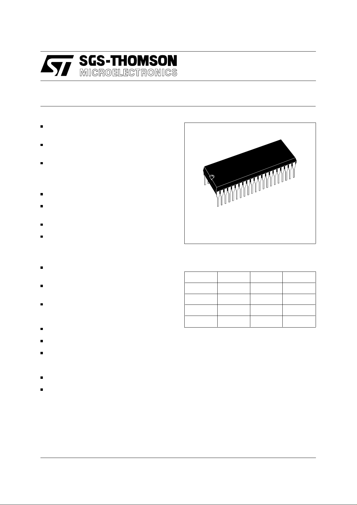
42-lead Shrink DIP package
Interrupt handler and Serial P eripheral Interface
as standard features
31 fully programmable I/O pins
ST9293
48K ROM HCMOS MCUs WITH
FUNCTIONAL DESCRIPTION
PSDIP42
34 character x15 rows software programmable
On Screen Dis play module with colour, italic, underline, flash, transparent and fringe attribute
options
16 bit Timer with 8 bit Presc aler, able to be used
as a Watchdog Timer
16-bit programmable Slice Timer with 8-bit prescaler
4 channel Analog to Digital Converter, with integral sample and hold, fast 5.75µs conversion
time, 6-bit guaranteed resolution
Rich Instruct ion S et and 14 A ddressing modes
Division-by-Zero trap generati on
Versatile Development tools, including assembler,
linker, C-c ompiler, a rchiver, grap hic oriented debugger and hardware emulators
Real Time Operating System
Windowed EPROM parts available for prototyp-
ing and pre-production development phases
(Ordering Information at the end of the Datashe et)
DEVICE SUMMARY
Device ROM RAM PACKAGE
ST9293J7 48K 768 PSDIP42
ST9293J5 32K 640 PSDIP42
ST9293J3 24K 512 PSDIP42
ST9293J1 16K 256 PSDIP42
May 1993
This is Preliminary Data from SGS-THOMSON. Details are subject to change without notice.
1/4
Page 2

ST9293
1.1GENERAL DESCRIPTION
The ST9293 is a ROM member of the ST9 family of
microcontrollers, completely developed and produced by SGS-THOMSON Microelectronics using
a proprietary n-well HCMOS process.
The ROM parts are fully compatible with their
EPROM versions, which may be used for the prototyping and pre-production phases of development, and can be configured as standalone
microcontrollers wit h 48K /32K /24K/ 16 by tes of on chip ROM.
The nucleus of the ST9293 is the advanced Core
which includes the Central Processing Unit (C PU),
the Register File, a 16-bit Timer/Watchdog with 8bit Prescaler, a Serial P eripheral Interface support ing S-bus, I
8-bit I/O ports. The Core has independent memory
and register buses allowing a high degree of pipelining to add to the efficiency of the code execution
speed of the extensive instruction set.Th e powerful
I/O capabilities demanded by microcontroller applications are fulfilled by the ST9293 wit h up to 31/41
I/O lines dedicated to digital Input/Output.
These lines are grouped into up to six I/O Ports and
can be configured on a bit basis under software
2
C-bus and IM-bus Interface, plus two
control to provide timing, status signals, timer inputs and outputs, analog inputs, ext ernal interrupts
and serial or parallel I/O.
Three basic memory spaces are available to support this wide range of configurations: Program
Memory, Data Memory and the Register File,
which includes the control and status registers of
the on-chip peripherals.
The 16-bit Slice Tim er with an 8-bit Prescaler and 6
operating modes allows simple use for waveformgeneration and measurement, PWM functions
and many other system timing functions.
The human interface is provided by the On S creen
Display module, this can produce up to 8 lines of of
up to 34 characters from a ROM defined 128 character set. The 9x13 character can be modified by 4
different pixel sizes, with character rounding, and
formed into words with colour and format attributes.
In addition there is a 4 channel Analog to Digital
Converter with integral s ample and hold, fast 5.5µs
conversion time and 6-bit guaranteed resolution.
Figure 1-1. ST9293 Block Diag ram
16 to 48k x 8
ROM
I/O PORT 0
8
ROM RAM
J7
J5
J3
J1
48K 76 8
32K 64 0
24K 51 2
16K 256
256 to 768
RAM
MEMORY BUS ( Address & Data )
I/O PORT 2
( SPI )
8
256 Bytes
REGISTER F ILE
REGISTER BUS ( Address & Data )
VSYNC
ON SCREEN
DISPLAY
PLL
HSYNC
PLLR
PLLF
I/O PORT 3
AV
DD
16-Bit TIMER / WATCHDOG + SPI
CPU
A/D
CONVERTER
5
( Analog Inputs )
I/O PORT 4
3
SLICE
TIMER
I/O PORT 5
( Control Bus )
( Colour )
7
VR0B1749
2/4
Page 3

1.2 PIN DESCRIPTI ON
ST9293
VSYNC.
Vertical Synch.
Vertical video synchroni-
sation input to OSD. Positive or negative polarity.
HSYNC.
Horizontal Synch.
Horizontal video synchronisation input to OSD. Positive or negative polarity.
PLLF .
PLL Filter input.
Filter input for the OSD for
PLL feed-back.
PLLR .
PLL Resistor connection pin.
For resistor
connection to select the PLL gain adjust.
RESET.
Reset (input, active low).
The ST9 is ini-
tialised by the Reset signal. With the deactivation
RESET, program execut ion begins from the Pro-
of
gram memory location pointed to by the vector
contained in program memory locations 00h and
01h.
OSCIN, OSCOUT.
Oscillator (input and output).
These pins connect a parallel-resonant crystal
(24MHz maximum), or an external source to the
on-chip clock os cillator and buffer. OSCIN is t he input of the oscillator inverter and internal clock g enerator; OSCOUT is the output of the oscillator
inverter.
. Analog VDD of PLL. This pin mus t be tied to
AV
DD
externally to the ST9293.
V
DD
. Main Power Supply Voltage (5V±10%)
V
DD
V
, V
SS
. Digital Circuit Ground, these pins must
SS2
be connected together externally to the ST9293.
P0.0-P0.7, P2.0-P2.7, P3.3-P3.7, P4.5-P4.7,
P5.0-P5.6
CMOS compatible).
I/O Port Lines (Input/Output, TTL or
31 lines grouped into I/O
ports, bit programmable under program control as
general purpose I/O or as Alternate func tions (see
next section).
P3.3 and P3.4 are true 12V open drain outputs
when set in output mode.
1.2.1 I/O Port Alternate Functions.
Each pin of the I/O ports of the ST9293 may assume software programmable Alternative Functions as shown in the Pin Configuration Drawings.
Table 1 shows the Functions alloc ated to e ach I/O
Port pin.
Table 1-1. ST9293 I/O Port Alternate Function Summary
I/O PORT
Port.bit 9293J
P0.0 I/O 12
P0.1 I/O 11
P0.2 I/O 10
P0.3 I/O 9
P0.4 I/O 8
P0.5 I/O 7
P0.6 I/O 6
P0.7 I/O 5
P2.0 INT6 I External Interrupt 6 39
P2.1 INT7 I External Interrupt 7 40
P2.2 INT0 I External Interrupt 0 41
Name Function Alternate Function
Pin
Assignment
3/4
Page 4

ST9293
PIN DESCRIPTI ON (Continued)
Table 1-2. ST9293 I/O Port Alternate Function Summary
I/O PORT
Name Function Alternate Function
Pin
Assignment
Port.bit 9293J
P2.3 INT3 I External Interrupt 3 42
P2.4 WDOUT O T/WD Output 1
P2.4 EXTRG I External A/D Trigger 1
P2.5 SDO O MSPI Serial Data Output 2
P2.6 INT2 I External Interrupt 2 3
P2.6 SCK O SPI Serial Clock 3
P2.7 SDO O SPI Serial Data Output 4
P2.7 SDI I SPI Serial Data Input 4
P3.3 O (12V Open Drain Output) 34
P3.3 SLOUT O Slice Timer Output 34
P3.4 O (12V Open Drain Output) 35
P3.4 SLIN I Slice Timer Input 35
P3.5 INT4 I Schmitt Triggered Input Only 36
P3.6 WDIN I T/WD Input 37
P3.6 AIN4 I A/D Analog Input 4 37
P3.7 NMI I Non-Maskable Interru pt 38
P4.5 AIN5 I A/D Analog Input 5 27
P4.6 AIN6 I A/D Analog Input 6 28
P4.7 AIN7 I A/D Analog Input 7 29
P5.0 I/O 14
P5.1
I/O 15
P5.2 I/O 16
P5.3 FB O Fast Blanking OSD output 17
P5.4 B O Blue Video Colour OSD output 18
P5.5 G O Green Video Colour OSD output 19
P5.6 R O Red Video Colour OSD output 20
Information furnished is believed to be accurate and reliable. However, SGS-THOMSON Microelectronics assumes no responsability for the
consequences of use of such information nor for any infringement of patents or other rights of third parties which may result from its use. No
license is granted by implication or otherwise under any patent or patent rights of SGS-THOMSON Microelectronics. Specifications mentioned
in this publicat ion are subject t o change without not ice. This publication su perse des an d replaces all information previously supplied.
SGS-THOMSON Microelectronics products are not au thor ized for use as critical components in life support devices or systems without the
express written approval of SGS-THOMSON Microelectronics.
© 1995 SGS-THOMSON Microelectronics - All rights reserved.
2
Purchase of I
C Components by SGS-THOMSON Microelectronics conveys a license under the Philips I2C Patent.
Rights to use these components in an I2C system is granted provided that the system conforms to the I2C Standard
Specification as defined by Philips.
SGS-THOMSON Microelectronics Group of Companies
Australia - Brazil - France - Ger many - Hong Kong - Italy - Japan - Korea - Malaysia - Malta - Morocco
The Netherlands - Singapore - Spain - Sweden - Switzerland - Tai wan - Thailand - Uni ted Kingdom - U.S.A.
4/4
 Loading...