

Datasheet ST9291J6, ST9291J7, ST9291J5, ST9291J4, ST9291J3 Datasheet (SGS Thomson Microelectronics)
...Page 1
ST9291
July 1995
16-48K ROM HCMOS MCU WITH
ON SCREEN DISP L A Y AND VOL TA GE TUNINGOU TP UT
(Ordering Information at the end of the Datasheet)
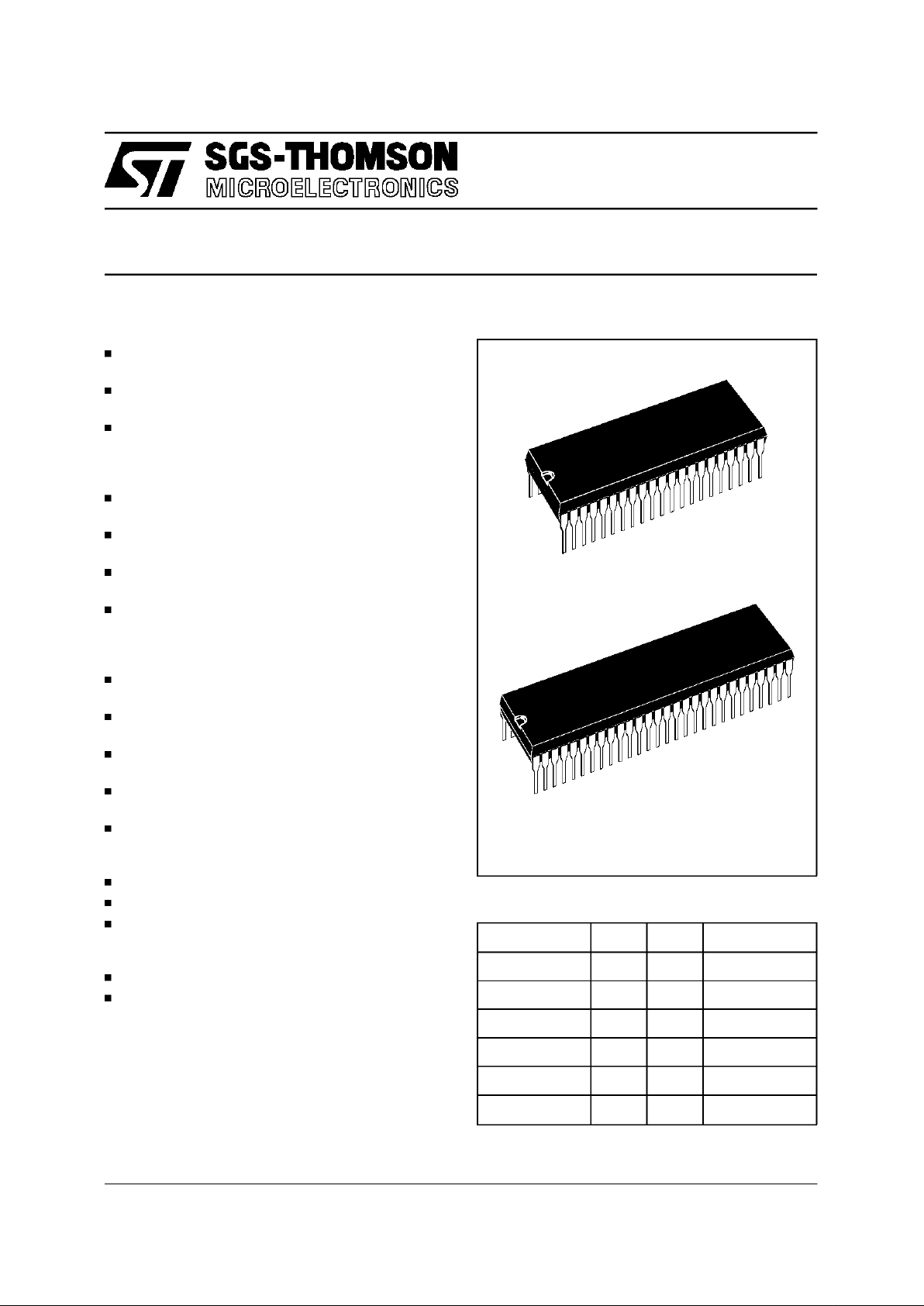
PSDIP42
PSDIP56
Device ROM RAM PACKAGE
ST9291J2/N2 16K 384 PSDIP42/56
ST9291J3/N3 16K 640 PSDIP42/56
ST9291J4/N4 24K 384 PSDIP42/56
ST9291J5/N5 24K 640 PSDIP42/56
ST9291J6/N6 32K 640 PSDIP42/56
ST9291J7/N7 48K 640 PSDIP42/56
DEVICE SUMMARY
Registeroriented8/16 bit COREwith
RUN,WFI andHALT modes
Minimuminstructioncycle time: 500ns
(12MHzinternal)
16 to 48K bytes of ROM,
384/640bytes of RAM,
224generalpurposeregistersavailableasRAM,
accumulatorsor index registers(RegisterFile)
42-leadShrink DIP packageor
56-lead ShrinkDIP package
Interrupthandler and Serial Peripheral Interface
as standardfeatures
31 (42 pin package) / 42 (56 pin package) fully
programmableI/Opins
34 character x15 rows software programmable
On ScreenDisplaymodulewith colour, italic,underline, flash, transparent and fringe attribute
options
14-bit Voltage Synthesis for tuning reference
voltage.
8 8-bit PWM D/A outputswithrepetitionfrequency
2 to 32kHz and12VOpenDrain Capability
16 bit Timer with 8 bitPrescaler, able to beused
as a WatchdogTimer
16-bitprogrammableSlice Timer with 8-bit prescaler
3 channelAnalog to DigitalConverter, withintegral sample and hold, fast 5.75µs conversion
time,6-bit guaranteedresolution
RichInstruction Set and 14 Addressingmodes
Division-by-Zero trap generation
VersatileDevelopmenttools,includingassembler,
linker, C-compiler, archiver,graphic oriented debuggerandhardware emulators
Real TimeOperating System
Windowed EPROM parts available for prototyp-
ing andpre-productiondevelopmentphases
FUNCTIONAL DESCRIPTION
1/20
Page 2
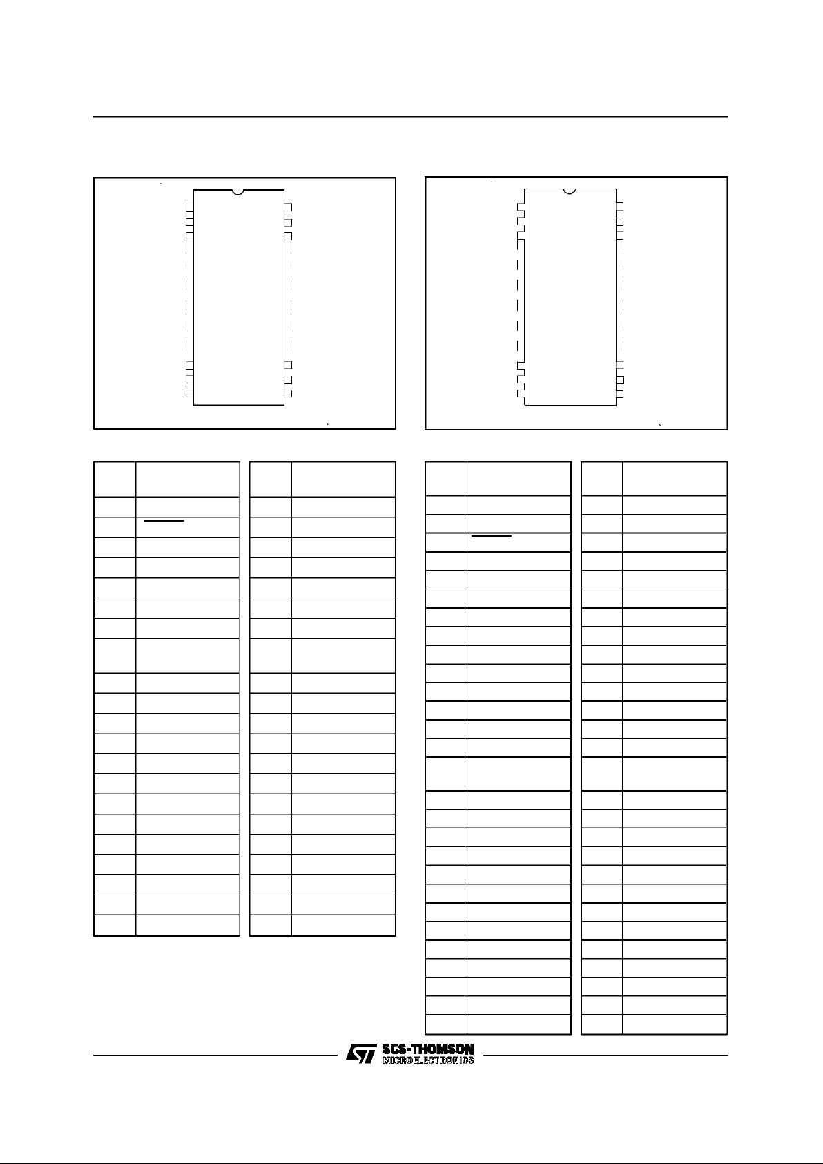
3
19
20
24
23
2221
VR01740B
40
2
1
42
41
Figure 1. 42 Pin Shrink DIP Pinout
Pin
Pin
name
1 P2.0/INT7
2 RESET
3 P0.7
4 P0.6
5 P0.5
6 P0.4
7 P0.3
8 P0.2
9 P0.1
10 P0.0
11 P3.7
12 P3.6
13 P3.5
14 P3.4
15 P3.3/B
16 P3.2/G
17 P3.1/R
18 P3.0/FB
19 P5.1/SDIO
20 P5.0/SCK/INT2
21 V
DD
Pin
Pin
name
42 P2.1/INT5/AIN1
41 P2.2/INT0/AIN2
40 P2.3/INT6/VSO1
39 P2.4/NMI
38 P2.5/AIN3/VSO2
37 OSCIN
36 OSCOUT
35 P4.7/PWM7/
EXTRG (AD)
34 P4.6/PWM6
33 P4.5/PWM5
32 P4.4/PWM4
31 P4.3/PWM3
30 P4.2/PWM2
29 P4.1/PWM1
28 P4.0/PWM0
27 VSYNC
26 HSYNC
25 AV
DD
24 PLLR
23 PLLF
22 V
SS
ST9291JPin Description
Pin
Pin
name
1 P2.1/INT5/AIN1
2 P2.0/INT7
3 RESET
4P0.7
5P0.6
6P0.5
7N.C
.(1)
8P0.4
9P0.3
10 P0.2
11 P0.1
12 P0.0
13 N.C.
(1)
14 V
DD
(2)
15
N.C.
(1)
16 P3.7
17 P3.6
18 P3.5
19 P3.4
20 P3.3/B
21 P3.2/G
22 P3.1/R
23 P3.0/FB
24 P5.3
25 P5.2
26 P5.1/SDIO
27 P5.0/SCK/INT2
28 V
DD
(2)
Pin
Pin
name
56 P2.2/INT0/AIN2
55 P2.3/INT6/VSO1
54 P2.4/NMI
53 P2.5/AIN3/VSO2
52 P1.0
51 P1.1
50 P1.2
49 P1.3
48 P1.4
47 P1.5
46 P1.6
45 P1.7
44 OSCIN
43 OSCOUT
42
P4.7/PWM7/
EXTRG (AD)
41 P4.6/PWM6
40 P4.5/PWM5
39 P4.4/PWM4
38 P4.3/PWM3
37 P4.2/PWM2
36 P4.1/PWM1
35 P4.0/PWM0
34 VSYNC
33 HSYNC
32 AV
DD
31 PLLR
30 PLLF
29 V
SS
ST9291NPin Description
3
26
27
31
30
2928
VR01740A
54
2
1
56
55
Figure2. 56 PinShrink DIP Pinout
Notes (N Package only) :
1. N.C. means “not connected”
2. Pins 14 and 28 (VDD) areinternally connected
ST9291
2/20
Page 3

GENERALDESCRIPTION
The ST9291isa ROMmemberof the ST9familyof
microcontrollers, completely developed and produced by SGS-THOMSON Microelectronicsusing
a proprietaryn-well HCMOS process.
The ROM parts are fully compatible with their
EPROMand OTP (One-TimeProgrammable)versions, which may be used for the prototypingand
pre-productionphasesof development.
The nucleus of the ST9291 is the advancedST9
Core which includes the Central Processing Unit
(CPU), the Register File, a 16-bit Timer/Watchdog
with 8-bit Prescaler, a Serial Peripheral Interface
supporting S-bus, I
2
C-bus and IM-bus Interface,
plus two 8-bitI/O ports. TheCore hasindependent
memory andregisterbuses allowinga high degree
of pipelining to add to the efficiency of the code
executionspeed of the extensive instructionset.
The powerful I/O capabilitiesdemandedby microcontroller applications are fulfilled by the ST9291
with up to 32/42 I/O lines dedicated to digital Input/Output. These lines are groupedinto up to six
I/O Ports and can be configuredon a bit basis under software control to provide timing, status sig-
nals, timer inputs and outputs, analog inputs, external interrupts, OSD (On Screen Display) output
and serialor parallelI/O.
Three basic memoryspaces are available to support this wide range of configurations: Program
Memory, Data Memory and the Register File,
which includes the control and status registers of
the on-chipperipherals.
The humaninterface isprovided by the On Screen
Displaymodule, this can produce up to 15 lines of
up to 34 charactersfrom a ROM defined 128 character set.The 9x13 character canbe modified by4
different pixel sizes, with character rounding, and
formed into words with colour and format attributes.
A 14-bit VS (Voltage Synthesis) output using the
PWM (Pulse Width Modulation)/BRM (Bit Rate
Modulation)is present to generatetuning voltages
for low-mid range TV set applications. The tuning
voltage is output on one of two separate output
pins.
A 16-bit Slice Timer with an 8-bit Prescaleris also
present.
CPU
16-Bit TIMER/WATCHDOG+SPI
SLICE
TIMER
VOLTAGE
SYNTHESIS
I/O PORT 0
8
I/O PORT
3
7
On Screen
Display
PLL
HSYNC
PLLR
PLLF
AV
DD
VSYNC
I/O PORT 4
P.W.M.
Outputs
8
P.W.M.
D/A
Converter
I/O PORT 2
( Analog Inputs )
6
A/D
Converter
I/O PORT 5
( SPI )
2
MEMORY BUS( Address& Data )
REGISTERBUS( Address& Data )
Note : 42 SDIP shown
VR01995E
16 k / 48 k Bytes
ROM or EPROM
(1)
384 / 640 Bytes
RAM
256 Bytes
REGISTER FILE
Figure 3. ST9291 Block Diagram
Note 1. EPROM version only
ST9291
3/20
Page 4

The control of TV or Satellitereceiver setting can
be done by up to eight 8-bit PWM outputs, with a
frequency maximum of 23,437Hz at 8-bit resolution (INTCLK = 12MHz). Low resolutions with
higher frequencyoperationcan be programmed.
Inadditionthereis a3 channelAnalogtoDigitalConverterwithintegralsampleandhold,fast5.75µscon-
versiontimeand6-bitguaranteedresolution.
PIN DESCRIPTION
VSYNC.
VerticalSync.
Verticalvideosynchronisa-
tion inputto OSD. Positiveor negativepolarity.
HSYNC.
Horizontal Sync.
Horizontal video synchronisationinput to OSD. Positiveor negativepolarity.
PLLF.
PLL Filterinput.
Filterinput for the OSD for
PLL feed-back.
PLLR.
PLL Resistor connection pin.
For resistor
connectionto select the PLL gain adjust.
RESET.
Reset(input,active low).
TheST9is initialisedbytheResetsignal.WiththedeactivationofRESET, program execution begins from the Program
memory location pointedto bythe vectorcontained
in programmemorylocations00h and01h.
OSCIN, OSCOUT.
Oscillator (input and output).
These pins connect a parallel-resonant crystal
GENERALDESCRIPTION (Continued)
(24MHz maximum), or an external source to the
on-chipclockoscillatorandbuffer.OSCINis theinput ofthe oscillatorinverter andinternalclock generator; OSCOUT is the output of the oscillator
inverter.
AV
DD
. AnalogVDDof PLL. This pin must betied to
V
DD
externallyto theST9291.
V
DD
. MainPowerSupply Voltage(5V±10%)
V
SS
. Digital Circuit Ground.
P0.0-P0.7, P2.0-P2.5, P3.0-P3.7, P4.0-P4.7,
P5.0-P5.1(J suffix)
P0.0-P0.7, P1.0-P1.7, P2.0-P2.5, P3.0-P3.7,
P4.0-P4.7,P5.0-P5.3 (N suffix)
I/O Port Lines (In-
put/Output,TTLor CMOScompatible).
32/42lines
grouped into I/O ports, bit programmable under
programcontrolas generalpurposeI/O oras Alternate functions(see next section).
P4.0 - P4.7are high voltage(12V) open drainoutputs. Thevoltage inopen drainoutput modefor all
other I/Obits must not exceed V
DD
.
I/O PortAlternate Functions.
Each pin of the I/O ports of the ST9291 may assume software programmable Alternative Functionsas shownin the Pin ConfigurationDrawings.
Table1 shows the Functionsallocated to each I/O
Port pin.
ST9291
4/20
Page 5
PIN DESCRIPTION(Continued)
I/O PORT
Name Function Alternate Function
Pin Assignment
Port.bit 9291J 9291N
P0.0 I/O 10 12
P0.1 I/O 9 11
P0.2 I/O 8 10
P0.3 I/O 7 9
P0.4 I/O 6 8
P0.5 I/O 5 6
P0.6 I/O 4 5
P0.7 I/O 3 4
P1.0 I/O - 52
P1.1 I/O - 51
P1.2 I/O - 50
P1.3 I/O - 49
P1.4 I/O - 48
P1.5 I/O - 47
P1.6 I/O - 46
P1.7 I/O - 45
P2.0 INT7 I External Interrupt 7 with Schmitt Trigger 1 2
P2.1 INT5 I External Interrupt 5 with Schmitt Trigger 42 1
P2.1 AIN1 I A/D Analog Input 1 42 1
P2.2 INT0 I External Interrupt 0 41 56
P2.2 AIN2 I A/D Analog Input 2 41 56
P2.3 INT6 I External Interrupt 6 40 55
P2.3 VSO1 O Voltage Synthesis Output 1 40 55
P2.4 NMI I Non-Maskable Interrupt 39 54
P2.5 AIN3 I A/D Analog Input 3 38 53
P2.5 VSO2 O Voltage Synthesis Output 2 38 53
P3.0 FB O Fast Blanking OSD output 18 23
P3.1 R O Red Video Colour OSD output 17 22
P3.2 G O Green Video Colour OSD output 16 21
P3.3 B O Blue Video Colour OSD output 15 20
Table 1.ST9291 I/O Port Alternative Function Summary
ST9291
5/20
Page 6
PIN DESCRIPTION(Continued)
I/O PORT
Name Function Alternate Function
Pin Assignment
Port.bit 9291J 9291N
P3.4 I/O 14 19
P3.5 I/O 13 18
P3.6 I/O 12 17
P3.7 I/O - 16
P4.0 PWM0 O PWM Output 0 28 35
P4.1 PWM1 O PWM Output 1 29 36
P4.2 PWM2 O PWM Output 2 30 37
P4.3 PWM3 O PWM Output 3 31 38
P4.4 PWM4 O PWM Output 4 32 39
P4.5 PWM5 O PWM Output 5 33 40
P4.6 PWM6 O PWM Output 6 34 41
P4.7 PWM7 O PWM Output 7 35 42
P4.7 EXTRG I A/D External Trigger 35 42
P5.0 SCK O SPI Serial Clock
(1)
20 27
P5.0 INT2 I External Interrupt 2
(1)
20 27
P5.1 SDIO I/O SPI Serial Data Input/Output
(1)
19 26
P5.2 I/O - 25
P5.3 I/O - 24
Notes.
1. The alternate functions of SCK/INT2 and SDIO may be swapped by using the SWAP Register Function.
2. Schmitt trigger options are available as a mask option for any input pin.
Table 1. ST9291 I/O PortAlternativeFunction Summary(Continued)
ST9291
6/20
Page 7

64K
PROGRAM
MEMORY
REGISTER
FILE
64K
DATA
MEMORY
VA00430
Figure 1-4. Address Spaces
1 CORE DESCRIPTION
1.1 COREARCHITECTURE
1.1.1 INTRODUCTION
The Core or Central ProcessingUnit (CPU)of the
ST9 includesthe 8bit ArithmeticLogicUnit and the
16 bit Program Counter, System and User Stack
Pointers.The microcoded InstructionSet is highly
optimised for both byte (8 bit) and word (16 bit)
data, BCD and Boolean data types, with 14 addressingmodes.
Three independent buses are controlled by the
Core, a 16 bit Memory bus, an 8 bit Register addressing bus and a 6 bit Interrupt/DMA bus connected to the interrupt and DMA controllers in the
on-chipperipheralsandtheCore.Thismultiplebus
architectureallows a high degree of pipelining and
parallel operation, giving the ST9 its efficiency in
both numerical calculations and communication
with theon-chipperipherals.
1.1.2 ADDRESS SPACES
The ST9 has threeseparateaddressspaces:
-
Register File: 240 8-bit registers plus up to 64
pages of 16 bytes each, located in the on-chip
peripherals.
-
Data memory with up to 64K(65536) bytes
-
Programmemory with up to 64K (65536) bytes
The Data and Programmemory spaceswill be addressedin furtherdetailin section1.3.
1.1.2.1 RegisterFile
The RegisterFile consistsof:
-
224 general purpose registers R0 toR223
-
16 systemregisters in the SystemGroup
(R224 to R239).
-
I/O pages depending on the configuration of
the ST9, each containing up to 16 registers,
with paging facilities based on the top group
(R240 to R255).
ST9291
7/20
Page 8

ADDRESS SPACES (Continued)
F
E
D
C
B
A
9
8
7
6
5
4
3
PAGED REGISTERS
SYSTEM REGISTERS
2
1
0
00
15
255
240
239
224
223
VA00432
UP TO
64 PAGES
GENERAL
REGISTERS
PURPOSE
224
Figure 1-5. Register Grouping
PAGE 63
PAGE 5
PAGE 0
PAGE POINTER
R255
R240
R224
R0
VA00433
Figure1-6. Page Pointer Configuration
REGISTER FILE
SYSTEM REGISTERS
GROUP D
GROUP B
GROUP C
(1100) (0011)
R192
R207
255
240
239
224
223
F
E
D
C
B
A
9
8
7
6
5
4
3
2
1
0
15
VR000118
00
R195
R195
(R0C3h)
PAGE REGISTERS
Figure 1-7. Addressingthe RegisterFile
ST9291
8/20
Page 9

1.1.2.2 Addressing Registers
All registersin theRegister File and pages can be
specified by using a decimal, hex or binary address, e.g. R231, RE7h or R11100111b is the
same register.
The registers can be referredto by their hexadecimal group address,so that registers R0-R15 form
group 0, R160-R175form group A and so on.
Working Register Addresses
The 8-bit register address is formedby 2 nibbles,
for example, for register R195 or RC3h or
R11000011, 1100 specifies the 13th group (i.e.
group C)and 0011 specifiesthe 3rd registerin that
group.
Working registers are addressedby supplyingthe
leastsignificantnibble intheinstructionandadding
it to the most significant nibble foundin the Register Pointer(R233). Workingregister addressing is
shown in Figure 1-7.
SystemRegisters
The 16 system registers at addresses R224 to
R239 form GroupE.
The systemregistersare addressableusingany of
the 4register addressingmodes and the most significant nibblewill, in all cases, be 14 (0Eh).
Paged Registers
Thereare a maximum of 64pageseach containing
16 registers. Theseare addressedusingthe register addressingmodeswith the additionof thePage
Pointer register, R234. This register selects the
page to be addressed in group F and once set,
does not need to be changedif two or more registers on the same page are to be addressed in succession.
Therefore ifthe PagePointer,R234, isset to 5, the
instructions
spp 5
ld R242, r4
will load the contentsof workingregister r4 intothe
third register(R242) of page 5.
These pagedregistershold dataand controlregisters relatedtothe on-chipperipherals, andthusthe
configurationdependsupon the peripheralorganisation of each ST9 familymember. i.e. pagesonly
exist if the peripheralexists.
Availablepages are shownin Table1-3.
1.1.2.3 Input/Output Ports
The Input/Output ports are located in two areas.
The port registers for Ports 0-5 are located at the
bottom of the System register group in locations
R224 to R229.
Each Port has three associated Control registers,
which determine the individual pin modes (I/O,
Open-Drain etc). These registers are located in
pages 2and 3.
ADDRESS SPACES (Continued)
Hex.
Address
Decimal
Address
Function
Register File
Group
F0-FF 240-255
Paged
Registers
Group F
E0-EF 224-239
System
Registers
Group E
D0-DF 208-223
General
Purpose
Registers
Group D
C0-CF 192-207 Group C
B0-BF 176-191 Group B
A0-AF 160-175 Group A
90-9F 144-159 Group 9
80-8F 128-143 Group 8
70-7F 112-127 Group 7
60-6F 96-111 Group 6
50-5F 80-95 Group 5
40-4F 64-79 Group 4
30-3F 48-63 Group 3
20-2F 32-47 Group 2
10-1F 16-31 Group 1
00-0F 00-15 Group 0
Table 1-2. Register File Organization
ST9291
9/20
Page 10

Applicablefor ST9291
DEC
HEX 00
00
02
02
03
03
0B
11
28
40
29
41
2A
42
3B
59
3E
62
R255 RFF SWAP RESER
VSO
RFF
R254 RFE
SPI
RESER RFE
R253 RFD PORT 3 RESER RFD
R252 RFC WCR RFC
R251 RFB RESER RESER RFB
R250 RFA T/WD RESER RFA
R249 RF9 PORT 2 OSD OSD RESER RF9
R248 RF8 CHAR CHAR OSD RF8
R247 RF7 RESER 1 to 16 17 to 32 PWM RF7
R246 RF6 RF6
R245 RF5 EXT INT PORT1 PORT 5 RF5
R244 RF4 RF4
R243 RF3 RESER RESER OSD RF3
R242 RF2 SLICE CHAR RF2
R241 RF1
RESER
PORT 0 PORT 4 TIMER 33 to36 A/D RF1
R240 RF0 CONV RF0
Table 1-3. Group F PeripheralOrganization
ADDRESS SPACES (Continued)
ST9291
10/20
Page 11

R239 (EFh) SYS. STACK POINTER LOW
R238 (EEh) SYS. STACK POINTER HIGH
R237 (EDh) USER STACKPOINTER LOW
R236 (ECh) USER STACK POINTER HIGH
R235 (EBh) MODE REGISTER
R234 (EAh) PAGE POINTER
R233 (E9h) REGISTER POINTER 1
R232 (E8h) REGISTER POINTER 0
R231 (E7h) FLAGS
R230 (E6h) CENTRAL INT. CNTL REG
R229 (E5h) PORT5
R228 (E4h) PORT4
R227 (E3h) PORT3
R226 (E2h) PORT2
R225 (E1h) PORT1
R224 (E0h) PORT0
Figure 1-8. System Register
1.1.3 SYSTEMREGISTERS
Following isthe description ofSystem Registers.
For PORT0 to PORT5 Registers, please refer to
I/O Port Chapter.
1.1.3.1 CentralInterrupt Control Register
This RegisterCICRis locatedin the systemRegister Group at theaddress R230 (E6h). Please refer
to “INTERRUPT” and “DMA” chapters in order to
get the background of the ST9 interrupt philosophy.
CICR R230 (E6h) System Read/Write
CentralInterrupt Control Register
ResetValue : 10000111
b7 = GCEN:
GlobalCounter Enable
. This bit is the
GlobalCounter Enableof theMultifunctionTimers.
The GCEN bit is ANDedwith the CE (Counter Enable)bitof theTimer Control Register(explained in
the Timer chapter) in order to enable the Timers
when both bits are set. This bit is set after the Reset cycle.
b6 = TLIP:
Top Level Interrupt Pending
. Thisbit is
automatically set when a Top Level Interrupt Request is recognized. This bit can also be set by
Softwarein orderto simulatea Top Level Interrupt
Request.
b5 = TLI:
Top Level Interrruptbit
. When this bit is
set, a TopLevel interrupt requestisacknowledged
depending on the IEN bit and the TLNM bit (in
NestedInterruptControl Register).If theTLM bitis
reset the top level interruptacknowledgementdepends on the TLNM alone.
b4 = IEN:
EnableInterrupt
. Thisbit, (whenset), allows interrupts to be accepted. When reset no interruptsother than theNMI can be acknowledged.
It is clearedby interruptacknowledgementforconcurrent mode and set by interruptreturn (iret). It
can be managed by hardware and software (ei
and di instruction).
b3 = IAM:
InterruptArbitration Mode
. This bit covers the selectionof the two arbitration modes, the
ConcurrentMode being indicated by the value “0”
and the FullyAutomatic Nested Modeby the value
“1”. Thisbit isunder software control.
b2-b0=CPL2-CPL0:
CurrentPriorityLevel
. These
three bits record the priority level of the interrupt
presently under service (i.e. the Current Priority
Level, CPL). For these priority levels 000 is the
highest priority and 111 is the lowest priority. The
CPL bits can be set by hardware or softwareand
givethe referenceby whichfollowinginterruptsare
either left pending or able to interrupt the current
interrupt.Whenthe presentinterruptisreplaced by
one ofa greaterpriority,the currentpriorityvalueis
automaticallystoreduntil required.
ST9291
11/20
Page 12

1.1.3.2 Flag Register
The Flag Register contains 8 flags indicating the
statusoftheST9.Duringaninterrupttheflagregister
is automaticallystoredin thesystemstack area and
recalledat theend of theinterruptservice routine so
that the ST9 is returnedto the original status. This
occursfor all interruptsand, when operatingin the
nestedmode,up tosevenversionsof the flagregistermay bestored.
FLAGR R231 (E7h) System Read/Write
Flag Register
Reset value: undefined
b7 =C:
Carry Flag
. The carry flag C is affectedby
the followinginstructions:
Addition(add, addw, adc, adcw),
Subtraction(sub, subw, sbc, sbcw),
Compare(cp, cpw),
Shift Right Arithmetic(sra, sraw),
Rotate (rrc, rrcw, rlc, rlcw, ror, rol),
DecimalAdjust (da),
Multiplyand Divide (mul, div, divws).
When set, it generally indicates a carry out of the
most significant bit position of the register being
used asan accumulator(bit7 forbyte andbit15 for
word operations).
ThecarryflagcanbesetbytheSetCarryFlag(scf)
instruction,clearedbytheResetCarryFlag(rcf)in-
struction,and complemented(changedto “0” if “1”,
andviceversa) bytheComplementCarryFlag(ccf)
instruction.
b6 =Z:
Zero Flag
. The Zero flag is affectedby the
followinginstructions:
Addition(add, addw, adc, adcw),
Subtraction(sub, subw, sbc, sbcw),
Compare(cp, cpw),
Shift Right Arithmetic(sra, sraw),
Rotate (rrc, rrcw, rlc, rlcw, ror, rol),
DecimalAdjust (da),
Multiplyand Divide (mul, div, divws),
Logical (and, andw, or, orw, xor, xorw,
cpl),
Increment and Decrement (inc, incw, dec,
decw),
Test (tm, tmw, tcm, tcmw, btset).
In most cases,the Zero flag is setwhenthe register
beingused as an accumulator register is zero, following oneof theabov eoperations .
b5 = S:
SignFlag
. TheSign flag is affected by the
sameinstructions asthe Zeroflag.
The Sign flag is set when bit 7 (for byte operation)
or bit15(for wordoperation)of theregisterusedas
an accumulatoris one.
b4 = V:
Overflow Flag
. The Overflow flag is affected by the same instructions as the Zero and
Sign flags.
Whenset, theOverflow flagindicates that a two’scomplementnumber,in a resultregister,isin error,
since it has exceeded the largest (or is less than
the smallest), number that can be represented in
twos-complementnotation.
b3 =DA:
DecimalAdjust Flag
. TheDecimal Adjust
flagis usedfor BCDarithmetic.Sincethealgorithm
for correctingBCD operations is different for addition and subtraction, this flag is used to specify
whichtype of instructionwas executedlast, so that
the subsequentDecimalAdjust (da) operationcan
performits functioncorrectly.
The Decimal Adjust flag cannot normally be used
as a test condition by the programmer.
b2 = H:
Half Carry Flag
. The Half Carry flag indicates a carry out of (or a borrow into) bit 3, as the
resultof addingorsubtractingtwo8-bit bytes,each
representingtwo BCD digits.The Half Carry flagis
used bythe DecimalAdjust (da) instructionto convert the binary result of a previousadditionor subtraction intothe correct BCD result.
Like the Decimal Adjust flag, this flag is not normallyaccessed by the user.
b1 =UF:
UserFlag
. Bit1 in the flagregister (UF) is
available to the user, but it must be set or cleared
by an instruction.
b0 = DP:
Data/Program Memory Flag
. This bit in
the flag register indicates which memory area is
addressed. Its value is affected by the Set Data
Memory(sdm) andSet Program Memory (spm) instructions.
If the bit is set, theST9 addressesthe Data Memory Area; when the bit is cleared, the ST9 addresses the Program Memory Area. By reading
this bit, the user can verify in which memory area
the processor is working. The user writes this bit
with the sdm or spm instructions.
SYSTEM REGISTERS(Continued)
ST9291
12/20
Page 13

1.1.3.3 Register Pointing Techniques
Two registers, R232 and R233, within the system
register group, are available for register pointing.
R232 and R233 may be used togetheras a single
pointer for a 16 register working space or separately for two 8 register spaces, in which case
R232 becomesRegisterPointer0 (RP0)andR233
becomesRegister Pointer1 (RP1).
The instructions srp, srp0 and srp1 (the Set
RegisterPointer instructions)automaticallyinform
the ST9whetherthe RegisterFile isto operatewith
a single16-registergroupor two 8-registergroups.
The srp0 andsrp1 instructionsautomaticallyset
the twin 8-register group mode while the srp instruction sets the single 16-register group mode.
There is no limitation on the order or positions of
these chosenregister groupsother than they must
be on 8or 16 registerboundaries.
Theaddressingof working registersinvolves use of
the RegisterPointervalueplusanoffsetvaluegiven
by thenumberofthe addressedworking register.
When addressing a register, the most significant
nibble (bits 4-7) gives the group address and the
least significantnibble (bits 0-3) gives the register
within that group.
REGISTERPOINTER0
RP0 R232 (E8h) System Read/Write
RegisterPointer 0
Reset Value: undefined
b7-b3=RG7-RG3:
RegisterGroupnumber
. These
bits containthe number (from0 to31) of the group
of working registers indicated in the instructions
srp0 or srp. When using a 16-register group, a
numberbetween 0 and 31 must be used in the srp
instructionindicatingoneof thetwo adjacent8-register group of working registers used. RG7 is the
MSB.
b2 = RPS:
Register PointerSelector
. This bit is set
by theinstructionssrp0 and srp1 to indicatethat a
double register pointing mode is used. Otherwise,
theinstructionsrp resetstheRPSbittozeroto indicate that a single registerpointing modeis used.
b1,b0= D1,D0:Thesebits arefixed byhardwareto
zero and arenot affectedby any writinginstruction
trying to modify theirvalue.
REGISTERPOINTER1
RP1 R233 (E9h) System Read/Write
RegisterPointer 1
ResetValue : undefined
This register is used only with double register
pointing mode; otherwise, using single register
pointingmode, theRP1Rregisterhasto beconsidered as reserved and not usableas a generalpurpose register.
b7-b3=RG7-RG3:
RegisterGroupnumber
. These
bits containthe number (from 0 to 31) of the group
of 8 working registers indicated in the instructions
srp1. Bit7 is the MSB.
b2 = RPS:
Register Pointer Selector
. This bit is
automatically set by the instructions srp0 and
srp1 to indicate that a double register pointing
mode is used. Otherwise the instruction srp reset
the RPSbit to zero to indicatethat a singleregister
pointingmode is used.
b1,b0 = D1,D0: These bits are hardware fixed to
zero andare notaffectedby anywriting instruction
tryingto modifytheir value.
Note. If working in twin 8-registergroup mode but
only using srp0 (i.e. only using one 8-register
group) the unused register (R233) is to be considered as reserved and not usableas a generalpurpose register.
The group of registers immediatelybelow the system registers (i.e. group D, R208-R223) can only
be accessedvia the RegisterPointers. To address
group D then, it is necessary to set the Register
Pointer to group D and then use the addressing
procedure for working registers. The programmer
is requiredtorememberthatthe groupD shouldbe
used as a stackingarea. Thispoint is also covered
in the Stack Pointersparagraph.
SYSTEM REGISTERS(Continued)
ST9291
13/20
Page 14

EXAMPLES
Using the Single 16 Register Group
When the systemis operating in the single 16-register group mode, the registers are referred to as
r0-r15. In this mode, the offset value(i.e. the number of the workingregister referred to) is supplied
in theaddress (preceded by a smallr, e.g.r5) and
is addedtothe RegisterPointer0 valueto give the
absoluteaddress.
For example, if the Register Pointer contains the
value 70h,then working register r7would havethe
absoluteaddress, R77h.
In this mode, the single16-registers group will always start from the lowest even number equal or
lower to the number givenin theinstruction.
Example:srp #3 isequivalent to srp #2.
Usingthe Twin 8-Register Group
Whenworking in the twin workinggroup mode,the
registerspointedbyRegisterPointer0(RP0R),are
referred as r0-r7 and those pointed by Register
Pointer1 (RP1R),are referred to asr8-r15, regardless of their absolute addresses. In this mode,
when operating with the first 8 working registers
(i.e. r0 -r7) theworking registernumber acts as an
offset which is added to the value in Register
Pointer0.
So if RegisterPointer0 containsthevalue 96, then
working register 0 has the absolute address 96,
working register 5 has the absolute address 101,
and so on. The second group of workingregisters,
r8-r15,hasthe offsetvalues 0to 7respectively(i.e.
r8 hasthe offset value 0, r9 has the offset value1,
and so on), this offset value being added to the
value in Register Pointer1.
For example, given that the value in Register
Pointer 1 is 32, then working register 12 supplies
an offset value of 4 (given by 12 minus 8) to the
value in Register Pointer 1 to give an absolute addressof 36.
SYSTEM REGISTERS(Continued)
GROUP F
VA00097
WORKING
REGISTER POINTER 0
255
240
239
r15
r0
GROUP E
GROUP 4
0
224
REGISTER
Figure 1-9. Single 16Register pointing Mode
GROUP F
VA00098
REGISTER POINTER 1
REGISTER POINTER 0
255
240
239
224
r7
r0
r15
r8
GROUP E
GROUP 8
GROUP 3
0
WORKING REGISTER
WORKING REGISTER
Figure1-10. Double Register pointingMode
ST9291
14/20
Page 15

1.1.3.4 Page Configuration
The pages are availableto be used for the storage
of control information (such as interrupt vector
pointers) relevant to particular peripherals. There
are up to 64 pages (eachwith 16registers) based
on registers R240-R255. These paged registers
are addressable via the page pointer register
(PPR),which issystem registerR234.
To addressa pagedregister the pagepointerregister (R234) must be loaded with the relevant page
numberusing thespp instruction(SetPagePointer)
and subsequently any address from the top (F)
group(R240-R255)will be referredtothatpage.
For example if register 23 contains the value 44,
the following sequence loads the third register
R242 on page 5 with the value 44.
spp 5
ld R242, R23
PPR R234 (EAh) System Read/Write
Page Pointer Register
Reset value: undefined
70
PP7 PP6 PP5 PP4 PP3 PP2 D1 D0
b7-b2 = PP7-PP2:
Page Pointer
. These bits contain the number(between0 to63) of thepage chosen by theinstructionssp (SetPage Pointer).PP7
is the MSB of the page address. Once the page
pointer has been set, thereis no need to refresh it
unless a differentpage is required.
b1-b0=D1,D0: Thesebitsarefixedby hardwareto
zero and arenot affectedby any writinginstruction
trying to modify theirvalue.
PAGE 0 containsthe control registersof:
-
the external interrupt
-
the watchdog timer
-
the wait logic states
-
the serial peripheral interface(SPI)
1.1.3.5 Mode Registers
This register MODER is located in the System
RegisterGroup at theaddress235.
Using thisregister it is possible:
-
to select either internal or external System and
User Stack area,
-
to managethe clock frequency
-
to enable the Bus request and Wait signals
when interfacingexternal memory.
MODER R235 (EBh) System Read/Write
ModeRegister
Resetvalue : 11100000
70
SSP USP DIV2 PRS2 PRS1 PRS0 BRQEN HIMP
b7 = SSP:
System Stack Pointer
. This bit selects
internal (inthe RegisterFile) or external(in the external Data Memory) System Stack area, logical
“1” for internal, and logical “0” for external. After
Resetthe value ofthis bit is “1”.
b6 = USP:
User Stack Pointer
. Same as bit 7 for
the UserStack Pointer;
b5 =DIV2:
OSCINClockDividedby2
. Thisbitcontrols the divide by 2 circuit which operates on the
OSCIN Clock. A logical “1” value means that the
OSCINclockisinternallydividedby2, andalogical
“0” value means that no division of the OSCIN
Clockoccurs.
b4-b2 = PRS2-PRS0:
ST9 CPUCLK Prescaler
.
These bits load the prescaling module of the internal clock (INTCLK). The prescaling value selects
the frequency of the ST9 clock, which can be divided by 1 to 8. See Clock chapter for more information.
b1 = BRQEN:
BusRequest Enable
. This bit must
be held to “0”.
b0 =HIMP:
HighImpedanceEnable
. Thisbit must
be held to “0”.
SYSTEM REGISTERS(Continued)
ST9291
15/20
Page 16

SYSTEM REGISTERS(Continued)
1.1.3.6 Stack Pointers
There are two separate, double register stack
pointers available (named System Stack Pointer
and User Stack Pointer), both of which can address registersor memory.
The stackpointerspointto thebottom ofthe stacks
which are filled using the push commands and
emptied using the pop commands. The stack
pointer is automatically pre-decremented when
data is “pushed in” and post-incremented when
data is “poppedout”.
For example, the register address space is selected for a stack and the corresponding stack
pointer registercontains 220. When a byte of data
is “pushed”into thestack, thestackpointerregister
is decremented to 219, then the data byte is
“loaded” into register 219. Conversely, if a stack
pointer register contains 189 and a byte of data is
“popped” out, the byte of data is then extracted
fromthe stack andthenthe stackpointerregisteris
incrementedto 190.
The push and pop commands used to manage
the system stack area are made applicable to the
user stack by adding the suffix U, while to use a
stack instructionfor a worda W is added.
For example push inserts data into the system
stack, butan addedU indicatesthe user stack and
W meansa word, so theinstruction pushuw loads
a wordinto the bottomof theuser stack.
If the User Stack Pointer register contains 223
(workingin register space) theinstruction pushuw
will decrement User Stack Pointer register to 222
and then load a wordinto registerR222 and R221.
Whenbytes (orwords)are “poppedout”the values
in those registers are left unchanged until fresh
data is loaded into those locations. Thus when
data is “popped” out from a stack area, the stack
content remains unchanged.
Note. Stacks must not be locatedin the pages or
the systemregister area.
The System Stack area and The System Stack
Pointer
The System Stack area is used for the storage of
temporarilysuspended systemand/or control registers, i.e. the Flag register and the Program
counter, while interrupts are being serviced. For
subroutine execution only the Program Counter
needs to be saved in theSystem stack area.
Therearetwosituationswhenthisoccurs automatically,one being when an interruptoccurs and the
other when the instructioncall subroutine is used.
Whenthe systemstack area isin theRegister File,
the stackpointer, which points to the bottom of the
stack,onlyneedsone bytefor addressing,inwhich
case the System Stack Pointer Low Register
(R239) is sufficient for addressing purposes.As a
result the System Stack Pointer High Register
(R238) becomes redundant BUT must be considered as reserved (please refer also to “spurious”
memoryaccesssection). Clearlywhenthe stack is
external a full word address is necessary and so
both registersare usedto point, the even register
providing the MSB and the odd register providing
the LSB.
The User Stackarea and User Stack Pointer
TheUser Stackarea is completelyfree fromall interferencefromautomaticoperationsand soit provides a totally user controlled stacking area, that
area being in any part of the memorywhich is of a
RAM nature, or the first 14 groups of the general
Register File i.e. not in the System register or
Pagedgroup.
The User Stack Pointer consists of two registers,
R236 and R237, which are both usedfor addressing an external stack, while, when stacking in the
Register File, the User Stack Pointer High Register, R236,becomesredundantbut mustbe considered as reserved.
ST9291
16/20
Page 17

Stack location
Care is necessarywhenmanaging stacksas there
is no limit to stack sizes apart from the bottom of
any address space in which the stack is placed.
Consequently programmers are advised to use a
stackpointervalue ashigh as possible,particularly
when using the Register File as a stacking area.
This willalso benefit programmers who maylocate
the stacks in group D using, for example the instruction ld R237, #223 which loads the value
SYSTEM REGISTERS(Continued)
STACK POINTER L
STACK
VA00434
R255
R0
STACK POINTER H
REGISTER FILE
Figure 1-11. System and/orUser Stack in
Register Stack Mode
STACK POINTER L
SYSTEM REGISTERS
STACK
DATA MEMORY
VA00435
STACK POINTER H
Figure1-12. System and/or User Stack in
MemoryStack Mode
223 into the User Stack PointerLow Register. The
Programmerwill not need to remember to set the
Register Pointerto 208 to gainaccess to registers
in the D-group, a problem outlined in Register
PointingTechniquesparagraph.
Stacks may be located anywhere in the first 14
groups of the RegisterFile (internal stacks) or the
data memory (external stacks).It is not necessary
to set the data memory using the instructionsdm
as externalstackinstructionsautomaticallyusethe
data memory.
USP R236 (ECh) System Read/Write
User StackPointer High Byte
Reset value: undefined
USP R237 (EDh) System Read/Write
User StackPointer Low Byte
Reset value: undefined
SSP R238 (EEh) System Read/Write
SystemStack PointerHigh Byte
Resetvalue: undefined
SSP R239 (EFh) System Read/Write
SystemStack PointerLow Byte
Resetvalue: undefined
1.2 MEMORY
ST9291
17/20
Page 18

1.2.1 INTRODUCTION
The memory of the ST9291 is functionallydivided
into two areas, theRegister File and Memory. The
Memorymayoptionallybe dividedinto twospaces,
Program Memory for Program code and Data
Memory forData.
The memoryspaces areselected by the execution
of the SDM and SPM instructions (Set Data Memory and SetProgramMemory, respectively).There
is noneed to useeither of these instructionsagain
until the memoryarea requiredis to be changed.
1.2.1.1 Program Space
The Program memory space of the ST9291 consistsof 48Kbytesof on-chipROM(addressedfrom
0 to BFFF) and 640 bytes of on-chip RAM (addressed from FD80h to FFFFh); refer to the memory map tables and drawingon the followingpage
for the memorymappingfor other ROM sizes.The
first 256 memory locations from address 0 to
00FFh (hexadecimal) hold the Reset Vector, the
Top-Level (Pseudo Non-Maskable) interrupt, the
Divide by Zero Trap vector and, optionally, the
interrupt vector table for use with the on-chip
peripherals and the external interrupt sources.
Each vector is contained in two consecutive byte
locations,the high order addressheld inthe lower
(even) byte, the low order address held in the upper (odd) byte, forming the address which is
loaded into the Program Counter when selected
by the interrupt vector provided by the interrupt
source. This should point to the relevant Interrupt
Service routine provided by the User for immediate response to the interrupt.
1.2.1.2 Data Space
The ST9291 addresses the 640 bytes of on-chip
RAM memory from addresses FD80h to FFFFh in
both Program and Data Space. On-chip general
purposeRegistersmaybe usedas additionalRAM
memoryfor minimum chipcount systems.
The Data Space is selected by the execution of
the SDM instruction. All subsequent memory references will access the Data Space. When a
separate Data Space is not required, data may
stored in RAM or ROM memory within the Program Space.
ST9291
18/20
Page 19

MEMORY (Continued)
VR01354I
INTERNAL RAM
MAPPED BOTH INTO PROGRAM AND DATA SPACE
DATA
65535
0
PROGRAM
ROM
RAM
24K
64896
32767
24575
16383
32K
16K
ROM
ROM
49151
48K
Figure 1-13. ST9291 Memory Map
Device Suffix
ROM Size
(Bytes)
ROM Addresses
RAM Size
(Bytes)
RAM Addresses
J2/N2 16K
0 - 16383 dec
384
64896 - 65279 dec
0000 - 3FFF hex FD80 - FEFF hex
J3/N3 16K
0 - 16383 dec
640
64896 - 65535 dec
0000 - 3FFF hex FD80 - FFFF hex
J4/N4 24K
0 - 24575 dec
384
64896 - 65299 dec
0000 - 5FFF hex FD80 - FEFF hex
J5/N5 24K
0 - 24575 dec
640
64896 - 65535 dec
0000 - 5FFF hex FD80 - FFFF hex
J6/N6 32K
0 - 32767 dec
640
64896 - 65535 dec
0000 - 7FFF hex FD80 - FFFF hex
J7/N7 48K
00000 - 49151 dec
640
64896 - 65555 dec
0000 - BFFF hex FD80 -FFFF hex
Table 1-4. ROM and RAM Address Configuration
ST9291
19/20
Page 20

Notes:
Information furnished is believed to be accurateand reliable. However, SGS-THOMSON Microelectronics assumes no responsability for the
consequences of use of such informationnor for any infringement of patents or other rights of third parties which may result from its use. No
licenseis granted by implication or otherwise under any patent or patent rights of SGS-THOMSON Microelectronics. Specifications mentioned
in this publication are subject to changewithout notice. This publication supersedes and replaces all informationpreviously supplied.
SGS-THOMSON Microelectronics products are not authorized for use as critical components in life support devices or systems without the
express written approval of SGS-THOMSON Microelectronics.
1995 SGS-THOMSONMicroelectronics - All rights reserved.
Purchase of I
2
C Components by SGS-THOMSON Microelectronicsconveys a license under the Philips I2C Patent.
Rights touse these components in an I
2
C system is granted provided that the system conforms to the I2C Standard
Specification asdefined byPhilips.
SGS-THOMSON Microelectronics Group ofCompanies
Australia -Brazil - France -Germany - Hong Kong - Italy - Japan - Korea - Malaysia - Malta - Morocco - The Netherlands
Singapore -Spain -Sweden -Switzerland - Taiwan - Thailand- United Kingdom - U.S.A.
ST9291
20/20
 Loading...