

Page 1
ON-SCREEN-DISPLAY AND TELETEXT DATA SLICER
■ Register File based 8/16 bit Core Architecture
with RUN, WFI, SLOW and HALT modes
■ 0°C to +70°C operating temperature range
■ Up to 24 MHz. operation @ 5V±10%
■ Min. instruction cycle time: 165nsat 24 MHz.
■ 32, 48, 56 or 64 Kbytes ROM
■ 256 bytesRAM of Register file (accumulators or
index registers)
■ 256 bytes of on-chip static RAM
■ 2, 6 or 8 Kbytes of TDSRAM (Teletext and
Display Storage RAM)
■ 28 fully programmable I/O pins
■ Serial Peripheral Interface
■ Flexible Clock controller for OSD, Data Slicer
and Core clocks running from a single low
frequency external crystal.
■ Enhanced display controller with 26 rows of
40/80 characters
– Serial and Parallel attributes
– 10x10 dot matrix, 512 ROM characters, defin-
able by user
– 4/3 and 16/9 supported in 50/60Hz and 100/
120 Hz mode
– Rounding, fringe,doublewidth, double height,
scrolling, cursor, full background color, halfintensity color, translucency and half-tone
modes
■ Teletext unit, including Data Slicer, Acquisition
Unit and up to 8 Kbytes RAM for data storage
■ VPS and Wide Screen Signalling slicer (on
some devices)
■ Integrated Sync Extractor and Sync Controller
■ 14-bit Voltage Synthesis for tuning reference
voltage
■ Up to 6 external interrupts plus one Non-
Maskable Interrupt
■ 8 x 8-bit programmable PWM outputs with 5V
open-drain or push-pull capability
■ 16-bit watchdog timer with 8-bit prescaler
■ One 16-bit standard timer with 8-bit prescaler
■ 4-channel A/D converter; 5-bit guaranteed
ST92195B
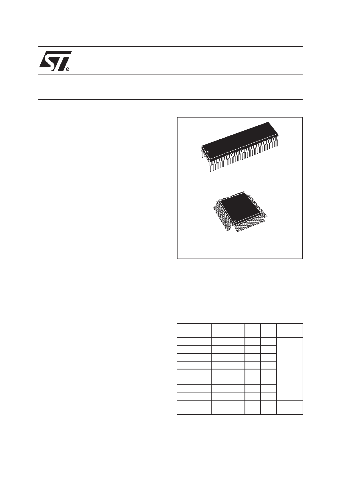
32-64K ROM HCMOS MCU WITH
DATA BRIEFING
PSDIP56
TQFP64
See end of document for ordering information
■ Rich instruction set and 14 addressing modes
■ Versatile development tools, including
Assembler, Linker, C-compiler, Archiver,
Source Level Debugger and hardware
emulators with Real-Time Operating System
available from third parties
■ Pin-compatible EPROM and OTP devices
available
Device Summary
Device
ST92195B1 32K ROM 2K Yes
ST92195B2 32K ROM 6K No
ST92195B3 32K ROM 6K Yes
ST92195B4 48K ROM 6K Yes
ST92195B5 48K ROM 8K Yes
ST92195B6 56K ROM 8K Yes
ST92195B7 64K ROM 8K Yes
ST92T195B7 64K OTP 8K Yes
ST92E195B7 64K EPROM 8K Yes
Program
Memory
TDS
RAM
VPS/
WSS
Package
PSDIP56/
TQFP64
CSDIP56
/CQFP64
Rev. 2.5
January 2000 1/22
1
Page 2

ST92195B - GENERAL DESCRIPTION
1 GENERAL DESCRIPTION
1.1 INTRODUCTION
The ST92195B microcontroller is developedand
manufactured by STMicroelectronics using a proprietary n-well HCMOS process. Its performance
derives from the use of a flexible 256-register programming model for ultra-fast context switching
and real-time event response. The intelligent onchip peripherals offload the ST9 core from I/O and
data management processing tasks allowing critical application tasks to get the maximum use of
core resources.The ST92195B MCUsupports low
power consumption and low voltage operation for
power-efficient and low-cost embedded systems.
1.1.1 ST9+ Core
The advanced Core consists of the Central
Processing Unit (CPU), the Register File and the
Interrupt controller.
The general-purpose registers can be used as accumulators, index registers, or address pointers.
Adjacent registerpairs make up 16-bit registers for
addressing or 16-bit processing. Although the ST9
has an 8-bit ALU, the chip handles 16-bit operations, including arithmetic, loads/stores, and memory/register and memory/memory exchanges.
Two basic addressable spaces are available: the
Memory space and the Register File, which includes the control and status registers of the onchip peripherals.
1.1.2 Power Saving Modes
To optimize performance versus power consumption, a range of operating modes can be dynamically selected.
Run Mode. This is the full speed execution mode
with CPU and peripherals running at themaximum
clock speed delivered by the Phase Locked Loop
(PLL) of the Clock Control Unit (CCU).
Wait For Interrupt Mode. The Wait For Interrupt
(WFI) instruction suspends program execution until an interrupt request is acknowledged. During
WFI, the CPU clock is halted while the peripheral
and interrupt controller keep running at a frequen-
cy programmable via the CCU. In this mode, the
power consumption of the device can be reduced
by more than 95% (Low power WFI).
Halt Mode. When executing the HALT instruction,
and if the Watchdog is not enabled, the CPU and
its peripherals stop operating and the status of the
machine remains frozen (the clock is also
stopped). A reset is necessary to exit from Halt
mode.
1.1.3 I/O Ports
Up to 28 I/O lines are dedicated to digital Input/
Output. Theselines are grouped into up to five I/O
Ports and can be configured on a bit basis under
software control to provide timing, status signals,
timer and output,analog inputs,external interrupts
and serial or parallel I/O.
1.1.4 TV Peripherals
A set of on-chip peripherals form a complete system for TV set and VCR applications:
– Voltage Synthesis
– VPS/WSS Slicer
– Teletext Slicer
– Teletext Display RAM
– OSD
1.1.5 On Screen Display
The human interface is provided by the On Screen
Display module, this can produce up to 26 lines of
up to 80 characters from a ROM defined 512 character set. The character resolution is 10x10 dot.
Four character sizes are supported. Serial attributes allow the user to select foreground and
background colors, charactersizeand fringe background. Parallel attributes can be used to select
additional foreground and background colors and
underline on a character by character basis.
1.1.6 Teletext and Display Storage RAM
The internal Teletext and Display storage RAM
can be usedtostore Teletext pages aswell as Display parameters.
2/22
Page 3

INTRODUCTION (Cont’d)
1.1.7 Teletext, VPS and WSS Data Slicers
The three on-board data slicers using a single external crystal are used to extract the Teletext, VPS
and WSS information from the video signal. Hardware Hamming decoding is provided.
1.1.8 Voltage Synthesis Tuning Control
14-bit Voltage Synthesis using the PWM (Pulse
Width Modulation)/BRM (Bit Rate Modulation)
technique canbeused togenerate tuning voltages
for TV set applications. The tuning voltage is output on one of two separate output pins.
1.1.9 PWM Output
Control of TV settings can be made with up to
eight 8-bitPWMoutputs,with a maximumfrequency of 23,437Hz at 8-bit resolution (INTCLK = 12
MHz). Low resolutions withhigher frequency operation can be programmed.
ST92195B - GENERAL DESCRIPTION
1.1.10 Serial Peripheral Interface (SPI)
The SPI bus is used to communicate with external
devices v ia the SPI, or I C bus communication
standards. The SPI uses a single data line for data
input and output. A se cond l ine is used for a synchronous c lock signal.
1.1.11 Standard Timer (STIM)
The ST92195B has one Standard Timer (STIM0)
that includes a programmable 16-bit down counter
and an associated 8-bit prescaler with Single and
Continuous counting modes.
1.1.12 Analog/Digital Converter (ADC)
In addition there is a 4-channel Analog to Digital
Converter with integral s ample and hold, fast
5.75µs conversion time and6-bit guaranteed resolution.
3/22
Page 4

ST92195B - GENERAL DESCRIPTION
INTRODUCTION (Cont’d)
Figure 1. ST92195B Block Diagram
NMI
INT[7:4]
INT2
INT0
OSCIN
OSCOUT
RESET
RESETO
SDO/SDI
SCK
MCFM
STOUT
VSO[2:1]
Up to 64
Kbytes ROM
256 bytes
RAM
Up to 8
Kbytes
TDSRAM
256 bytes
Register File
Management
ST9+ CORE
WATCHDOG
TIMING AND
CLOCK CTRL
STANDARD
VOLTAGE
SYNTHESIS
TRI
8/16-bit
CPU
MMU
Interrupt
RCCU
16-BIT
TIMER/
SPI
TIMER
MEMORY BUS
REGISTER BUS
I/O
PORT 0
I/O
PORT 2
I/O
PORT 3
I/O
PORT 4
I/O
PORT 5
DATA
SLICER
& ACQUI-
SITION
UNIT
SYNC.
EXTRAC-
TION
VPS/WSS
DATA
SLICER
ADC
SYNC
CONTROL
ON
SCREEN
DISPLAY
PWM
D/A CON-
VERTER
8
6
4
8
2
FREQ.
MULTIP.
P0[7:0]
P2[5:0]
P3[7:4]
P4[7:0]
P5[1:0]
TXCF
CVBS1
WSCR
WSCF
CVBS2
AIN[4:1]
EXTRG
VSYNC
HSYNC/CSYNC
CSO
PXFM
R/G/B/FB
TSLU
HT
PWM[7:0]
4/22
All alternate functions
(Italic characters)
are mapped on Ports 0,2, 3, 4 and 5
Page 5
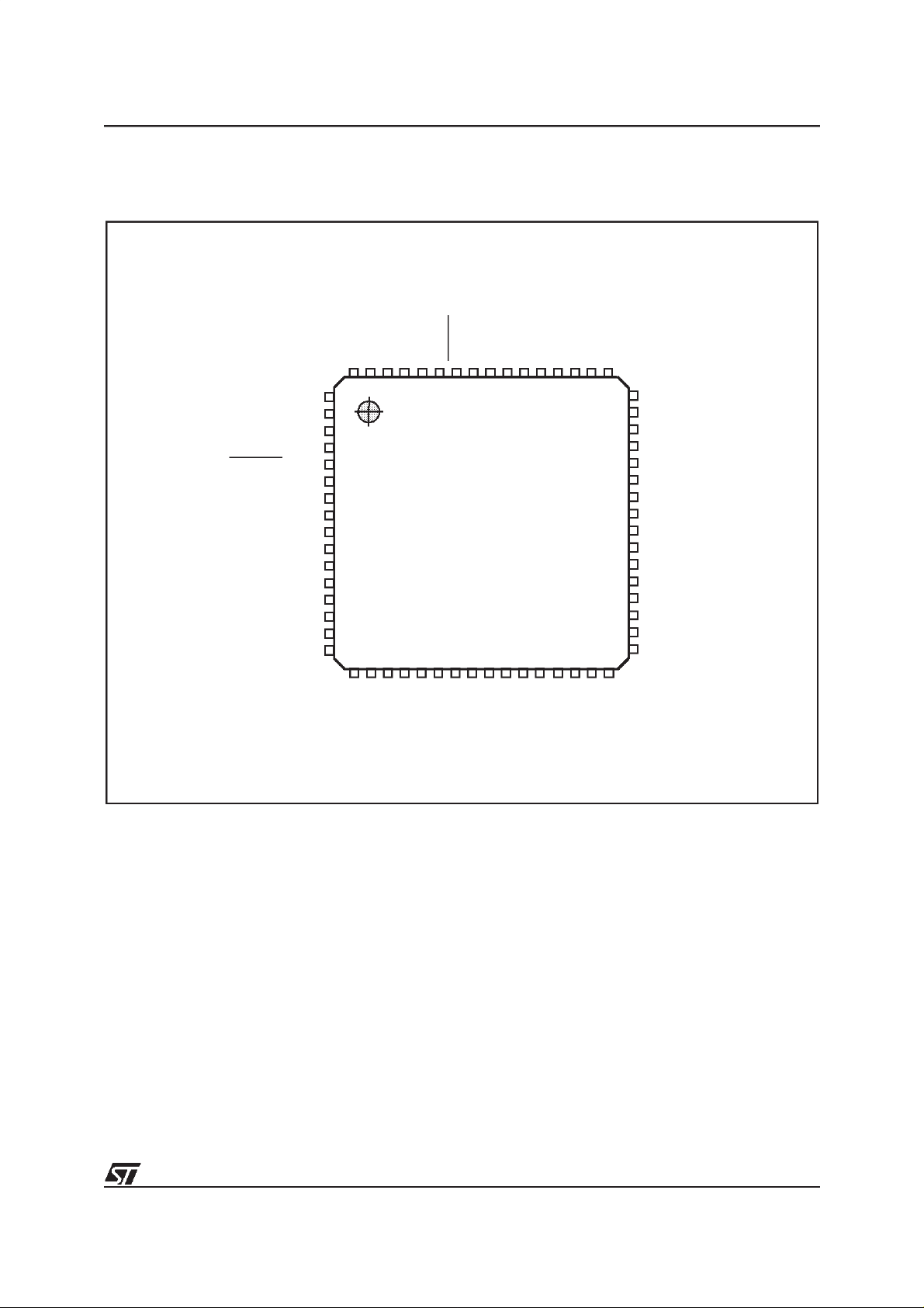
1.2 PIN DESCRIPTION
Figure 2. 64-Pin Package Pin-Out
ST92195B - GENERAL DESCRIPTION
GND
AIN4/P0.2
P0.1
P0.0
CSO/RESET0/P3.7
P3.6
P3.5
P3.4
FB
SDO/SDI/P5.1
INT2/SCK/P5.0
V
DD
JTDO
VDDP0.3
P0.4
P0.5
P0.6
P0.7
RESET
P2.0/INT7
P2.1/INT5/AIN1
P2.2/INT0/AIN2
P2.3/INT6/VS01
P2.4/NMI
P2.5/AIN3/INT4/VS02
64
1
B
G
R
16
16
N.C.
N.C.
WSCF
/WSCR
PP
V
AVDD3
MCFM
TEST0
JTCK
TXCF
AVDD2
CVBSO
JTMS
CVBS2
OSCIN
OSCOUT
32
AGND
CVBS1
DD
V
48
V
SS
P4.7/PWM7/EXTRG/STOUT
P4.6/PWM6
P4.5/PWM5
P4.4/PWM4
P4.3/PWM3/TSLU/HT
P4.2/PWM2
P4.1/PWM1
P4.0/PWM0
VSYNC
HSYNC/CSYNC
AVDD1
PXFM
JTRST0
GND
N.C.
N.C.
N.C. = Not connected
5/22
Page 6
ST92195B - GENERAL DESCRIPTION
PIN DESCRIPTION (Cont’d)
RESET
tialised by the Reset signal. With the deactivation
of RESET, program execution begins from the
Program memory location pointed to by the vector
contained in program memory locations 00h and
01h.
R/G/B
outputs.
FB
VDDMain power supply voltage (5V±10%, digital)
WSCF, WSCR Analog pins for the VPS/WSS slic-
er . These pins must be tied to ground or not connected.
VPP: On EPROM/OTP devices, the WSCR pin is
replaced by VPPwhich istheprogramming voltage
pin. VPPshould be tied to GND in user mode.
MCFM Analog pin for the display pixel frequency
multiplier.
OSCIN, OSCOUT
These pins connect a parallel-resonant crystal
(24MHz maximum), or an external source to the
on-chip clock oscillator and buffer. OSCIN is the
input of the oscillator inverter and internal clock
generator; OSCOUT is the output of the oscillator
inverter.
Reset
(input, active low). The ST9+ is ini-
Red/Green/Blue
Fast Blanking
. Video color analog DAC
. Video analog DAC output.
Oscillator
(input and output).
VSYNC
Vertical Sync
. Vertical video synchronisa-
tion input to OSD. Positive or negative polarity.
HSYNC/CSYNC
Horizontal/Composite sync
. Horizontal or composite video synchronisation input to
OSD. Positive or negative polarity.
PXFM Analog pin for the Display Pixel Frequency
Multiplier
AVDD3
Analog VDDof PLL.
This pin must be tied
to VDDexternally.
GND Digital circuit ground.
AGND Analog circuit ground (must be tied exter-
nally to digital GND).
CVBS1 Composite video input signal for the Tele-
text slicer and sync extraction.
CVBS2 Composite video input signal for the VPS/
WSS slicer. Pin AC coupled.
AVDD1, AVDD2 Analog power supplies (must be
tied externally to AVDD3).
TXCF Analog pin for the Teletext slicer line PLL.
CVBSO, JTDO, JTCK Test pins: leave floating.
TEST0 Test pins: must betied to AVDD2.
JTRST0 Test pin:must be tied to GND.
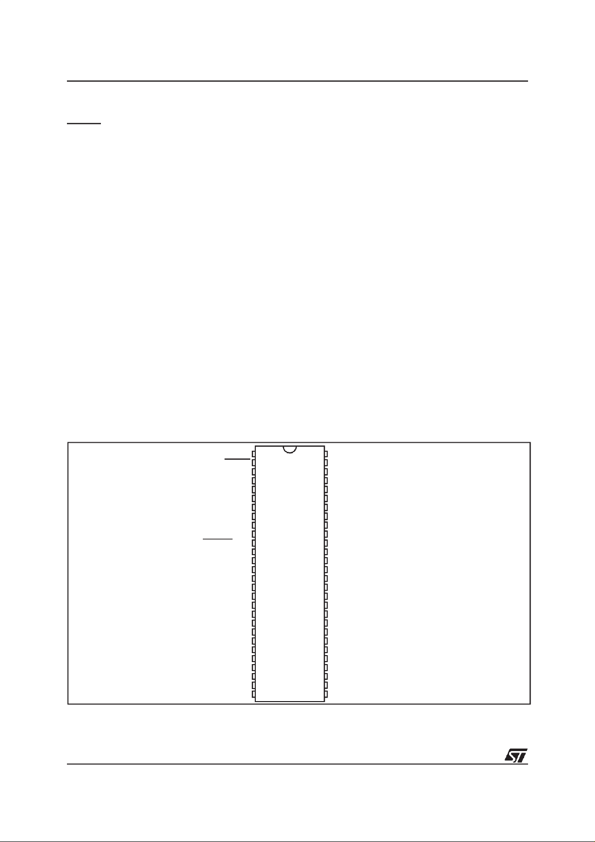
Figure 3. 56-Pin Package Pin-Out
INT7/P2.0
AIN4/P0.2
CSO/RESET0/P3.7
SDI/SDO/P5.1
SCK/INT2/P5.0
V
PP
RESET
P0.7
P0.6
P0.5
P0.4
P0.3
P0.1
P0.0
P3.6
P3.5
P3.4
FB
V
DD
JTDO
WSCF
/WSCR
AVDD3
TEST0
MCFM
JTCK
1
2
3
4
5
6
7
8
9
10
11
12
13
14
15
B
16
G
17
R
18
19
20
21
22
23
24
25
26
27
28
P2.1/INT5/AIN1
56
P2.2/INT0/AIN2
55
54
P2.3/INT6/VS01
53
P2.4/NMI
52
P2.5/AIN3/INT4/VS02
51
OSCIN
50
OSCOUT
49
P4.7/PWM7/EXTRG/STOUT
P4.6/PWM6
48
P4.5/PWM5
47
46
P4.4/PWM4
45
P4.3/PWM3/TSLU/HT
44
P4.2/PWM2
43
P4.1/PWM1
42
P4.0/PWM0
41
VSYNC
40
HSYNC/CSYNC
39
AVDD1
38
PXFM
37
JTRSTO
36
GND
35
AGND
34
CVBS1
33
CVBS2
32
JTMS
31
AVDD2
30
CVBSO
29
TXCF
6/22
Page 7
ST92195B - GENERAL DESCRIPTION
PIN DESCRIPTION (Cont’d)
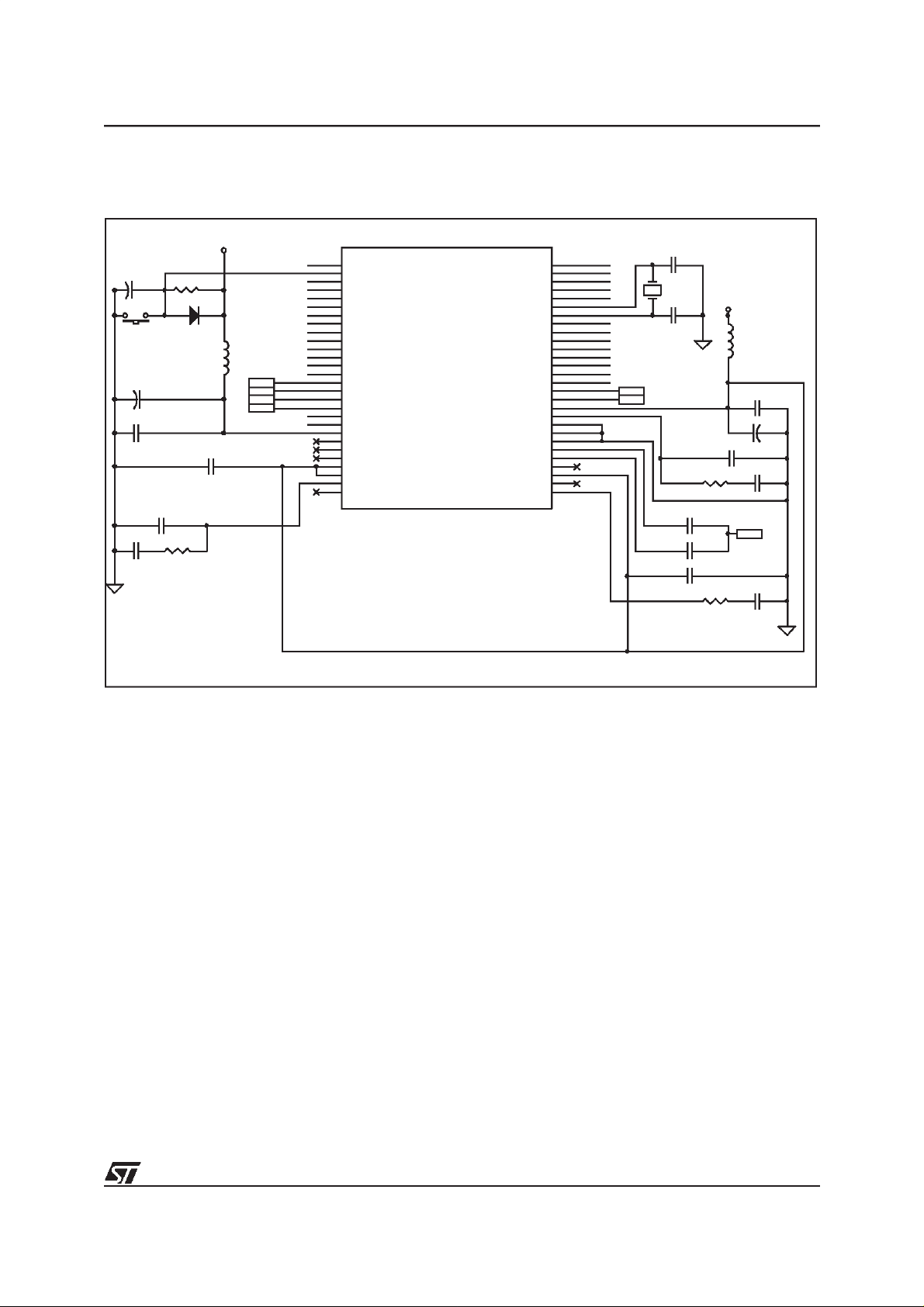
Figure 4. ST92195B Required External components (56-pin package)
+5V
1µF
C2
S1
RST
C4
C6
C11
4.7nF
C13
10µF
100nF
22pF
R3
10k
R1
D1
1N4148
L2
10uH
B
G
R
FB
100nF
C9
5.6k
U1
P20
1 56
P2.0/INT7 P2.1/INT5/AIN1
2
P07
P06
P05
P04
P03
P02
P01
P00
P37
P36
P35
P34
P51
P50
RESETN
3
P0.7
4
P0.6
5
P0.5
6
P0.4
7
P0.3
8
P0.2/AIN4
9
P0.1
10
P0.0
11
P3.7/RESET0/CSO
12
P3.6
13
P3.5
14
P3.4
15
B
16
G
17
R
18
FB
19
P5.1/SDI/SDO
20
P5.0/SCK/INT2
21
VDD
22
JTDO
23
WSCF
24
WSCR
25
AVDD3
26
TEST0
27
MCFM
28
JTCK
SDIP56
ST92195B
P2.2/INT0/AIN2
P2.3/INT6/VS01
P2.5/AIN3/INT4/VS02
P4.7/PWM7/EXTRG/STOUT
P4.3/PWM3/TSLU/HT
HSYNC/CSYNC
P2.4/NMI
OSCIN
OSCOUT
P4.6/PWM6
P4.5/PWM5
P4.4/PWM4
P4.2/PWM2
P4.1/PWM1
P4.0/PWM0
VSYNC
AVDD1
PXFM
JTRST0
GND
AGND
CVBS1
CVBS2
JTMS
AVDD2
CVBSO
TXCF
82pF
VSYNC
HSYNC
C1
Y1
4Mhz
C3
C12
C14
C15
82pF
R2
470nF
82pF
100nF
R4
C8
5.6k
15k
+5V
L1
10uH
C5
100nF
10µF
C7
22pF
4.7nF
C10
CVBS
2.2nF
C16
P21
P22
55
P23
54
P24
53
P25
52
51
50
P47
49
P46
48
P45
47
P44
46
P43
45
P42
44
P41
43
P40
42
41
40
39
38
37
36
35
34
33
32
31
30
29
7/22
Page 8

ST92195B - GENERAL DESCRIPTION
PIN DESCRIPTION (Cont’d)
Figure 5. ST92195B Required External Components (64-pin package)
1µF
C1
S1
RST
C5
10uF
C7
100nF
10k
R1
P5.1
+5V
U1
1
VSS
2
P0.2/AIN4
3
P0.1
4
P0.0
5
P3.7/RESET0/CSO
6
P3.6
7
P3.5
8
P3.4
9
B
10
G
11
R
12
FB
13
P5.1/SDI/SDO
14
P5.0/SCK/INT2
15
VDD
16
JTDO
QFP64
C3
100nF
P05
P03
P06
P07
P04
64
P0.7
P0.6
P0.5
P0.4
P0.3
VDD
MCFM
NC
WSCF
WSCR
AVDD3
TEST0
NC
23
181920212224252627
17
P20
P21
P22
56
55545352515049
57585960616263
RESETN
INT7/P2.0
P2.1/INT5/AIN1
P2.2/INT0/AIN2
ST92195B
JTCK
TXCF
CVBSO
AVDD2
P25
P24
P23
OSCIN
P2.4/NMI
P2.3/INT6/VS01
P2.5/AIN3/INT4/VS02
AGND
CVBS1
CVBS2
JTMS
29
28
C6 100nF
VDD
OSCOUT
EXTRG/SLOUT/P4.7/PWM7
NC
323130
P4.6/PWM6
P4.5/PWM5
P4.4/PWM4
HT/TSLU/P4.3/PWM3
P4.2/PWM2
P4.1/PWM1
P4.0/PWM0
CSYNC/HSYNC
Y1
4Mhz
JTRST0
VSYNC
AVDD1
C2 82pF
C4 82pF
GND
PXFM
GND
NC
48
47
P47
46
P46
45
P45
44
P44
43
P43
42
P42
41
P41
40
P40
39
38
37
36
35
34
33
C8 100nF
R2
5.6k
VSYNC
HSYNC
22pF
C9
C10
4.7nF
D1
1N4148
L1
10uH
P02
P01
P00
P37
P36
P35
P34
B
G
R
FB
P5.0
C15
C14
4.7nF
22pF
C11
100nF
R3
5.6k
C12
100nF
C13
10uF
L2
10uH
+5V
8/22
Page 9

PIN DESCRIPTION (Cont’d)
P0[7:0], P2[5:0], P3[7:4], P4[7:0], P5[1:0]
I/O Port Lines
(Input/Output, TTL or CMOS com-
patible).
28 lines grouped into I/O ports, bit programmable
as general purpose I/O or as Alternate functions
(see I/O section).
Important
logic levels only and arenot true open drain.
1.2.1 I/O Port Alternate Functions.
Each pinof the I/Oports of the ST92195B may assume software programmable Alternate Functions
(see Table 1).
Table 1. ST92195B I/O Port Alternate Function Summary
ST92195B - GENERAL DESCRIPTION
: Note that open-drain outputs are for
Port
Name
P0.0
P0.1 3 9 I/O
P0.2 2 8 AIN4 I A/D Analog Data Input 4
P0.3 63 7 I/O
P0.4 62 6 I/O
P0.5 61 5 I/O
P0.6 60 4 I/O
P0.7 59 3 I/O
P2.0 57 1 INT7 I External Interrupt 7
P2.1 56 56
P2.2 55 55
P2.3 54 54
P2.4 53 53 NMI I Non Maskable Interrupt Input
P2.5 52 52
P3.4 8 14 I/O
P3.5 7 13 I/O
P3.6 6 12 I/O
P3.7 5 11
P4.0 40 42 PWM0 O PWM Output 0
P4.1 41 43 PWM1 O PWM Output 1
P4.2 42 44 PWM2 O PWM Output 2
P4.3 43 45
P4.4 44 46 PWM4 O PWM Output 4
General
Purpose I/O
All ports useable
for general purpose I/O (input,
output or bidirectional)
Pin No.
TQFP64 SDIP56
4 10 I/O
AIN1 I A/D Analog Data Input 1
INT5 I External Interrupt 5
INT0 I External Interrupt 0
AIN2 I A/D Analog Data Input 2
INT6 I External Interrupt 6
VSO1 O Voltage Synthesis Output 1
AIN3 I A/D Analog Data Input 3
INT4 I External Interrupt 4
VSO2 O Voltage Synthesis Output 2
RESET0 O Internal Reset Output
CSO O Composite Sync output
PWM3 O PWM Output 3
TSLU O Translucency Digital Output
HT O Half-tone Output
Alternate Functions
9/22
Page 10

ST92195B - GENERAL DESCRIPTION
Port
Name
P4.5
P4.6 46 48 PWM6 O PWM Output 6
P4.7 47 49
P5.0 14 20
P5.1 13 19
General
Purpose I/O
All ports useable
for general purpose I/O (input,
output or bidirectional)
Pin No.
TQFP64 SDIP56
45 47 PWM5 O PWM Output 5
EXTRG I A/D Converter External Trigger Input
PWM7 O PWM Output 7
STOUT O Standard Timer Output
INT2 I External Interrupt 2
SCK O SPI Serial Clock
SDO O SPI Serial Data Out
SDI I SPI Serial Data In
Alternate Functions
1.2.2 I/O Port Styles
Pins Weak Pull-Up Port Style Reset Values
P0[7:0] no Standard I/O BID / OD / TTL
P2[5,4,3,2] no Standard I/O BID / OD / TTL
P2[1,0] no Schmitt trigger BID / OD / TTL
P3.7 yes Standard I/O AF / PP / TTL
P3[6,5,4] no Standard I/O BID / OD / TTL
P4[7:0] no Standard I/O BID / OD / TTL
P5[1:0] no Standard I/O BID / OD / TTL
Legend:
AF= Alternate Function, BID = Bidirectional, OD = Open Drain
PP = Push-Pull, TTL = TTL Standard Input Levels
How to Read this Table
To configure the I/O ports, use the information in
this table and the Port Bit Configuration Table in
the I/O Ports Chapter ofthe datasheet.
Port Style= the hardware characteristics fixed for
each port line.
Inputs:
– Ifport style = Standard I/O, either TTL or CMOS
input level can be selected by software.
– If port style=Schmitt trigger, selectingCMOS or
TTL inputbysoftwarehasno effect,the input will
always be Schmitt Trigger.
Weak Pull-Up = This column indicates if a weak
pull-up is present or not.
– If WPU =yes, then the WPU can be enabled/dis-
able by software
– If WPU=no,then enabling theWPU bysoftware
has no effect
Alternate Functions (AF) = More than one AF
cannot be assigned to an external pin at the same
time:
An alternate function can be selected as follows.
AF Inputs:
– AF is selected implicitly by enabling the corre-
sponding peripheral. Exception to this are ADC
analog inputs which must be explicitly selected
as AF by software.
10/22
Page 11

PIN DESCRIPTION (Cont’d)
AF Outputs or Bidirectional Lines:
– In the case of Outputs or I/Os, AF is selected
explicitly by software.
Example 1: ADC trigger digital input
AF: EXTRG, Port: P4.7, Port Style: Standard I/O.
Write the port configuration bits (for TTL level):
P4C2.7=1
P4C1.7=0
P4C0.7=1
Enable the ADC trigger by software as described
in the ADC chapter.
Example 2: PWM 0 output
AF: PWM0, Port: P4.0
Write the port configuration bits (for output push-
pull):
P4C2.0=0
P4C1.0=1
P4C0.0=1
ST92195B - GENERAL DESCRIPTION
Example 3: ADC analoginput
AF: AIN1, Port: P2.1, Port style: does not apply to
analog inputs
Write the port configuration bits:
P2C2.1=1
P2C1.1=1
P2C0.1=1
11/22
Page 12

ST92195B - GENERAL DESCRIPTION
1.3 MEMORY MAP
Internal ROM
The ROM memory is mapped in a single continuous area starting at address 0000h in MMU segment 00h.
Device Size
Start
Address
ST92195B1/B2/B3 32K 0000h 7FFFh
ST92195B4/B5 48K 0000h BFFFh
ST92195B6 56K 0000h DFFFh
ST92195B7 64K 0000h FFFFh
End
Address
Figure 6. ST92195B Memory Map
max. 8 Kbytes
TDSRAM
229FFFh
228000h
SEGMENT 22h
64 Kbytes
SEGMENT 21h
64 Kbytes
Internal RAM, 256 bytes
The internal RAM is mapped in MMU segment
20h; from address FF00h to FFFFh.
Internal TDSRAM
The Internal TDSRAM is mapped starting at address 8000h in MMU segment 22h. It isa fully static memory.
Device Size
Start
Address
ST92195B1 2K 8000h 87FFh
ST92195B2/B3/B4 6K 8000h 97FFh
ST92195B5/B6/B7 8K 8000h 9FFFh
Reserved
Reserved
Reserved
Reserved
22FFFFh
22C000h
22BFFFh
228000h
227FFFh
224000h
223FFFh
220000h
21FFFFh
PAGE 91 - 16 Kbytes
PAGE 90 - 16 Kbytes
PAGE 89 - 16 Kbytes
PAGE 88 - 16 Kbytes
End
Address
Internal
RAM
256 bytes
20FFFFh
20FF00h
SEGMENT 20h
64 Kbytes
SEGMENT 0
64 Kbytes
Reserved
Reserved
Reserved
Internal ROM
max. 64 Kbytes
210000h
20FFFFh
20C000h
20BFFFh
208000h
207FFFh
204000h
203FFFh
200000h
00FFFFh
00C000h
00BFFFh
008000h
007FFFh
004000h
003FFFh
000000h
PAGE 83 - 16 Kbytes
PAGE 82 - 16 Kbytes
PAGE 81 - 16 Kbytes
PAGE 80 - 16 Kbytes
PAGE 3 - 16 Kbytes
PAGE 2 - 16 Kbytes
PAGE 1 - 16 Kbytes
PAGE 0 - 16 Kbytes
12/22
Page 13

ST92195B - ELECTRICAL CHARACTERISTICS
2 ELECTRICAL CHARACTERISTICS
ABSOLUTE MAXIMUM RATINGS
Symbol Parameter Value Unit
V
DD
V
SSA
V
DDA
V
I
V
AI
V
O
T
STG
I
INJ
Note: Stress above those listed as “Absolute maximum ratings” may cause permanent damage to the device. This is astress rating only and
functional operation of the device at these conditions is not implied. Exposure to maximum rating conditions for extended periods may affect
device reliability.
Supply Voltage VSS- 0.3 to VSS+ 7.0 V
Analog Ground VSS- 0.3 to VSS+ 0.3 V
Analog Supply Voltage VDD-0.3 to VDD+0.3 V
Input Voltage VSS- 0.3 to VDD+0.3 V
- 0.3 to VDD+0.3
V
Analog Input Voltage (A/D Converter)
V
SS
SSA
- 0.3 to V
DDA
+0.3
V
Output Voltage VSS- 0.3 to VDD+ 0.3 V
Storage Temperature - 55 to + 150 °C
Pin Injected Current
-5to+5
mA
Maximum Accumulated Pin
Injected Current In Device
-50to+50
mA
RECOMMENDED OPERATING CONDITIONS
Symbol Parameter
T
A
V
DD
V
DDA
f
OSCE
f
OSCI
Operating Temperature 0 70 °C
Supply Voltage 4.5 5.5 V
Analog Supply Voltage (PLL) 4.5 5.5 V
External Oscillator Frequency 3.3 8.7 MHz
Internal Clock Frequency (INTCLK) 24 MHz
Value
Min. Max.
Unit
13/22
Page 14

ST92195B - ELECTRICAL CHARACTERISTICS
DC ELECTRICAL CHARACTERISTICS
(VDD= 5V +/-10%; TA= 0 to 70°C; unless otherwise specified)
Symbol Parameter Test Conditions
V
V
V
V
V
V
V
V
V
V
V
V
V
V
V
IHCK
ILCK
IH
IL
IH
IL
IHRS
ILRS
HYRS
IHY
IHVH
ILVH
HYHV
OH
OL
Clock In high level External clock 0.7 V
Clock in low level External clock 0.3 V
Input high level TTL 2.0 V
Input low level TTL 0.8 V
Input high level CMOS 0.8 V
Input low level CMOS 0.2 V
Reset in high level 0.7 V
Reset in low level 0.3 V
Reset in hysteresis 0.3 V
P2.(1:0) input hysteresis 0.9 V
HSYNC/VSYNC input high level 0.7 V
HSYNC/VSYNC input low level 0.3 V
HSYNC/VSYNC input hysteresis 0.5 V
Output high level Push-pull Ild=-0.8mA VDD-0.8 V
Output low level Push-pull ld=+1.6mA 0.4 V
bidir. state
I
WPU
I
LKIO
I
LKRS
I
LKAD
I
LKOS
Weak pull-up current
I/O pin input leakage current 0<VIN<V
Reset pin input 0<VIN<V
A/D pin input leakage current alternate funct. op. drain -10 +10 µA
OSCIN pin input leakage current 0<VIN<V
VOL=3V
=7V
V
OL
DD
DD
DD
Value
Min. Max.
DD
DD
DD
DD
Unit
DD
DD
DD
DD
50
350
-10 +10 µA
-10 +10 µA
-10 +10 µA
V
V
V
V
V
V
V
V
µA
14/22
Page 15

ST92195B - ELECTRICAL CHARACTERISTICS
AC ELECTRICAL CHARACTERISTICS
PIN CAPACITANCE
(VDD= 5V +/-10%; TA= 0 to 70°C; unless otherwise specified))
Symbol Parameter Conditions
C
IO
Pin Capacitance Digital Input/Output 10 pF
Value
min max
Unit
CURRENT CONSUMPTION
(VDD= 5V +/-10%; TA= 0 to 70°C; unless otherwise specified)
Symbol Parameter Condition s
I
DD1
I
DDA1
I
DD2
I
DDA2
Notes:
1. Port 0isconfigured inpush-pull output mode (output ishigh).Ports 2, 3, 4 and5 are configured in bi-directional weakpull-up mode resistor.
The external CLOCK pin(OSCIN) is driven by a square wave external clock at 8 MHz. The internal clock prescaler is in divide-by-1 mode.
2. The CPU is fed by a 24 MHz frequency issued by the Main Clock Controller. VSYNC is tied to
All peripherals working including Display.
3. The CPU is fed by a 24 MHz frequency issued by the Main Clock Controller. VSYNC is tied to
The TDSRAM interface and the Slicers are working; the Display controller is not working.
4. VSYNC and HSYNC tied to
Run Mode Current notes 1,2; all On 70 100 mA
Run Mode Analog Current
DDA
)
(pin V
Timing Controller On 35 50 mA
HALT Mode Current notes 1,4 10 100 µA
HALTMode Analog Current
(pin V
)
DDA
V
. External CLOCK pin (OSCIN) is hold low. All peripherals are disabled.
SS
notes 1,4 40 100 µA
min typ. max
V
V
Value
, HSYNCis driven by a 15625Hz clock.
SS
, HSYNCis driven by a 15625Hz clock.
SS
Unit
EXTERNAL INTERRUPT TIMING TABLE (rising or falling edge mode)
(VDD= 5V +/-10%; TA= 0 to 70°C; unless otherwise specified))
Symbol Parameter
T
wLR
T
wHR
TpC is the INTCLK clock period.
low level pulse width TpC+12 95 ns
high level pulse width TpC+12 95 ns
Conditions Value Unit
INTCLK=24 MHz. min max
15/22
Page 16

ST92195B - ELECTRICAL CHARACTERISTICS
AC ELECTRICAL CHARACTERISTICS (Cont’d)
SPI TIMING TABLE
(VDD= 5V +/-10%; TA= 0 to 70°C; Cload= 50pF)
Symbol Parameter Condition
T
sDI
T
hDI
T
dOV
T
hDO
T
wSKL
T
wSKH
(1) TpC is the OSCIN clock period; TpMC is the “Main Clock Frequency” period.
Input Data Set-up Time tbd ns
Input Data Hold Time (1) OSCIN/2 as internal Clock 1INTCLK +100ns ns
SCK to Output Data Valid tbd ns
Output Data Hold Time tbd ns
SCK Low Pulse Width tbd ns
SCK High Pulse Width tbd ns
Value
min max
Unit
SKEW CORRECTOR TIMING TABLE
(VDD= 5V +/-10%, TA= 0 to 70°C, unless otherwise specified)
Symbol Parameter Conditions
T
jskw
(*) The OSD jitter is measured from leading edge to leading edge of asingle character row on consecutive TV lines. The value is an envelope
of 100 fields
Jitter on RGB output 36 MHz Skew corrector clock frequency 5* ns
max
Value
Unit
16/22
Page 17

ST92195B - ELECTRICAL CHARACTERISTICS
AC ELECTRICAL CHARACTERISTICS (Cont’d)
OSD DAC CHARACTERISTICS (ROM DEVICES ONLY)
(VDD= 5V +/-10%, TA= 0 to 70°C, unless otherwise specified).
Symbol Parameter Conditions
Output impedance: FB,R,G,B 300 500 700 Ohm
Output voltage: FB,R,G,B
code= 111 1.000 1.250 V
code= 011 0.450 0.500 V
code= 000 0.025 0.080 V
FB= 1 2.4 2.7 3.4 V
FB= 0 0 0.025 0.080 V
Global voltage accuracy +/-5 %
Cload= 20pF
RL = 100K
min typical max
OSD DAC CHARACTERISTICS (EPROM AND OTP DEVICES ONLY)
(VDD= 5V +/-10%, TA= 0 to 70°C, unless otherwise specified).
Symbol Parameter Conditions
Output impedance: FB,R,G,B 300 500 700 Ohm
Output voltage: FB,R,G,B
code= 111 1.100 1.400 V
code= 011 0.600 0.800 V
code= 000 0.200 0.350 V
FB=1 V
FB=0 0.400 V
Global voltage accuracy +/-5 %
Cload= 20pF
RL = 100K
min typical max
-0.8 V
DD
Value
Value
Unit
Unit
17/22
Page 18

ST92195B - ELECTRICAL CHARACTERISTICS
AC ELECTRICAL CHARACTERISTICS (Cont’d)
A/D CONVERTER, EXTERNAL TRIGGER TIMING TABLE
(VDD= 5V +/-10%; TA= 0 to 70°C; unless otherwise specified
Symbol Parameter
T
low
T
high
T
ext
T
str
Pulse Width
Pulse Distance ns
Period/fast Mode
Start Conversion Delay 0.5 1.5 INTCLK
OSCIN divide by
2;min/max
OSCIN divide
by 1; min/max
Value
min max
1.5
INTCLK
78+1
INTCLK
Core Clock issued by Timing Controller
T
low
T
high
T
ext
T
str
Pulse Width ns
Pulse Distance ns
Period/fast Mode µs
Start Conversion Delay ns
A/D CONVERTER. ANALOG PARAMETERS TABLE
(VDD= 5V +/-10%; TA= 0 to 70°C; unless otherwise specified))
Parameter
typ (*) min max (**)
Analog Input Range V
Conversion Time Fast/Slow 78/138 INTCLK (1,2)
Sample Time Fast/Slow 51.5/87.5 INTCLK (1)
Power-up Time 60 µs
Resolution 8 bits
Differential Non Linearity 1.5 2.5 LSBs (4)
Integral Non Linearity 2 3 LSBs (4)
Absolute Accuracy 2 3 LSBs (4)
Input Resistance 1.5 Kohm (3)
Hold Capacitance 1.92 pF
Value Unit
SS
V
DD
V
Unit
ns
µs
Note
Notes: (*) The values are expected at 25 Celsius degrees with VDD=5V
(**) ’LSBs’, as used here, as a value of
(1) @ 24 MHz external clock
(2) including Sample time
(3) it must be considered as the on-chip series resistance before the sampling capacitor
(4) DNL ERROR=max {[V(i) -V(i-1)] / LSB-1} INL ERROR= max {[V(i) -V(0)] / LSB-i}
ABSOLUTE ACCURACY= overall max conversion error
V
/256
DD
18/22
Page 19

ST92195B - GENERAL INFORMATION
3 GENERAL INFORMATION
3.1 PACKAGE MECHANICAL DATA
Figure 7. 56-Pin Shrink Plastic Dual In Line Package, 600-mil Width
Figure 8. 64-Pin Thin Quad Flat Package
L1
L
Dim.
A 6.35 0.250
A1 0.38 0.015
A2 3.18 4.95 0.125 0.195
b 0.41 0.016
b2 0.89 0.035
C 0.20 0.38 0.008 0.015
D 50.29 53.21 1.980 2.095
E 15.01 0.591
E1 12.32 14.73 0.485 0.580
e 1.78 0.070
eA 15.24 0.600
eB 17.78 0.700
L 2.92 5.08 0.115 0.200
PDIP56S
N56
Dim
A 1.60 0.063
A1 0.05 0.15 0.002 0.006
A2 1.35 1.40 1.45 0.053 0.055 0.057
B 0.30 0.37 0.45 0.012 0.015 0.018
C 0.09 0.20 0.004 0.008
D 16.00 0.630
D1 14.00 0.551
D3 12.00 0.472
E 16.00 0.630
E1 14.00 0.551
E3 12.00 0.472
e 0.80 0.031
K 0° 3.5° 7°
L 0.45 0.60 0.75 0.018 0.024 0.030
L1 1.00 0.039
N 64 ND 16 NE 16
K
mm inches
Min Typ Max Min Typ Max
Number of Pins
mm inches
Min Typ Max Min Typ Max
Number of Pins
19/22
Page 20

ST92195B - GENERAL INFORMATION
PACKAGE MECHANICAL DATA (Cont’d)
Figure 9. 56-Pin Shrink Ceramic Dual In Line Package, 600-mil Width
Dim.
A 4.17 0.164
A1 0.76 0.030
B 0.38 0.46 0.56 0.015 0.018 0.022
B1 0.76 0.89 1.02 0.030 0.035 0.040
C 0.23 0.25 0.38 0.009 0.010 0.015
D 50.04 50.80 51.56 1.970 2.000 2.030
D1 48.01 1.890
E1 14.48 14.99 15.49 0.570 0.590 0.610
e 1.78 0.070
G 14.12 14.38 14.63 0.556 0.566 0.576
G1 18.69 18.95 19.20 0.736 0.746 0.756
G2 1.14 0.045
G3 11.05 11.30 11.56 0.435 0.445 0.455
G4 15.11 15.37 15.62 0.595 0.605 0.615
CDIP56SW
L 2.92 5.08 0.115 0.200
S 1.40 0.055
N56
mm inches
Min Typ Max Min Typ Max
Number of Pins
Figure 10. 64-Pin Ceramic Quad Flat Package
Dim
A 3.27 0.129
A1 0.50 0.020
B 0.30 0.35 0.45 0.012 0.014 0.018
C 0.13 0.15 0.23 0.005 0.006 0.009
D 16.65 17.20 17.75 0.656 0.677 0.699
D1 13.57 13.97 14.37 0.534 0.550 0.566
D3 12.00 0.472
e 0.80 0.031
G 12.70 0.500
G2 0.96 0.038
L 0.35 0.80 0.014 0.031
0 8.31 0.327
N64CQFP064W
mm inches
Min Typ Max Min Typ Max
Number of Pins
20/22
Page 21

ST92195B - GENERAL INFORMATION
3.2 ORDERING INFORMATION
Each device is available for production in a user
programmable version (OTP) as well as in factory
coded version(ROM). OTP devices areshipped to
customer with a default blank content FFh, while
ROM factorycoded parts contain the code sentby
customer. The common EPROM versions for debugging and prototyping features the maximum
memory size and peripherals of the family. Care
must be taken to only use resources available on
the target device.
Figure 11. ROM Factory Coded Device Types
DEVICE
PACKAGE
TEMP.
RANGE
XXX/
Code name (defined by STMicroelectronics)
1= standard 0 to +70 °C
B= Plastic DIP56
T= Plastic TQFP64
ST92195B1
ST92195B2
ST92195B3
ST92195B4
ST92195B5
ST92195B6
ST92195B7
3.2.1 Transfer Of Customer Code
Customer code is made up of the ROM contents
and the list of the selected options (if any). The
ROM contents are to be sent on diskette, or by
electronic means, with the hexadecimal file generated by the development tool. All unused bytes
must be set to FFh.
Figure 12. OTP User Programmable Device Types
DEVICE PACKAGE
TEMP.
RANGE
XXX/
Code name (defined by STMicroelectronics)
1= 0 to +70 °C
B= Plastic DIP56
T= Plastic TQFP64
ST92T195B7
Figure 13. EPROM User Programmable Device Types
DEVICE
PACKAGE
TEMP.
RANGE
0= 25 °C
B= Ceramic DIP 56 pin
T= Ceramic QFP 64 pin
ST92E195B7
21/22
Page 22

ST92195B - GENERAL INFORMATION
Notes:
Information furnished is believed to be accurate and reliable. However, STMicroelectronics assumes no responsibility for the consequences
of useof suchinformation norforany infringement ofpatents or other rights ofthirdparties which may result from itsuse. No license isgranted
by implication or otherwise under any patent or patent rights of STMicroelectronics. Specifications mentioned in this publication are subject
to change without notice. This publication supersedes and replaces all information previously supplied. STMicroelectronics products are not
authorized for use as critical components in life support devices or systems without the express written approval of STMicroelectronics.
The ST logo is a registered trademark of STMicroelectronics
2
Purchase of I
Australia - Brazil - China - Finland - France - Germany - Hong Kong -India - Italy - Japan - Malaysia - Malta - Morocco - Singapore - Spain
C Components by STMicroelectronics conveys a license under the Philips I2C Patent. Rights to use these components in an
2
C system is granted provided that the system conforms to the I2C Standard Specification as defined by Philips.
I
2000 STMicroelectronics - All Rights Reserved.
STMicroelectronics Group of Companies
Sweden - Switzerland - United Kingdom - U.S.A.
http://www.st.com
22/22
 Loading...