

Datasheet ST7FSCR1R4, ST7FSCR1E4, ST7SCRDIE, ST7SCR1E4, ST7SCR1R4 Datasheet (SGS Thomson Microelectronics)
...Page 1
Rev. 1.3
March 2003 1/102
ST7SCR
8-BIT LOW-POWER, FULL-SPEED USB MCU WITH 16K
FLASH , 768 RAM, SMARTCARD I/F, TIMER
■ Memories
– Up to 16K of ROM or High Density Flash (HD-
Flash) program memory wi th read/write protection, HDFlash In-Circuit and In-Application
Programming. 100 write/erase cycles guaranteed, data retention: 20 years at 55°C
– Up to 768 bytes of RAM in cluding up to 128
bytes stack and 256 bytes USB buffer
■ Clock , Res et and Supp ly M a nagemen t
– Low Voltage Reset
– 2 power saving modes: Halt and Wait modes
– PLL for generating 48 MHz USB clock using a
4 MHz crystal
■ Interrupt Management
– Nested Interrupt Controller
■ USB (Universal Serial Bus) Interface
– 256-byte buffer for full speed bulk, control and
interrupt transfer types compliant with USB
specification (version 2.0)
– On-Chip 3.3V USB voltage regulator and
transceivers with software power-down
– 7 USB Endpoints:
One 8-byte Bidirectional Control Endpoint
One 64-byte In Endpoint,
One 64-byte Out Endpoint
Four 8-byte In Endpoints
■ 35 or 4 I/O ports:
– Up to 4 LED outputs with software program -
mable constant current (3 or 7 mA).
– 2 General purpose I/Os program mable as in-
terru p ts
– Up to 8 line inputs programmable as interrupts
– Up to 20 Outputs
– 1 line assigned by default as st atic input after
reset
■ ISO7816-3 UART Interface:
– 4 Mhz Clock generation
– Synchronous/Asynchronous protocols (T=0,
T=1)
– Automatic retry on parity error
– Programmable Baud rate from 372 clock puls-
es up to 11.625 clock pulses (D=32/F=372)
– Card Insertion/Removal Detection
■ Smartcard Power Suppl y:
– Selectable card V
CC
1.8V, 3V, and 5V
– Internal Step-up converter for 5V supplied
Smartcards (with a current of up to 55mA) us-
ing only two external components.
– Programmable Smartcard Internal Voltage
Regulator (1.8V to 3.0V) with current overload
protection and 4 KV ESD protection (Human
Body Model) for all Smartcard Interface I/Os
■ One 8-bit Timer
– Time Base Unit (TBU) for generating periodic
interrupts.
■ Development Tools
– Full hardware/software development package
Table 1. Device Summa ry
TQFP64 14x14
SO24
Features ST7FSCR1R4 ST7SCR1R4 ST7FSCR1E4 ST7SCR1E4
Program memory 16K FLASH 16K ROM 16K FLASH 16K ROM
User RAM (stack) - bytes 768 (128)
Peripherals USB Full-Speed (7 Ep), TBU, Watchdog timer, ISO7816-3 Interface
Operating Supply 4.0 to 5.5V
Package TQFP64 SO24
CPU Frequency 4 or 8 Mhz
Operating temperature 0°C to +70°C
1
Page 2

Table of Cont ents
102
2/102
ST7SCR . . . . . . . . . . . . . . . . . . . . . . . . . . . . . . . . . . . . . . . . . . . . . . . . . . . . . . 1
1 INTRODUCTION . . . . . . . . . . . . . . . . . . . . . . . . . . . . . . . . . . . . . . . . . . . . . . . . . . . . . . . . . . . . . . 4
2 PIN DESCRIPTION . . . . . . . . . . . . . . . . . . . . . . . . . . . . . . . . . . . . . . . . . . . . . . . . . . . . . . . . . . . . 5
3 REGISTER & MEM ORY MAP . . . . . . . . . . . . . . . . . . . . . . . . . . . . . . . . . . . . . . . . . . . . . . . . . . . 11
4 FLASH PROGRAM MEMORY . . . . . . . . . . . . . . . . . . . . . . . . . . . . . . . . . . . . . . . . . . . . . . . . . . 14
4.1 INTRODUCTION . . . . . . . . . . . . . . . . . . . . . . . . . . . . . . . . . . . . . . . . . . . . . . . . . . . . . . . 14
4.2 MAIN FEATURES . . . . . . . . . . . . . . . . . . . . . . . . . . . . . . . . . . . . . . . . . . . . . . . . . . . . . . 14
4.3 STRUCTURE . . . . . . . . . . . . . . . . . . . . . . . . . . . . . . . . . . . . . . . . . . . . . . . . . . . . . . . . . . 14
4.4 ICP (IN-CIRCUIT PR OGRAMMING) . . . . . . . . . . . . . . . . . . . . . . . . . . . . . . . . . . . . . . . . 15
4.5 IAP (IN-APPLICATION PROGRAMMING) . . . . . . . . . . . . . . . . . . . . . . . . . . . . . . . . . . . 15
4.6 PROGRAM MEMORY READ-O UT PROTECTION . . . . . . . . . . . . . . . . . . . . . . . . . . . . . 16
5 CENTRAL PROCESSING UNIT . . . . . . . . . . . . . . . . . . . . . . . . . . . . . . . . . . . . . . . . . . . . . . . . . 17
5.1 INTRODUCTION . . . . . . . . . . . . . . . . . . . . . . . . . . . . . . . . . . . . . . . . . . . . . . . . . . . . . . . 17
5.2 MAIN FEATURES . . . . . . . . . . . . . . . . . . . . . . . . . . . . . . . . . . . . . . . . . . . . . . . . . . . . . . 17
5.3 CPU REGISTERS . . . . . . . . . . . . . . . . . . . . . . . . . . . . . . . . . . . . . . . . . . . . . . . . . . . . . . 17
6 SUPPLY, RESET AND CLOCK MANAGEMENT . . . . . . . . . . . . . . . . . . . . . . . . . . . . . . . . . . . . 20
6.1 CLOCK SYSTEM . . . . . . . . . . . . . . . . . . . . . . . . . . . . . . . . . . . . . . . . . . . . . . . . . . . . . . . 20
6.2 RESET SEQUENCE MANAGER (RSM) . . . . . . . . . . . . . . . . . . . . . . . . . . . . . . . . . . . . . 22
7 INTERRUPTS . . . . . . . . . . . . . . . . . . . . . . . . . . . . . . . . . . . . . . . . . . . . . . . . . . . . . . . . . . . . . . . 23
7.1 INTRODUCTION . . . . . . . . . . . . . . . . . . . . . . . . . . . . . . . . . . . . . . . . . . . . . . . . . . . . . . . 23
7.2 MASKING AND PROCESSING FLOW . . . . . . . . . . . . . . . . . . . . . . . . . . . . . . . . . . . . . . 23
7.3 INTERRUPTS AND LOW POWER MODES . . . . . . . . . . . . . . . . . . . . . . . . . . . . . . . . . . 25
7.4 CONCURRENT & NESTED MANAGEMENT . . . . . . . . . . . . . . . . . . . . . . . . . . . . . . . . . 25
7.5 INTERRUPT REGISTER DESCRIPTION . . . . . . . . . . . . . . . . . . . . . . . . . . . . . . . . . . . . 26
8 POWER SAVING MODES . . . . . . . . . . . . . . . . . . . . . . . . . . . . . . . . . . . . . . . . . . . . . . . . . . . . . 28
8.1 INTRODUCTION . . . . . . . . . . . . . . . . . . . . . . . . . . . . . . . . . . . . . . . . . . . . . . . . . . . . . . . 28
8.2 WAIT MODE . . . . . . . . . . . . . . . . . . . . . . . . . . . . . . . . . . . . . . . . . . . . . . . . . . . . . . . . . . 28
8.3 HALT MODE . . . . . . . . . . . . . . . . . . . . . . . . . . . . . . . . . . . . . . . . . . . . . . . . . . . . . . . . . . 29
9 I/O PORTS . . . . . . . . . . . . . . . . . . . . . . . . . . . . . . . . . . . . . . . . . . . . . . . . . . . . . . . . . . . . . . . . . . 30
9.1 INTRODUCTION . . . . . . . . . . . . . . . . . . . . . . . . . . . . . . . . . . . . . . . . . . . . . . . . . . . . . . . 30
9.2 FUNCTIONAL DESCRIPTION . . . . . . . . . . . . . . . . . . . . . . . . . . . . . . . . . . . . . . . . . . . . 30
9.3 I/O PORT IMPLEMENTATION . . . . . . . . . . . . . . . . . . . . . . . . . . . . . . . . . . . . . . . . . . . . 31
9.4 REGISTER DESCRIPTION . . . . . . . . . . . . . . . . . . . . . . . . . . . . . . . . . . . . . . . . . . . . . . . 34
10 MISCEL LANEOUS REGISTERS . . . . . . . . . . . . . . . . . . . . . . . . . . . . . . . . . . . . . . . . . . . . . . . 36
11 LEDs . . . . . . . . . . . . . . . . . . . . . . . . . . . . . . . . . . . . . . . . . . . . . . . . . . . . . . . . . . . . . . . . . . . . . 39
12 ON-CHIP PERIPHERALS . . . . . . . . . . . . . . . . . . . . . . . . . . . . . . . . . . . . . . . . . . . . . . . . . . . . . 40
12.1 WATCHDOG TIMER (WDG) . . . . . . . . . . . . . . . . . . . . . . . . . . . . . . . . . . . . . . . . . . . . . . 40
12.2 TIME BASE UNIT (TBU) . . . . . . . . . . . . . . . . . . . . . . . . . . . . . . . . . . . . . . . . . . . . . . . . . 42
12.3 USB INTERFACE (USB) . . . . . . . . . . . . . . . . . . . . . . . . . . . . . . . . . . . . . . . . . . . . . . . . . 44
12.4 SMARTCARD INTERFACE (CRD) . . . . . . . . . . . . . . . . . . . . . . . . . . . . . . . . . . . . . . . . . 55
1
Page 3

Table of Cont ents
3/102
13 INSTRU CTION SET . . . . . . . . . . . . . . . . . . . . . . . . . . . . . . . . . . . . . . . . . . . . . . . . . . . . . . . . . 70
13.1 ST7 ADDRESSING MODES . . . . . . . . . . . . . . . . . . . . . . . . . . . . . . . . . . . . . . . . . . . . . . 70
13.2 INSTRUCTION GROUPS . . . . . . . . . . . . . . . . . . . . . . . . . . . . . . . . . . . . . . . . . . . . . . . . 73
14 ELECTRICAL CHARACTERISTICS . . . . . . . . . . . . . . . . . . . . . . . . . . . . . . . . . . . . . . . . . . . . . 76
14.1 ABSOLUTE MAXIMUM RATINGS . . . . . . . . . . . . . . . . . . . . . . . . . . . . . . . . . . . . . . . . . 76
14.2 RECOMMENDED OPERATING CONDITIONS . . . . . . . . . . . . . . . . . . . . . . . . . . . . . . . 77
14.3 SUPPLY AND RESET CHARACTERISTICS . . . . . . . . . . . . . . . . . . . . . . . . . . . . . . . . . 79
14.4 CLOCK AND TIMING CHARACTERISTICS . . . . . . . . . . . . . . . . . . . . . . . . . . . . . . . . . . 79
14.5 MEMORY CHARACTERISTICS . . . . . . . . . . . . . . . . . . . . . . . . . . . . . . . . . . . . . . . . . . . 82
14.6 SMARTCARD SUPPLY SUPERVISOR ELECTRICAL CHARACTERISTICS . . . . . . . . 82
14.7 EMC CHARACTERIST ICS . . . . . . . . . . . . . . . . . . . . . . . . . . . . . . . . . . . . . . . . . . . . . . . 84
14.8 COMMUNICATION INTERFACE CHARACTERISTICS . . . . . . . . . . . . . . . . . . . . . . . . . 89
15 PACKAGE CHARACTERISTICS . . . . . . . . . . . . . . . . . . . . . . . . . . . . . . . . . . . . . . . . . . . . . . . 90
15.1 PACKAGE MECHANICAL DATA . . . . . . . . . . . . . . . . . . . . . . . . . . . . . . . . . . . . . . . . . . 90
16 DEVICE CONFIGURATION AND ORDERING INFORMATION . . . . . . . . . . . . . . . . . . . . . . . . 92
16.1 DEVICE ORDERING INFORMATION AND TRANSFER OF CUSTOMER CODE . . . . . 93
16.2 DEVELOPMENT T OOLS . . . . . . . . . . . . . . . . . . . . . . . . . . . . . . . . . . . . . . . . . . . . . . . . 95
16.3 ST7 APPLICATION NOTES . . . . . . . . . . . . . . . . . . . . . . . . . . . . . . . . . . . . . . . . . . . . . . 96
17 SUMMARY OF CHANGES . . . . . . . . . . . . . . . . . . . . . . . . . . . . . . . . . . . . . . . . . . . . . . . . . . . . 98
ERRAT A SHEET . . . . . . . . . . . . . . . . . . . . . . . . . . . . . . . . . . . . . . . . . . . . . . 99
18 SILICON IDENTIFICATION . . . . . . . . . . . . . . . . . . . . . . . . . . . . . . . . . . . . . . . . . . . . . . . . . . . . 99
19 REFERENCE SPECIFICATION . . . . . . . . . . . . . . . . . . . . . . . . . . . . . . . . . . . . . . . . . . . . . . . . 99
20 SILICON LIMITATIONS . . . . . . . . . . . . . . . . . . . . . . . . . . . . . . . . . . . . . . . . . . . . . . . . . . . . . . 99
20.1 UNEXPECTED RESET FETCH . . . . . . . . . . . . . . . . . . . . . . . . . . . . . . . . . . . . . . . . . . . 99
20.2 USB: TWO CO NSECUTIVE SETUP TOKENS . . . . . . . . . . . . . . . . . . . . . . . . . . . . . . . . 99
20.3 USB BUFFER SHARED MEMORY ACCESS . . . . . . . . . . . . . . . . . . . . . . . . . . . . . . . . 100
20.4 WDG (WATCHDOG) LIMITATIONS . . . . . . . . . . . . . . . . . . . . . . . . . . . . . . . . . . . . . . . 100
20.5 SUPPLY CURRENT IN HALT MODE (SUSPEND) LIMITATIONS . . . . . . . . . . . . . . . . 100
20.6 START-UP . . . . . . . . . . . . . . . . . . . . . . . . . . . . . . . . . . . . . . . . . . . . . . . . . . . . . . . . . . . 100
20.7 I/O PORT INPUT HIGH LEVEL (VIH) . . . . . . . . . . . . . . . . . . . . . . . . . . . . . . . . . . . . . . 101
21 Devic e Marking . . . . . . . . . . . . . . . . . . . . . . . . . . . . . . . . . . . . . . . . . . . . . . . . . . . . . . . . . . . . 101
22 ERRATA SHEET ReVISION History . . . . . . . . . . . . . . . . . . . . . . . . . . . . . . . . . . . . . . . . . . . 101
1
To obtain the most recent version of this datasheet,
please check at www.st.com>products>technical liter ature>datasheet
Please note that an errata sheet can be found at the end of this document on
page 99.
Page 4
ST7SCR
4/102
1 INTRODUCTION
The ST7SCR and ST7FSCR devices are members of the ST7 microcontroller family designed for
USB applications. All devices are based on a common industry-standard 8-bit core, feat uring an enhanced instruction set.
The ST7SCR ROM devices are factory-programmed and are not reprogrammable.
The ST7FSCR versions feature dual-voltage
Flash memory with Flash Programming capability.
They operate at a 4MHz external oscillator frequency.
Under software control, all devices c an be place d
in WAIT or HALT mode, reducing power consumption when the application is in idle or stand-by
state.
The enhanced instruction set and addressing
modes of the ST7 offer both power and flexibility to
software developers, enabling the design of highly
efficient and compact application code. In addition
to standard 8-bit data management, all ST7 microcontrollers feature true bit manipulation, 8x8 un-
signed multiplication and indirect addressing
modes.
The devices include an ST7 Core, up to 16 Kbytes
of program memory, up to 512 bytes of user RAM,
up to 35 I/O lines and the following on-chip peripherals:
– USB full speed interface with 7 endpoints, pro-
grammable in/out configuration and embedded
3.3V voltage regulator and transceivers (no external components are needed).
– ISO7 816-3 UA RT interface with Programmable
Baud rate from 372 clock pulses up to 11.625
clock pulses
– Smartcard Supply Block able to provide pro-
grammable supply voltage and I/O voltage levels
to the smartcards
– Low voltage reset ensuring proper power-on or
power-off of the device (selectable by option)
– Watc hdog Timer
– 8-bit Timer (TBU)
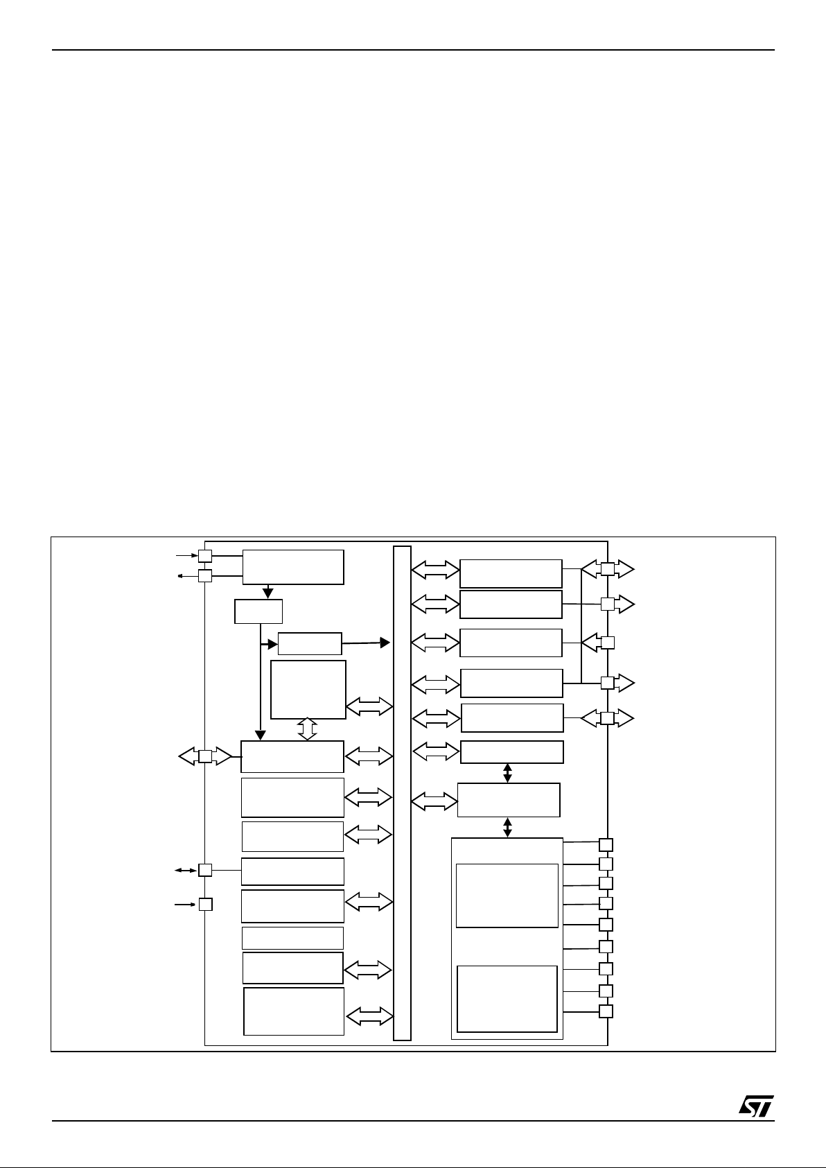
Figure 1. ST7SCR Block Diagram
8-BIT CO RE
ALU
ADDRESS AND DATA BUS
OSCIN
OSCOUT
PA6
4MHz
CONTROL
RAM
(512 Bytes)
PROGRAM
(16K Byt es)
MEMORY
8-BIT TIMER
LVD
V
PP
USBDP
USBDM
USBVCC
PORT C
PC[7:0]
PB[7:0]
PA[5:0]
SUPPLY
MANAG E R
PLL
OSCILLATOR
USB
PORT B
PORT A
USB
DATA
BUFFER
(256 bytes)
DIVIDER
8 MHz
3V/1.8V Vreg
DC/DC
CRDDET
CRDIO
CRDC4
CRDC8
CRDRST
CRDCLK
PD[7:0]
ISO7816 UART
PORT D
CONVERTER
CRDVCC
SELF
WATCHDOG
LED
LED[3:0]
or 4 MHz
48 MHz
DIODE
1
Page 5
ST7SCR
5/102
2 PIN DESCRIPTION
Figure 2. 64-Pin TQFP Package Pinout
WAKUP2/PA2
WAKUP2/PA3
PD0
PD1
PD2
PD3
PD4
PD5
PD6
PD7
OSCIN
OSCOUT
CRDDET
VDD
WAKUP2/ICCDATA/PA0
WAKUP2/ICCCLK/PA1
64 63 62 61 6 0 59 58 57 56 55 54 53 52 51 50 49
48
47
46
45
44
43
42
41
40
39
38
37
36
35
34
33
17 18 19 20 21 22 23 24 29 30 31 3225 26 27 28
1
2
3
4
5
6
7
8
9
10
11
12
13
14
15
16
C4
CRDIO
C8
GND
PB0
PB1
PB2
PB3
PB4
PB5
PB6
PB7
NC
CRDCLK
NC
PA6
V
PP
PC7/WAKUP1
PC6/WAKUP1
PC5/WAKUP1
PC4/WAKUP1
PC3/WAKUP1
PC2/WAKUP1
PC1/WAKUP1
PC0/WAKUP1
GND
VDD
NC
DP
DM
LED0
SELF1
SELF2
PA5
PA4NCNC
LED3
LED2
LED1
VDD
VDDA
USBVcc
CRDVCC
GND
GNDA
DIODE
CRDRST
NC = Not Connected
1
Page 6
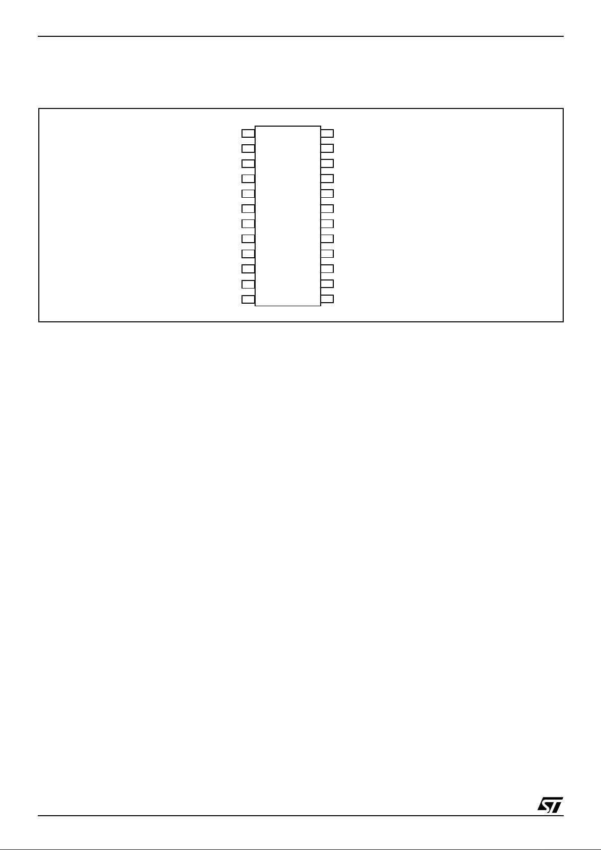
ST7SCR
6/102
PIN DESCRIPTION (Cont’d)
Figure 3. 24-Pin SO Package Pinout
14
13
11
12
15
16
17
18
LED0
DM
DP
USBVcc
OSCIN
OSCOUT
V
PP
1
2
3
4
5
6
7
8
9
10
DIODE
CRDCLK
CRDRST
CRDVCC
PA6
CRDIO
19
20
C8
CRDDET
ICCDATA/WAKUP2/PA0
V
DDA
C4
GNDA
ICCCLK/WAKUP2/PA1
NC
GND
21
22
23
24
V
DD
SELF
1
Page 7

ST7SCR
7/102
PIN DESCRIPTION (Cont’d)
Legend / Abbreviations:
Type: I = input, O = output, S = supply
In/Output level: C
T
= CMOS 0.3VDD/0.7VDD with
input trigger
Output level: HS = 10mA high sink (on N-buffer
only)
Port and control configuration:
– Input:float = floating, wpu = weak pull-up, int = in-
terrupt, ana = analog
– Output : OD = open drain, PP = push-pull
Refer to “I/O PORTS” on page 30 for more det ails
on the software configuration of the I/O ports.
Table 1. Pin Description
Pin n°
Pin Name
Type
Level
V
CARD
supplied
Port / Control
Main
Function
(after reset)
Alternate Function
TQFP64
SO24
Input
Output
Input Output
wpu
int
OD
PP
1 5 CRDRST O CTX X Smartcard Reset
2 NC Not Connected
3 6 CRDCLK O C
T
X X Smartcard Clock
4 NC Not Connected
57C4 O C
T
X X Smartcard C4
6 8 CRDIO I/O C
T
X X X Smartcard I/O
79C8 O C
T
X X Smartcard C8
8 3 GND S Ground
9 PB0 O C
T
X X Port B0
1)
10 PB1 O C
T
X X Port B1
1)
11 PB2 O C
T
X X Port B2
1)
12 PB3 O C
T
X X Port B3
1)
13 PB4 O C
T
X X Port B4
1)
14 PB5 O C
T
X X Port B5
1)
15 PB6 O C
T
X X Port B6
1)
16 PB7 O C
T
X X Port B7
1)
17 10 CRDDET I C
T
X Smartcard Detection
18 VDD S Power Supply voltage 4V-5.5V
19 11
PA0/WAKUP2/
ICCDATA
I/O C
T
X X X X Port A0
Interrupt, In-Circuit Communication
Data Input
20 12
PA1/WAKUP2/
ICCCLK
I/O C
T
X X X X Port A1
Interrupt, In-Circuit Communication
Clock Input
21 PA2/WAKUP2 I/O C
T
X X X X Port A2
1)
Interrupt
22 PA3/WAKUP2 I/O C
T
X X X X Port A3
1)
Interrupt
23 PD0 O C
T
X X Port D0
1)
24 PD1 O C
T
X X Port D1
1)
25 PD2 O C
T
X X Port D2
1)
1
Page 8
ST7SCR
8/102
26 PD3 O C
T
X X Port D3
1)
27 PD4 O C
T
X X Port D4
1)
28 PD5 O C
T
X X Port D5
1)
29 PD6 O C
T
X X Port D6
1)
30 PD7 O C
T
X X Port D7
1)
31 14 OSCIN C
T
Input/Output Oscillator pins. These pins connect a
4MHz parallel-resonant crystal, or an external source
to the on-chip oscillator.
32 15 OSCOUT C
T
33 VDD S Power Supply voltage 4V-5.5V
34 GND S Ground
35 PC0/WAKUP1 I C
T
X X PC0
1)
External interrupt
36 PC1/WAKUP1 I C
T
X X PC1
1)
External interrupt
37 PC2/WAKUP1 I C
T
X X PC2
1)
External interrupt
38 PC3/WAKUP1 I C
T
X X PC3
1)
External interrupt
39 PC4/WAKUP1 I C
T
X X PC4
1)
External interrupt
40 PC5/WAKUP1 I C
T
X X PC5
1)
External interrupt
41 PC6/WAKUP1 I C
T
X X PC6
1)
External interrupt
42 PC7/WAKUP1 I C
T
X X PC7
1)
External interrupt
43 16 V
PP
S
Flash programming voltage. Must be held low in normal operating mode.
44 17 PA6 I C
T
PA6
45 18 LED0 O HS X Constant Current Output
46 19 DM I/O C
T
USB Data Minus line
47 20 DP I/O C
T
USB Data Plus line
48 NC Not Connected
49 21 USBVCC O C
T
3.3 V Output for USB
50 22 V
DDA
S power Supply voltage 4V-5.5V
51 23 V
DD
S power Supply voltage 4V-5.5V
52 LED1 O HS X Constant Current Output
53 LED2 O HS X Constant Current Output
54 LED3 O HS X Constant Current Output
55 NC Not Connected
56 NC Not Connected
57 PA4 I/O C
T
X X X X Port A4
Pin n°
Pin Name
Type
Level
V
CARD
supplied
Port / Control
Main
Function
(after reset)
Alternate Function
TQFP64
SO24
Input
Output
Input Output
wpu
int
OD
PP
1
Page 9
ST7SCR
9/102
Note 1 : Keyboard interface
58 PA5 I/O C
T
X X X X Port A5
59 24 SELF2 O C
T
An External inductance must be connected to these
pins for the step up converter (refer to Figure 4 to
choose the right capacitance)
60 24 SELF1 O C
T
61 1 DIODE S C
T
An External diode must be connected to this pin for
the step up converter (refer to Figure 4 to choose the
right component)
62 2 GNDA S
Ground
63 3 GND S
64 4 CDRVCC O C
T
X Smartcard Supply pin
Pin n°
Pin Name
Type
Level
V
CARD
supplied
Port / Control
Main
Function
(after reset)
Alternate Function
TQFP64
SO24
Input
Output
Input Output
wpu
int
OD
PP
Page 10
ST7SCR
10/102
PIN DESCRIPTION (Cont’d)
Figure 4. Smartcard Interface Reference A pplication
Note 1: Refer to Section 6 on page 20.
LED0
DM
DP
USBVcc
OSCIN
OSCOUT
V
PP
DIODE
CRDCLK
CRDRST
CRDVCC
PA6
CRDIO
C8
CRDDET
PA0
V
DDA
C4
GNDA
PA1
NC
GND
V
DD
SELF
V
DD
C
L1
C
L2
C7
C8
C9
V
DD
L1
C5
D1
R
LED
C4
VBUS
D-
D+
GND
SHIELD
C2C1 C3
C6
V
DD
V
DD
D+
D-
Mandatory values for the external components :
C2 : 4.7 µF,ESR 0. 5 Ohm
L1 : 10 µH, 2 Ohm
C7 : 4.7 µF,ESR 0.5 Ohm
C5 : 1 nF
Crystal 4.0 MHz, Impedance m ax100 Ohm
Cl1 , C l2
1)
D1: BAT42 SHOTTKY
C6 : 10 0 nF
C8 : 470 pF
C9 :
100 pF
C1 : 100nF
C3 : 1 µF
C4 : 4.7 µF
R : 1.5kOhm
1
Page 11
ST7SCR
11/102
3 REGISTER & MEMORY MAP
As sho wn i n Figure 5, the MCU is capable of ad-
dressing 64K bytes of memories and I/O registers.
The available memory locations consist of 40
bytes of register locations, up to 512 bytes of RAM
and up to 16K bytes of user program memory. The
RAM space includes u p to 128 by t es fo r the stack
from 0100h to 017Fh.
The highest address bytes contain the user re set
and interrupt vectors.
IMPORTANT: Memory locations noted “Reserved” must ne ver be accessed. Ac cessing a reserved area can have unpredictable effects on the
device.
Figure 5. Me m ory M a p
0000h
Interrupt & Reset Vectors
HW Registers
0040h
003Fh
(see Table 2)
FFDFh
FFE0h
FFFFh
(see Table 7)
C000h
033Fh
Program Memory
RAM
USB RAM
(16K Bytes)
Short Addressing
Stack (128 Bytes)
0100h
0180h
023Fh
0040h
00FFh
017Fh
16-bit Addressing RAM
RAM (192 Bytes)
( 192 Bytes)
023Fh
0240h
256 Bytes
(512 Bytes)
Unused
1
Page 12

ST7SCR
12/102
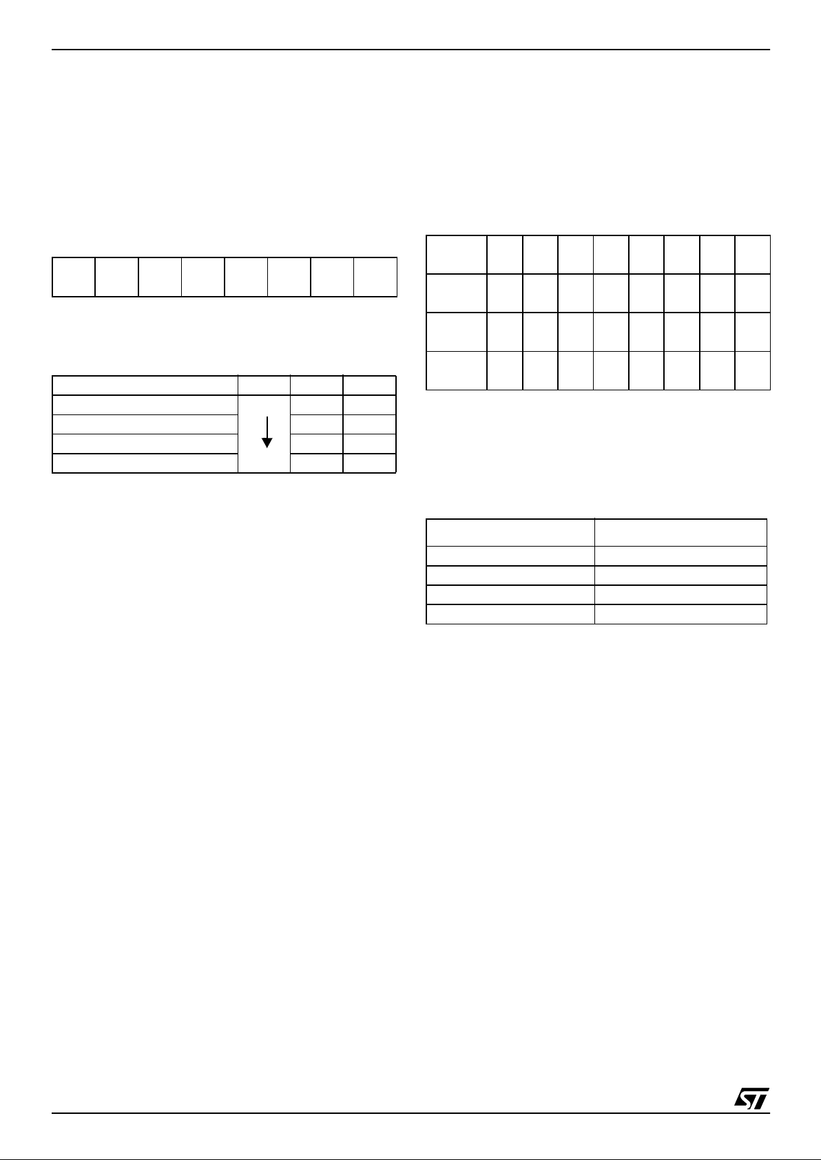
Table 2. Hardware Regist er Memo ry Ma p
Address Block
Register
Label
Register
name
Reset Status Remarks
0000h
0001h
0002h
0003h
0004h
0005h
0006h
0007h
0008h
0009h
000Ah
000Bh
000Ch
000Dh
CRD
CRDCR
CRDSR
CRDCCR
CRDETU1
CRDETU0
CRDGT1
CRDGT0
CRDWT2
CRDWT1
CRDWT0
CRDIER
CRDIPR
CRDTXB
CRDRXB
Smartcard Interface Control Register
Smartcard Interface Status Register
Smartcard Contact Control Register
Smartcard Elementary Time Unit 1
Smartcard Elementary Time Unit 0
Smartcard Guard time 1
Smartcard Guard time 0
Smartcard Character Waiting Time 2
Smartcard Character Waiting Time 1
Smartcard Character Waiting Time 0
Smartcard Interrupt Enable Register
Smartcard Interrupt Pending Register
Smartcard Transmit Buffer Register
Smartcard Receive Buffer Register
00h
80h
xxh
01h
74h
00h
0Ch
00h
25h
80h
00h
00h
00h
00h
R/W
R/W
R/W
R/W
R/W
R/W
R/W
R/W
R/W
R/W
R/W
R
R/W
R
000Eh Watchdog WDGCR Watchdog Control Register 00h R/W
0011h
0012h
0013h
0014h
Port A
PADR
PADDR
PAOR
PAPUCR
Port A Data Register
Port A Data Direction Register
Option Register
Pull up Control Register
00h
00h
00h
00h
R/W
R/W
R/W
R/W
0015h
0016h
0017h
Port B
PBDR
PBOR
PBPUCR
Port B Data Register
Option Register
Pull up Control Register
00h
00h
00h
R/W
R/W
R/W
0018h Port C PCDR Port C Data Register 00h R/W
0019h
001Ah
001Bh
Port D
PDDR
PDOR
PDPUCR
Port D Data Register
Option Register
Pull up Control Register
00h
00h
00h
R/W
R/W
R/W
001Ch
001Dh
001Eh
001Fh
MISC
MISCR1
MISCR2
MISCR3
MISCR4
Miscellaneous Register 1
Miscellaneous Register 2
Miscellaneous Register 3
Miscellaneous Register 4
00h
00h
00h
00h
R/W
R/W
R/W
R/W
1
Page 13

ST7SCR
13/102
0020h
0021h
0022h
0023h
0024h
0025h
0026h
0027h
0028h
0029h
002Ah
002Bh
002Ch
002Dh
002Eh
002Fh
0030h
0031h
0032h
0033h
0034h
USB
USBISTR
USBIMR
USBCTLR
DADDR
USBSR
EPOR
CNT0RXR
CNT0TXR
EP1TXR
CNT1TXR
EP2RXR
CNT2RXR
EP2TXR
CNT2TXR
EP3TXR
CNT3TXR
EP4TXR
CNT4TXR
EP5TXR
CNT5TXR
ERRSR
USB Interrupt Status Register
USB Interrupt Mask Register
USB Control Register
Device Address Register
USB Status Register
Endpoint 0 Register
EP 0 ReceptionCounter Register
EP 0 Transmission Counter Register
EP 1 Transmission Register
EP 1 Transmission Counter Register
EP 2 Reception Register
EP 2 Reception Counter Register
EP 2 Transmission Register
EP 2 Transmission Counter Register
EP 3 Transmission Register
EP 3 Transmission Counter Register
EP 4 Transmission Register
EP 4 Transmission Counter Register
EP 5 Transmission Register
EP 5 Transmission Counter Register
Error Status Register
00h
00h
06h
00h
00h
0xh
00h
00h
00h
00h
00h
0xh
00h
00h
00h
00h
00h
00h
00h
00h
00h
R/W
R/W
R/W
R/W
R/W
R/W
R/W
R/W
R/W
R/W
R/W
R/W
R/W
R/W
R/W
R/W
R/W
R/W
R/W
R/W
R/W
0035h
0036h
TBU
TBUCV
TBUCSR
Timer counter value
Timer control status
00h
00h
R/W
R/W
0037h
0038h
0039h
003Ah
ITC
ITSPR0
ITSPR1
ITSPR2
ITSPR3
Interrupt Software Priority Register 0
Interrupt Software Priority Register 1
Interrupt Software Priority Register 2
Interrupt Software Priority Register 3
FFh
FFh
FFh
FFh
R/W
R/W
R/W
R/W
003Bh Flash FCSR Flash Control Status Register 00h R/W
003Eh LED_CTRL LED Control Register 00h R/W
Address Block
Register
Label
Register
name
Reset Status Remarks
1
Page 14
ST7SCR
14/102
4 FLASH PROGRAM MEMORY
4.1 Introduction
The ST7 dual voltage High Density Flash (HDFlash) is a non-volatile memory that can be electrically erased as a single block or by individual sectors and programmed on a Byte-by-Byte basis using an external V
PP
supply.
The HDFlash devices can be programmed and
erased off-board (plugge d in a programm ing tool)
or on-board using ICP (In-Circuit Programming) or
IAP (In-Application Programming).
The array matrix organ isation allows each sector
to be erased and reprogramm ed without affecting
other sectors.
4.2 Main Features
■ Three Flash programming modes :
– Insertion in a programming tool. In this m ode,
all sectors including option bytes can be programmed or erased.
– ICP (In-Circuit Programming). In this mode, all
sectors including option bytes can be programmed or erased without removing the device from the application board.
– IAP (In-Application Programming) In this
mode, all sectors except Sector 0, can be programmed or erased without removing the device from the application board a nd wh ile the
application is running.
■ ICT (In-Circuit Testing) for downloading and
executing user application test patterns in RAM
■ Read-out protection against piracy
■ Register Access Security System (RASS) to
prevent accidental programming or erasing
4. 3 S truct u re
The Flash memory is organised in sectors and can
be used for both code and data storage.
Depending on the overall FLASH memory size i n
the microcontroller device, there are up to three
user sectors (see Table 3). Each of these sec tors
can be erased independently to avoid unnecessary erasing of the whole Flash memory when only
a partial erasing is required.
The first two sectors have a fixed siz e of 4 Kby tes
(see Figure 6). They are mapped in the upper part
of the ST7 addressing space so t he reset and interrupt vectors are located in Sector 0 (F000hFFFFh).
Table 3. Sectors available in FLASH devices
Figure 6. Memory map and sector address
Flash Memory Size
(bytes)
Available Sectors
4K Sector 0
8K Sectors 0,1
> 8K Sectors 0,1, 2
4 Kbytes
4 Kbytes
SECTOR 1
SECTOR 0
SECTOR 2
16K USER FLASH MEMORY SIZE
FFFFh
F000h
EFFFh
E000h
DFFFh
C000h
8Kbytes
ex.: user program
ex.: user data
ex.: user system library
+ IAP BootLoader
+ libra ry
1
Page 15
ST7SCR
15/102
FLASH PROGRAM MEMORY (Cont’d)
4.4 ICP (In-Circuit Programming)
To perform ICP the microcontroller must be
switched to ICC (In-Circuit Communication) mode
by an external controller or programming tool.
Depending on the ICP code dow nloaded in RAM,
Flash memory programming can be fully customized (number of bytes to prog ram, program locations, or selection serial communication interface
for downloading).
When using an STMicroelectronics or third-party
programming tool that supp orts ICP and the specific microcontroller device, the user needs only to
implement the ICP hardware interface on the application board (see Figure 7). For more details on
the pin locations, refer to the device pinout description.
ICP needs six signals to be connec ted to the programming tool. These signals are:
–V
SS
: device power supply ground
–V
DD
: for re s e t by LV D
– OSCIN: to force the clock during power-up
– ICCCLK: ICC output serial clock pin
– ICCDATA: ICC input serial data pin
–V
PP
: ICC mode selection and programming
voltage.
If ICCCLK or ICCDATA are used for other purposes in the application, a serial resistor has to be implemented to avoid a conflict in case one of the
other devices forces the signal level.
Note: To develop a c usto m program mi ng tool, refer to the ST7 FLASH Programmin g and I CC Re ference Manual which gives full details on the ICC
protocol hardware and software.
4.5 IAP (In-Application Programming)
This mode uses a BootLoader program previously
stored in Sector 0 by the user (in ICP mode or by
plugging the device in a programming tool).
This mode is fully controlled by user software. This
allows it to be adapted to the user application, (user-defined strategy for entering programming
mode, choice of communications protocol us ed to
fetch the data to be stored, etc.). For example, it is
possible to download code from the USB interface
and program it in the Flash. IAP mode can be used
to program any of the Flash sectors except Sector
0, which is write/erase protected to allow recovery
in case errors occur during the programming operation.
Figure 7. Typical ICP Interface
ICP PROGRAMMING TOOL CONNECTOR
10k
Ω
C
L2
C
L1
ICCDATA
ICCCLK
V
SS
V
PP
OSCIN
OSCOUT
ST7
HE10 CONNECTOR TYPE
T
OT
HE A
PP
L
ICA
TION
V
DD
4.7k
Ω
APPLICATION BOARD
1
246810
975 3
PROGRAMMING TOOL
ICC CONNECTOR
ICC C a ble
1
Page 16

ST7SCR
16/102
FLASH PROGRAM MEMORY (Cont’d)
Note: If the ICCCLK or ICCDATA pins are only
used as outputs in the application, no signal isolation is necessary. As soon as the Programming
Tool is plugged to the boa rd, even if an ICC session is not in progress, the ICCCLK and ICCDATA
pins are not available for the application. If they
are used as inputs by the application, isolation
such as a serial resistor has to implemented in
case another device forces the signal. Refer to the
Programming Tool documentation for recommended resistor values.
4.6 Program Memo ry Read-out P rotection
The read-out protection is enabled through an option bit.
For Flash devices, when this option is selected,
the program and data stored in the F lash m em ory
are protected ag ainst rea d-out piracy (i ncluding a
re-write protection). When this protection is removed by reprogramming the Option Byte, the en-
tire Flash program memory is first automatically
erased.
Refer to the Option By te description for more details.
4.6.1 Register Description
FLASH CONTROL/STATUS REGISTER (FCSR)
Read/Write
Reset Value: 0000 0000 (00h)
This register is reserved for use by Programming
Tool software. It controls the FLASH programming
and erasing operations. For details on customizing
FLASH programming methods and In-Circuit Testing, refer to the ST7 FLASH Programming and
ICC Reference Manual.
70
00000000
1
Page 17
ST7SCR
17/102
5 CENTRAL PRO CESSING UNIT
5.1 INTRODUCTION
This CPU has a full 8-bit architecture and contains
six internal registers allowing efficient 8-bit data
manipulation.
5.2 MAIN FEATURES
■ Enable executing 63 basic instructions
■ Fast 8-bit by 8-bit multiply
■ 17 main addressing modes (with indirect
addressing mode)
■ Two 8-bit index registers
■ 16-bit stack pointer
■ Low power HALT and WAIT modes
■ Priority maskable hardware interrupts
■ Non-maskable software/hardware interrupts
5.3 CPU REGISTERS
The 6 CPU registers shown in Figure 8 are not
present in the memory mapping and are accessed
by spec ifi c ins t ru c tio n s .
Accumulator (A)
The Accumulator is an 8-bit general purpose register used to hold operands and the res ults of the
arithmetic and logic calculations and to manipulate
data.
Index Registers (X and Y)
These 8-bit registers are used to create effective
addresses or as tempo rary storage areas f or data
manipulation. (The Cross -Assembler generates a
precede instruction (PRE) to indicate that the following instruction refers to the Y register.)
The Y register is not affected by the interrupt automatic procedures.
Program Counter (PC)
The program counter is a 16-bit register containing
the address of the next instruction to be executed
by the CPU. It is made of two 8-bit registers PCL
(Program Counter Low which is the LSB) and PCH
(Program Counter High which is the MSB).
Figure 8. CPU Registers
ACCUMULA TOR
X INDEX REGISTER
Y INDEX REGISTER
STACK POINTER
CONDITION CODE REGISTER
PROGRAM COUNTER
70
1C1I1HI0NZ
RESET VALUE = RESET VECTOR @ FFFEh-FFFFh
70
70
70
0
7
15 8
PCH
PCL
15
8
70
RESET VALUE = STACK HIGHER ADDRESS
RESET VALUE =
1X11X1XX
RESET VALUE = XXh
RESET VALUE = XXh
RESET VALUE = XXh
X = Undefined Value
1
Page 18
ST7SCR
18/102
CENTRAL PROC ESSING UNIT (Cont’d)
Condition Code Reg ister (CC)
Read/Write
Reset Value: 111x1xxx
The 8-bit Condition Code regist er contains the i nterrupt masks and four flags representative of the
result of the instruction just executed. This register
can also be handled by the PUSH and POP instructions.
These bits can be individually tested and/or controlled by specific instructions.
Arithmetic Management Bits
Bit 4 = H
Half carry
.
This bit is set by hardware when a carry occurs between bits 3 and 4 of t he ALU during an ADD or
ADC instructions. It is reset by hardware during
the same instructio n s.
0: No half carry has occurred.
1: A half carry has occurred.
This bit is tested using the JRH or JRNH in struction. The H bit is useful in BCD arithmetic subroutine s .
Bit 2 = N
Negative
.
This bit is set and cleared by hardware. It is representative of the result sign of the last arithmetic,
logical or data manipulation. I t’s a copy of the result 7
th
bit.
0: The result of the last operation is positive or null.
1: The result of the last operation is negative
(i.e. the most significant bit is a logic 1).
This bit is accesse d by the JRMI and JRPL instructions.
Bit 1 = Z
Zero
.
This bit is set and cleared by hardware. This bit indicates that the result of the last arithme tic, logical
or data manipulation is zero.
0: The result of the last operation is dif ferent from
zero.
1: The result of the last operation is zero.
This bit is accessed by the JREQ and JRNE test
instructions.
Bit 0 = C
Carry/borrow.
This bit is set and cleared b y hardware and software. It indicates an overflow or an un derflow has
occurred during the last arithmetic operation.
0: No overflow or underflow has occurred.
1: An overflow or underflow has occurred.
This bit is driven by th e SCF and RCF instructions
and tested by the JRC and JRNC instructions. It i s
also affected by the “bit test and branch”, shift and
rotate instructions.
Interrupt Managem ent B i ts
Bit 5,3 = I1, I0
Interrupt
The combination of the I1 and I0 bits gives the current interrupt software priority.
These two bits are set/cleared by hardware when
entering in interrupt. The loaded value is given by
the corresponding bits in the interrupt software priority registers (IxSPR). They can be also set/
cleared by software with the RIM, SIM, IRET,
HALT, WFI and PUSH/POP instructions.
See the interrupt management chapter for more
details.
70
11I1HI0NZ
C
Interrupt Software Priorit y I1 I0
Level 0 (main) 1 0
Level 1 0 1
Level 2 0 0
Level 3 (= interrupt disable) 1 1
1
Page 19
ST7SCR
19/102
CENTRAL PROC ESSING UNIT (Cont’d)
Stack Poi nter (SP)
Read/Write
Reset Value: 017Fh
The Stack Pointer is a 16-bit register which is always pointing to the next free location in the stack.
It is then decremented after data has been pushed
onto the stack and incremented before data is
popped from the stack (see Figure 9).
Since the stack is 256 bytes deep, the 8 most significant bits are forced by hard ware. Following a n
MCU Reset, or after a Reset Stack Pointer instruction (RSP), the Stack Pointer contains its reset value (the SP7 to SP0 bits are set) which is the stack
higher address.
The least significant byte of the Stack Pointer
(called S) can be directly accessed by a LD instruction.
Note: When the lower limit is exceeded, the Stack
Pointer wraps around to the stack upper limit, without indicating the stack overflow. The previously
stored information is then o verwritten and therefore lost. The stack also wraps in case of an underflow.
The stack is used to sav e the return address during a subroutine call and the CPU context during
an interrupt. The user may also directly manipulate
the stack by means of the PUSH and POP instructions. In the case of an interrupt, the PCL is stored
at the first location po inted t o by t he SP. Th en t he
other registers are stored in the next locations as
shown in Figure 9
– When an interrupt is received, the SP is decre-
mented and the context is pushed on the stack.
– On return from interrupt, the SP is incremented
and the context is popped from the stack.
A subroutine call occupies two locations and an interrupt five locat ion s i n the stack ar ea.
Figure 9. Stack Manipulation Example
15 8
00000001
70
SP7 SP6 SP5 SP4 SP3 SP2 SP1
SP0
PCH
PCL
SP
PCH
PCL
SP
PCL
PCH
X
A
CC
PCH
PCL
SP
PCL
PCH
X
A
CC
PCH
PCL
SP
PCL
PCH
X
A
CC
PCH
PCL
SP
SP
Y
CALL
Subroutine
Interrupt
Event
PUSH Y POP Y IRET
RET
or RSP
@ 017Fh
@ 0100h
Stack Higher Address = 017Fh
Stack Lower Address =
0100h
1
Page 20
ST7SCR
20/102
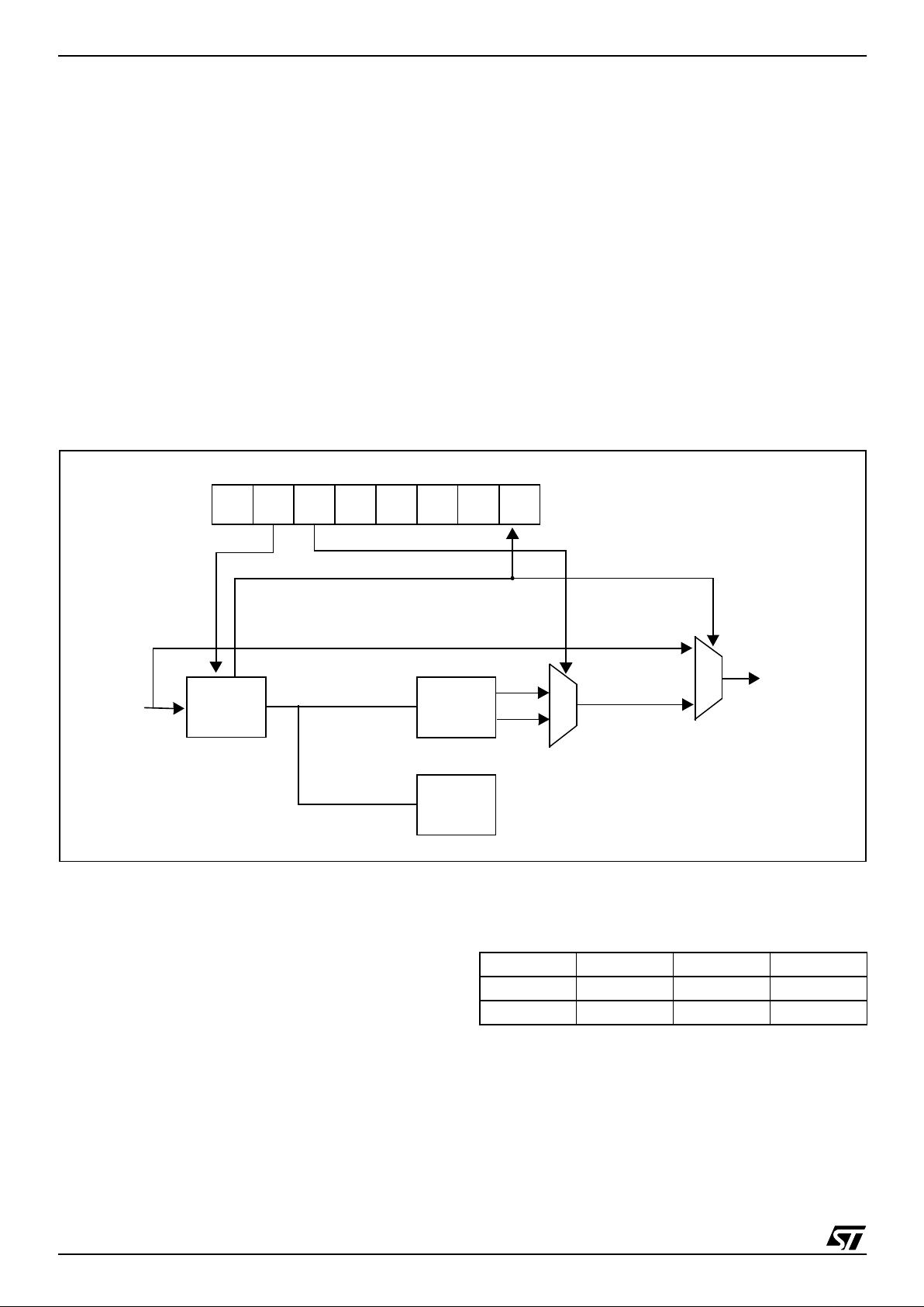
6 SUPPLY, RESET AND CLOCK MANAGEMENT
6.1 CLOCK SYSTEM
6.1.1 General Description
The MCU accepts either a 4MHz crystal or an external clock signal to drive the internal oscillator.
The internal clock (f
CPU
) is derived from the inter-
nal oscillat o r freq uency (f
OSC
), which is 4 Mhz .
After reset, the internal clock (f
CPU
) is provided by
the internal oscillator (4Mhz frequency).
To activate the 48-MHz clock for the USB inter-
face, the user mus t turn on the PLL by setting the
PLL_ON bit in the MISCR4 register. When the PLL
is locked, the LOCK bit is set by hardware.
The user can then select an internal frequency
(f
CPU
) of either 4 MHz or 8MHz by programming
the CLK_SEL bit in t he MISCR4 register (refer to
MISCELLANEOUS REGISTERS section on page
37).
The PLL provides a signal with a duty cycle of 50
%.
The internal clock signal (f
CPU
) is also routed to
the on-chip peripherals. The CPU clock signal
consists of a square wave with a duty cycle of
50%.
Figure 10. Clock, Reset and Supply Block Diagram
The internal oscillat or is designed to operate with
an AT-cut parallel resonant quartz in the frequency range specified for f
osc
. The circuit shown in
Figure 12 is recommend ed when using a crystal,
and Table 4 lists the recommended capacitance.
The crystal and associated components should be
mounted as close as p ossible to the input pins i n
order to minimize output distortion and start-up
stabilisation time. The LOCK bit in the MISCR4
register can also be used to generat e the f
CPU
di-
rectly from f
OSC
if the PLL and the US B interface
are not active.
Table 4. Recommended Values for 4 MHz
Crystal Resonator
Note: R
SMAX
is the equivalent serial resistor of the
crystal (see crystal specification).
PLL_
MISCR4
ON
-
-
----
LOCK
4 Mhz
INTERNAL
8 Mhz
CLOCK (f
CPU
)
4 MHz
PLL
X 12
48 MHz
USB
48 MHz
DIV
(f
OSC
)
CLK_
SEL
R
SMAX
20
Ω
25
Ω
70
Ω
C
OSCIN
56pF 47pF 22pF
C
OSCOUT
56pF 47pF 22pF
1
Page 21
ST7SCR
21/102
CLOCK SYSTEM (Cont’d)
6.1.2 External Clock
An external clock may be applied to the OSCIN input with the OSCOUT pin not connected, as
shown on Figure 11.
Figure 11. .External Clock Source Connections
Figure 12. Crystal Resonator
OSCIN OSCOUT
EXTERNAL
CLOCK
NC
OSCIN OSCOUT
C
OSCIN
C
OSCOUT
1
Page 22
ST7SCR
22/102
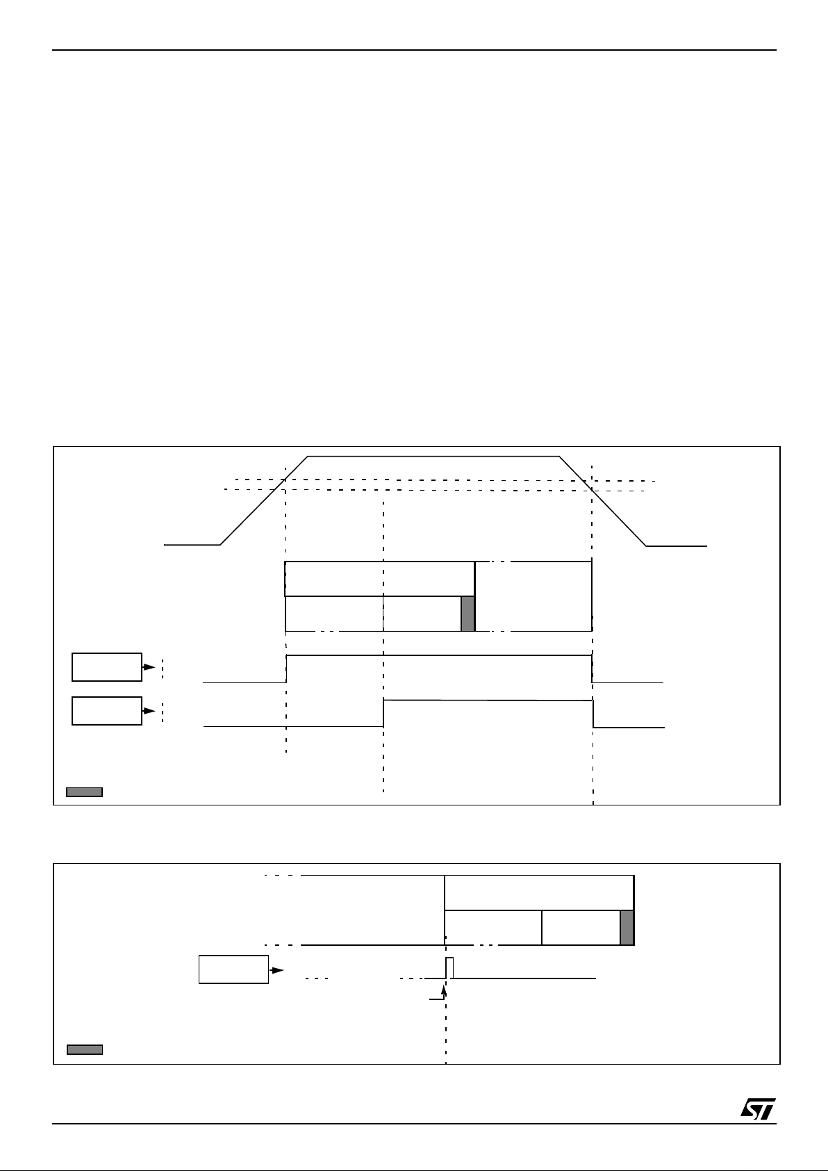
6.2 RESET SEQUENCE MANAGER (RSM)
6.2.1 Introd uc tion
The reset sequence manager has two reset sources:
■ Internal LVD reset (Low Voltage Detection)
which includes both a power-on and a voltage
drop reset
■ Internal watchdog reset generated by an
internal watchdog counter unde rflow as shown
in Figure 14.
6.2.2 Functional Description
The reset service routine vector is fixed at addresses FFFEh-FFFFh in the ST7 memory map.
The basic reset sequence consists of 3 phases as
shown in Figure 13:
■ A first delay of 30µs + 127 t
CPU
cycles during
which the internal reset is maintained.
■ A second delay of 512 t
CPU
cycles after the
internal reset is generated. It allows the
oscillator to stabilize and ens ures that recovery
has taken place from the Reset state.
■ Reset vector fe tch (duration: 2 clock cycles)
Low Voltage Detector
The low voltage detector gene rates a reset when
V
DD<VIT+
(rising edge) or VDD<V
IT-
(falling edge),
as shown in Figure 13.
The LVD filters spikes on V
DD
larger than t
g(VDD)
to
avoid para siti c rese ts. Se e “ SUP PLY AND RESET
CHARACTERISTICS” on page 79.
Figure 13. LVD RESET Sequence
Figure 14. Watchd og RESET Seque nce
DELAY 1
RUN
LVD
RESET
FETCH VECTOR (2 t
CPU
)
DELAY 2
LVD
RESET
INTERNAL
RESET
DELAY 1 = 30µs + 127 t
CPU
DELAY 2 = 512 t
CPU
V
DD
V
IT+
V
IT-
WATCHDOG
WATCHDOG UN DE RFL OW
RESET
FETCH VECTOR (2 t
CPU
)
DELAY 1
WATCHDOG
RESET
DELAY 2
DELAY 1 = 30µs + 127 t
CPU
DELAY 2 = 512 t
CPU
RUN
1
Page 23
ST7SCR
23/102
7 INTERRUP T S
7.1 INTRODUCTION
The ST7 enhanced interrupt management provides the following features:
■ Hardware interrupts
■ Software interrupt (TRAP)
■ Nested or concurrent interrupt management
with flexible interrupt priority and level
management:
– Up to 4 software programmable nesting levels
– Up to 16 interrupt vectors fixed by hardware
– 3 non maskable events: TLI, RESET, TRAP
This interrupt management is based on:
– Bit 5 and bit 3 of the CPU CC register (I1:0),
– Interrupt software priority registers (ISPRx),
– F ixed interrupt vecto r addresses locat ed at the
high addresses of the memory map (FFE0h to
FFFFh) sorted by hardware priority order.
This enhanced interrupt cont roller guarantees full
upward compatibility with the standard (not nested) ST7 interrupt controller.
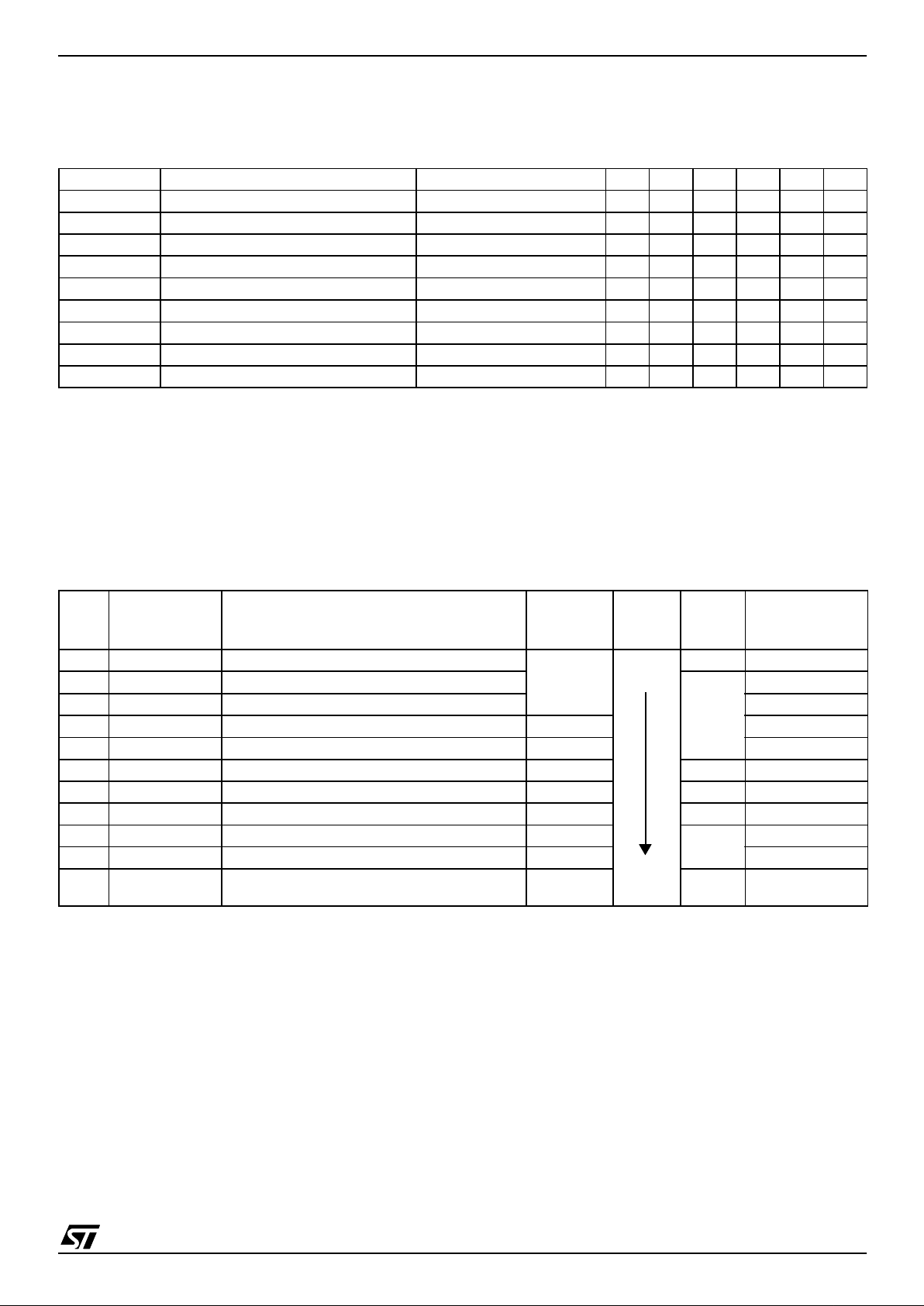
7.2 MASKI N G AND PRO C ESSING FLOW
The interrupt masking is managed by the I1 and I0
bits of the CC register and the ISPRx registers
which give the interrupt software priority level of
each interrupt vector (see Table 5 ). The processing flow is shown in Figure 15 .
When an interrupt request has to be serviced:
– Normal processing is suspended at the end of
the current instruction execution.
– The PC, X, A and CC registers are saved onto
the stack.
– I1 and I0 bits of CC register are set according to
the corresponding values in the ISPRx registers
of the serviced interrupt vector.
– The PC is then loaded with the interrupt vector of
the interrupt to service and the first instruction of
the interrupt service routine is fetched (refer to
“Interrupt Mapping” table for vector addresses).
The interrupt service routine should end with the
IRET instruction which c auses the contents of the
saved registers to be recovered from the stack.
Note: As a cons equence of the IRET instruction,
the I1 and I0 bits will be restored from the stack
and the program in the previous level will resume.
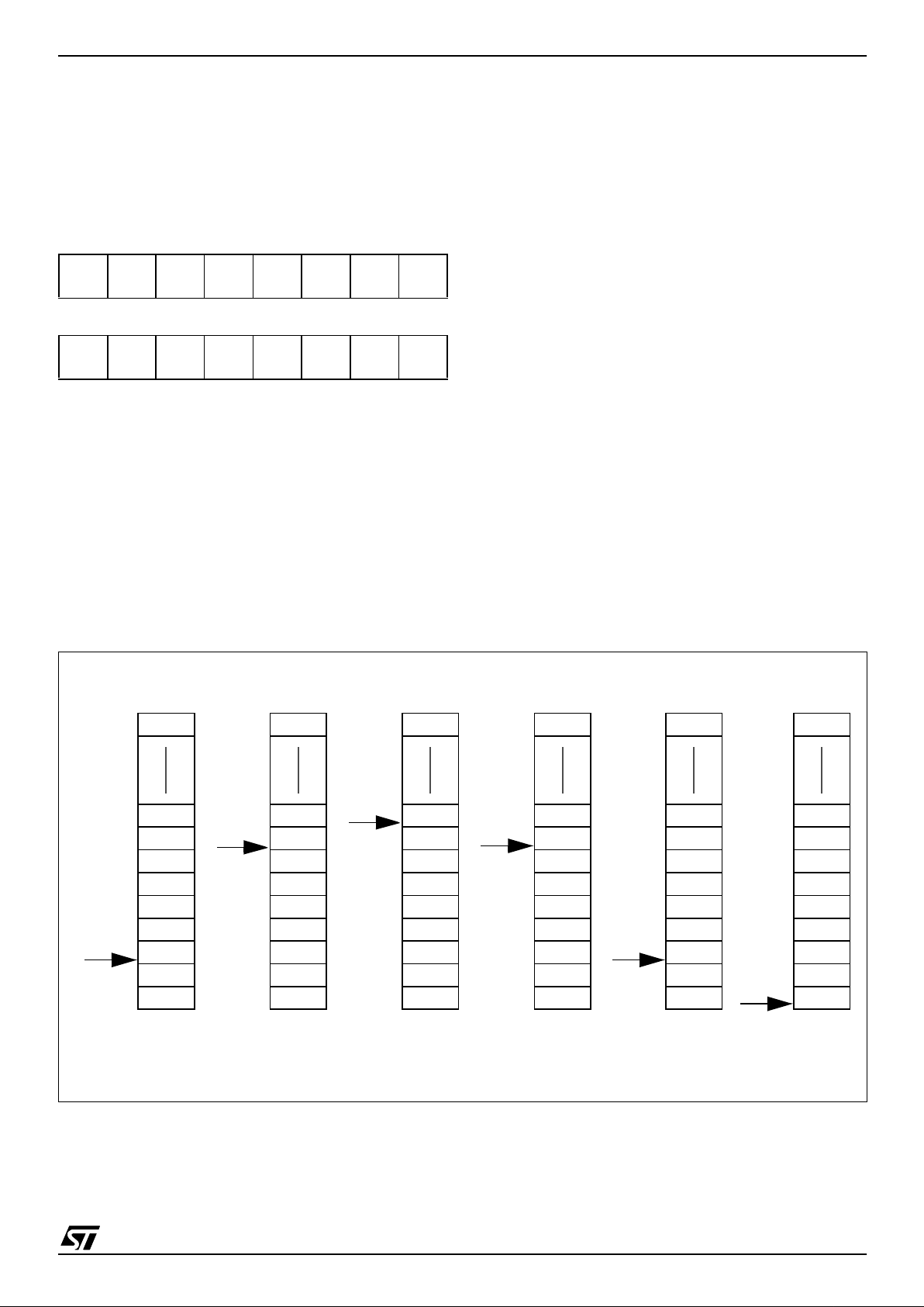
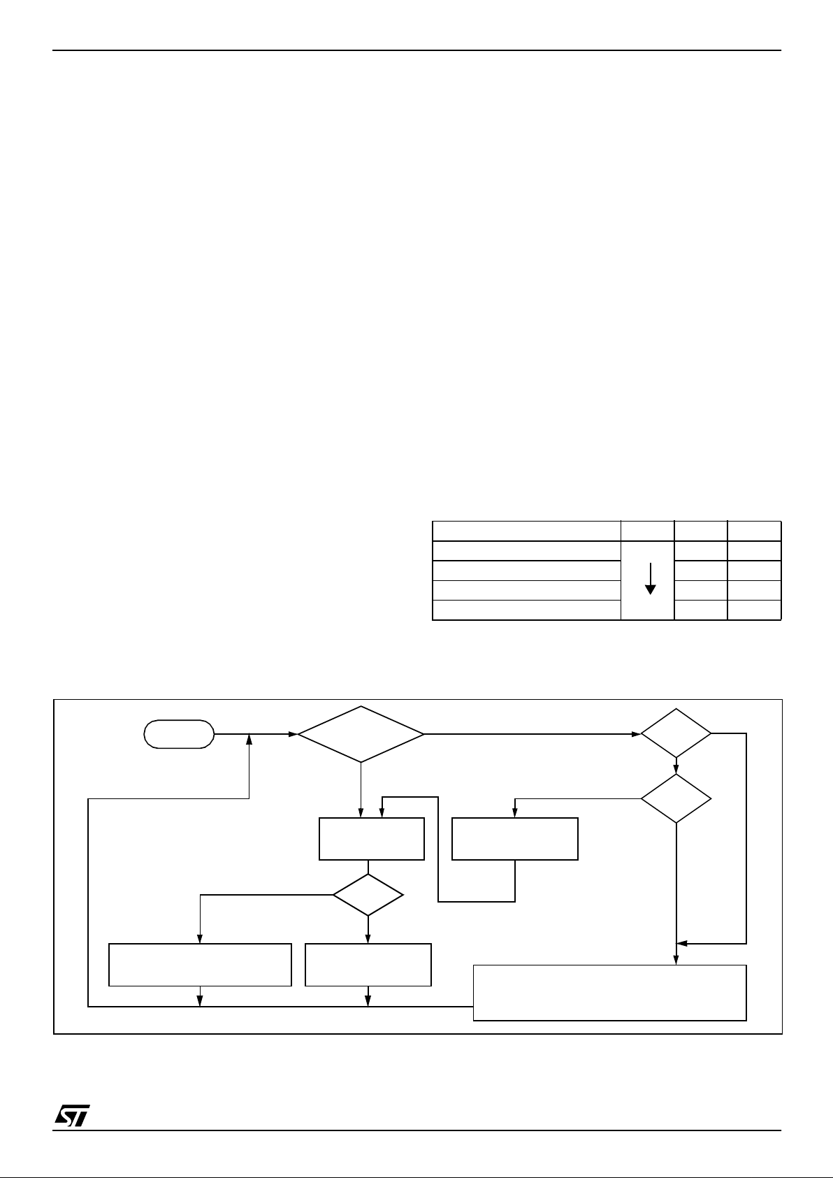
Table 5. Interrupt Software Priority Levels
Figure 15. Int errupt Processing Flow c hart
Interrupt software priority Le vel I1 I0
Level 0 (main) Low
High
10
Level 1 0 1
Level 2 0 0
Level 3 (= interrupt disable) 1 1
“IRET”
RESTORE PC, X, A, CC
STACK PC, X, A, CC
LOAD I1:0 FROM INTERR UPT SW REG.
FETCH NEX T
RESET
TLI
PENDING
INSTRUCTION
I1:0
FROM STACK
LOAD PC FROM INTERRUPT VECTOR
Y
N
Y
N
Y
N
Interrupt has the same or a
lower software priority
THE INTERRUPT
STAYS PENDING
than c u rrent one
Interrupt has a higher
softwarepr iority
than current one
EXECUTE
INSTRUCTION
INTERRUPT
1
Page 24
ST7SCR
24/102
INTERRUPTS (Cont’d)
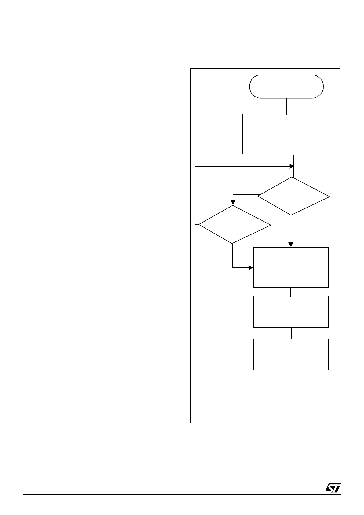
Servicing Pending In te rrup t s
As several interrupts can b e pen ding at the s ame
time, the interrupt to be taken into account is determined by the following two-step process:
– the highest software priority interrupt is serviced,
– i f several interrupts have the same software pri-
ority then the interrupt with the highest hardware
priority is serviced first.
Figure 16 describes this decision process.
Figure 16. Priority Decision Process
When an interrupt request is not serviced immediately, it is latched and then processed when its
software priority combined with the hardware priority becomes the highest one.
Note 1: The hardware priority is exclusive while
the software one i s not. This allows the prev ious
process to succeed with only one interrupt.
Note 2: RESET, TRAP and TLI are non maskable
and they can be considered as havin g the highest
software priority in the decision process.
Different Interrupt Vector Sources
Two interrupt source types are managed by the
ST7 interrupt controller: the non-maskable type
(RESET, TLI, TRAP) and the maskable type (external or from internal peripherals).
Non-Maskable Sources
These sources are processed regardless of the
state of the I1 and I0 bits of the CC register (see
Figure 15). After stacking the PC, X, A and CC
registers (except for RESET), the corresponding
vector is loaded in the PC register and t he I1 and
I0 bits of the CC are set to disable interrupts (level
3). These sources allow the processor to exit
HALT mode.
■ TLI (Top Level Hardware Interrupt)
This hardware interrupt occurs when a specific
edge is detected on the dedicated TLI pin.
Caution: A TRAP instruction must not be used in a
TLI service routine.
■ TRAP (Non Maskable Software Interrupt)
This software interrupt is serviced when the TRAP
instruction is executed. It will be serviced according to the flowchart in Figure 15 as a TLI.
Caution: TRAP can be interrupted by a TLI.
■ RESET
The RESET source has the highe st priority in the
ST7. This means that the first current routine has
the highest software priority (level 3) and the highest hardware priority.
See the RESET chapter for more details.
Maskable Sources
Maskable interrup t vector sourc es can be servi ced
if the corresponding in terrupt is enabled and if its
own interrupt software priority (in ISPRx registers)
is higher than the one currently being serviced (I1
and I0 in CC register). If any of these two co nditions is false, the interrupt is la tched and thus remains pending.
■ External Interrupts
External interrupts allow the processor to exit from
HALT low power mode.
External interrupt sensitivity is software selectable
through the External Interrupt Control register
(EICR).
External interrupt triggered on edge will be latched
and the interrupt request automatically cleared
upon entering the interrupt service routine.
If several input pins of a group connected to the
same interrupt line are selected simultaneously,
these w ill be log i cally NANDed.
■ Peripheral Interrupts
Usually the peripheral interrupts cause the MCU to
exit from HALT mode except thos e mentioned in
the “Interrupt Mapping” table.
A peripheral interrupt occurs when a specific flag
is set in the peripheral status registers and if the
corresponding enable bit is set in the peripheral
control register.
The general sequence for clearing an interrupt is
based on an access to the status register followed
by a read or write to an associated register.
Note: The clearing sequence resets the internal
latch. A pending interrupt (i.e. waiting for being
serviced) will therefore be lost if the clear sequence is executed.
PENDING
SOFTWARE
Different
INTERRUPTS
Same
HIGHEST HARDWARE
PRIORITY SERVICED
PRIORITY
HIGHEST SOFTWARE
PRIORITY SERVICED
1
Page 25
ST7SCR
25/102
INTERRUPTS (Cont’d)
7.3 INTERRUPTS AND LOW POWER MODES
All interrupts allow the processor to exit the WAIT
low power mode. On the contrary, only external
and other specified interrupt s allow the processor
to exit from the HALT modes (see column “Exit
from HALT” in “Interrupt Mapping” table). When
several pending interrupts are present whi le exiting HALT mode, the first one serviced can only be
an interrupt with e xit from HALT mode c apability
and it is selected through the same decision proc ess shown in Figure 16.
Note: If an interrupt, that is not able to Exit from
HALT mode, is pending with the highest priority
when exiting HALT mode, this interrupt is serviced
after the first one serviced.
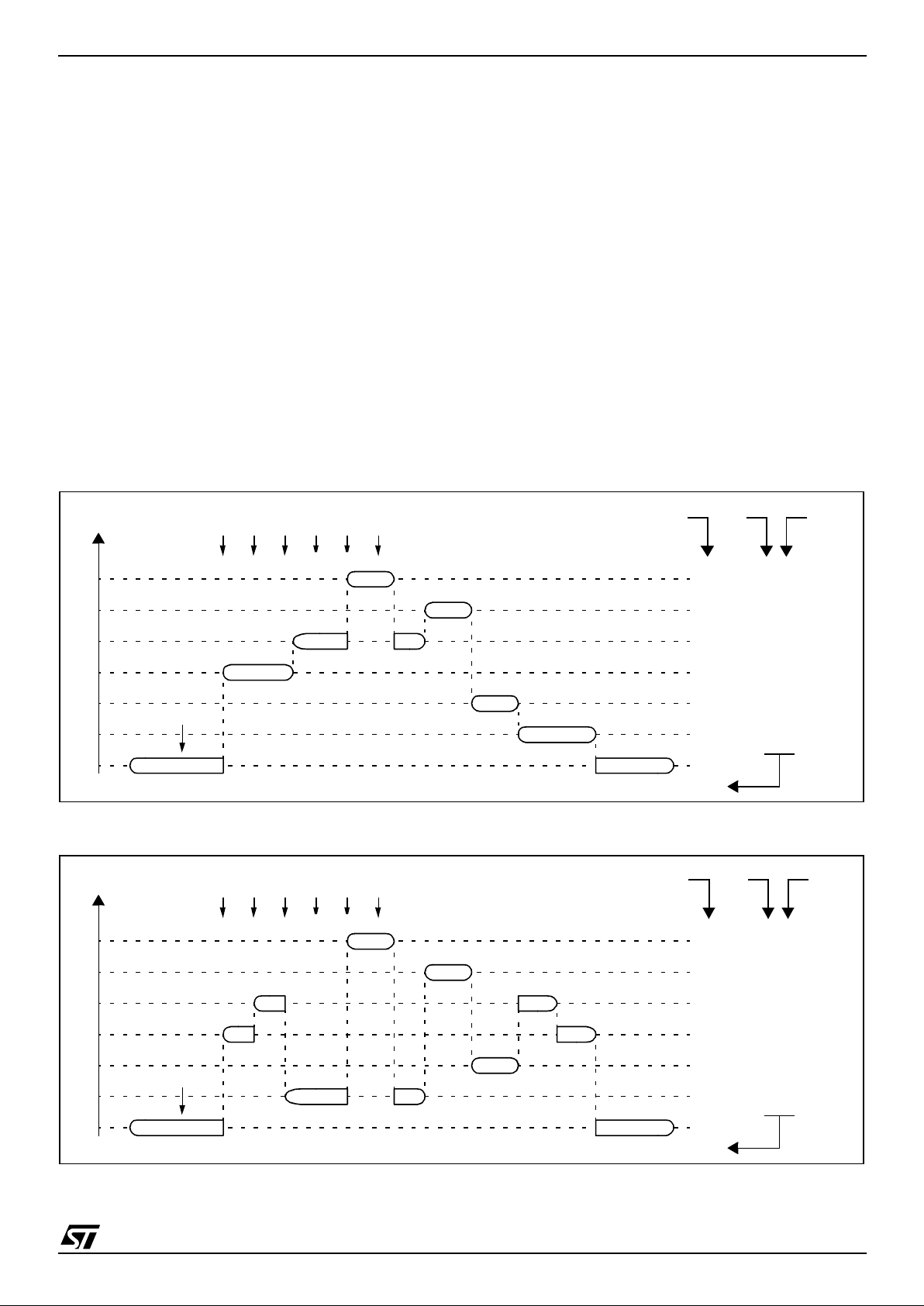
7.4 CONCURRENT & NESTED MANAGEMENT
The following Figure 17 and Figure 18 show two
different interrupt management modes. The first is
called concurrent mode and do es not allow an interrupt to be interrupted, unlike the nested mode in
Figure 18. The interrupt hardware priority is given
in this order from the l owes t to the hi ghest: M A IN,
IT4, IT3 , IT2, IT1, IT0, TLI. The software priority is
given for each interrupt.
Warning: A stack overflow may occur without notifying the software of the failure.
Figure 17. Concurrent Interrupt Managem ent
Figure 18. Nested Interrupt Management
MAIN
IT4
IT2
IT1
TLI
IT1
MAIN
IT0
I1
HARDWARE PRIORITY
SOFTWARE
3
3
3
3
3
3/0
3
11
11
11
11
11
11 / 10
11
RIM
IT2
IT1
IT4
TLI
IT3
IT0
IT3
I0
10
PRIORITY
LEVEL
USED STACK = 10 BYTES
MAIN
IT2
TLI
MAIN
IT0
IT2
IT1
IT4
TLI
IT3
IT0
HARDWARE PRIORITY
3
2
1
3
3
3/0
3
11
00
01
11
11
11
RIM
IT1
IT4
IT4
IT1
IT2
IT3
I1 I0
11 / 10
10
SOFTWARE
PRIORITY
LEVEL
USED STACK = 20 BYTES
1
Page 26
ST7SCR
26/102
INTERRUPTS (Cont’d)
7.5 INTERRUPT REGISTER DESCRIPTION
CPU CC REGISTER INTERRUPT BITS
Read/Write
Reset Value: 111x 1010 (xAh)
Bit 5, 3 = I1, I0
Soft w a re In te r r u p t Priority
These two bits indicate the current interrupt software priority.
These two bits are set/cle ared by hardware whe n
entering in interrupt. The loaded value is given by
the corresponding bits in the interrupt software priority registers (ISPRx).
They can be also s et/cleared by s oft ware wi th the
RIM, SIM, HALT, WFI, IRET and PUSH/POP instructions (see “Interrupt Dedicated Instruction
Set” table).
*Note: TLI, TRAP and RESET events are non
maskable sources and can interrupt a level 3 program.
INTERRUPT SOFTWARE PRIORITY REGISTERS (ISPRX)
Read/Write (bit 7:4 of ISPR3 are read only)
Reset Value: 1111 1111 (FFh)
These four registers contain the interrupt software
priority of each interrupt vector.
– Each interrupt vector (except RESET and TRAP)
has corresponding bits in these registers where
its own software priority is stored. This correspondance is shown in the following table.
– Each I1_x and I0_x bit value in the ISPRx regis-
ters has the same meaning as the I1 and I0 bits
in the CC register.
– Level 0 can not be written (I1_x=1, I0_x=0). In
this case, the previously stored value is kept. (example: previous=CFh, write=64h, result=44h)
The RESET, TRAP a nd TLI vectors have no s oftware priorities. When one is serviced, the I1 and I0
bits of the CC register are both set.
*Note: Bits in the ISPRx registers which correspond to the TLI can be read and written but they
are not significant in the interrupt process management.
Caution: If the I1_x and I0_x bits are modified
while the interrupt x is execu ted the following behaviour has to be considered: If the interrupt x is
still pending (new interrupt or flag not cleared) and
the new software priority is highe r than the previous one, the interrupt x is re-ent ered. Otherwise,
the software priority stays unchanged up to the
next interrupt request (after the IRET of the interrupt x).
70
11I1 H I0 NZC
Interrupt Software Priority Level I1 I0
Level 0 (main)
Low
High
10
Level 1 0 1
Level 2 0 0
Level 3 (= interrupt disable*) 1 1
70
ISPR0 I1_3 I0_3 I1_2 I0_2 I1_1 I 0_1 I1_0 I0_0
ISPR1 I1_7 I0_7 I1_6 I0_6 I1_5 I 0_5 I1_4 I0_4
ISPR2 I1_11 I0_11 I1_10 I0_10 I1_9 I0_9 I1_8 I0_8
ISPR3 1 1 1 1 I1_13 I0_13 I1_12 I0_12
Vector address ISPRx bits
FFFBh-FFFAh I1_0 and I0_0 bits*
FFF9h-FFF8h I1_1 and I0_1 bits
... ...
FFE1h-FFE0h I1_13 and I0_13 bits
1
Page 27
ST7SCR
27/102
INTERRUPTS (Cont’d)
Table 6. Dedicated Interrupt Instruc tion Set
Note: During the execut ion of an interrupt routine, the HALT, POPCC, RI M, SIM and WFI instructions
change the current software priority up to the next IRET instruction or one of the previously mentioned
instructions.
In order not to lose the current software priority level, the RIM, SIM, HALT, WFI and POP CC instructions
should never be used in an interrupt routine.
Table 7. I nte rrupt Mapping
Note 1: This interrupt can be used to exit from USB suspend mode.
Instruction New Description Function/Example I1 H I0 N Z C
HALT Entering Halt mode 1 0
IRET Interrupt routine return Pop CC, A, X, PC I1 H I0 N Z C
JRM Jump if I1:0=11 I1:0=11 ?
JRNM Jump if I1:0<>11 I1:0<>11 ?
POP CC Pop CC from the Stack Mem => CC I1 H I0 N Z C
RIM Enable interrupt (level 0 set) Load 10 in I1:0 of CC 1 0
SIM Disable interrupt (level 3 set) Load 11 in I1:0 of CC 1 1
TRAP Software trap Software NMI 1 1
WFI Wait for interrupt 1 0
N°
Source
Block
Description
Register
Label
Priority
Order
Exit
from
HALT
Address
Vector
RESET Reset
N/A
Highest
Priority
Lowest
Priority
yes FFFEh-FFFFh
TRAP Software Interrupt
no
FFFCh-FFFDh
0 ICP FLASH Start programming NMI interrupt FFFAh-FFFBh
1 UART ISO7816-3 UART Interrupt UIC FFF8h-FFF9h
2 USB USB Communication Interrupt USBISTR FFF6h-FFF7h
3 WAKUP1 External Interrupt Port C yes FFF4h-FFF5h
4 WAKUP2 External Interrupt Port A yes FFF2h-FFF3h
5 TIM TBU Timer Interrupt TBUSR no FFF0h-FFF1h
6 CARDDET
1)
Smartcard Insertion/Removal Interrupt
1)
USCUR
yes
FFEEh-FFEFh
7 ESUSP End suspend Interrupt USBISTR FFECh-FFEDh
8 Not used no FFEAh-FFEBh
1
Page 28
ST7SCR
28/102
8 POWER SAVING MODES
8.1 INTRODUCTION
To give a large measure of flexibility to the application in terms of power consumption, two main power saving modes are implemented in the ST7.
After a RESET the normal operat ing mode is selected by default (RUN mode). This mode drives
the device (CPU and embedded peripherals) by
means of a master clock which is based on the
main oscillator frequency.
From Run mode, the different power saving
modes may be selected by setting the relevant
register bits or by calling the specific ST7 software
instruction whose action depends on the oscillator
status.
8.2 WAIT MODE
WAIT mode places the MCU in a low power c onsumption mode by stopping the CPU.
This pow e r s a v ing mo de is selected by calling the
“WFI” ST7 software instruction.
All peripherals remain active. During WAIT mode,
the I bit of the CC register is forced to 0, to enable
all interrupts. All other registers and memory remain unchanged. The MCU remains in WAIT
mode until an interrupt or Res et oc curs, where upon the Program Counter branches to the starting
address of the interrupt or Reset service routine.
The MCU w ill re mai n in W AIT mo de unt il a Res et
or an Interrupt occurs, causing it to wake up.
Refer to Figure 19.
Figure 19. WAIT Mode Flow Chart
WFI INSTRUCTION
RESET
INTERRUPT
Y
N
N
Y
CPU CLOCK
OSCILLATOR
PERIPH. CLOCK
I-BIT
ON
ON
CLEARED
OFF
CPU CLOCK
OSCILLATOR
PERIPH. CLOCK
I-BIT
ON
ON
SET
ON
FETCH RESET VECTOR
OR SERVICE INTERRUPT
512 CPU CLOCK
CYCLES DELAY
IF RESET
Note: Before servicing an interrupt, the CC
register is pushed on the stack. The I-Bit is set
during the interrupt routine and cleared when
the CC register is popped.
1
Page 29
ST7SCR
29/102
POWER SAVING MODES (Cont’d)
8.3 HALT MODE
The HALT mode is the MCU lowest power consumption mode. The HALT mode is entered by executing the HALT instruction. The internal oscillator is then turned off, causing all internal processing to be stopped, including the operation of the
on-chip peripherals.
Note: Th e PL L must be disabled before a HALT
instruction.
When entering HALT mode, the I bit in the Condition Code Register is cleared. Thus, any of the external interrupts (ITi or US B end suspend mode),
are allowed and if an interrupt occurs, the CPU
clock becomes active.
The MCU can e xit HAL T mode on reception of either an external interrupt on ITi, an end suspen d
mode interrupt coming from USB peripheral, or a
reset. The osc illato r is t hen t ur ned on and a stabilization time is provided before rele as ing CPU operation. The stabilization time is 512 CPU clock cycles.
After the start up delay, the CPU continues operation by servicing the interrupt which wakes it up or
by fetching the reset vector if a reset wakes it up.
Figure 20. HALT Mod e Flo w C hart
N
N
EXTERNAL
INTERRUPT*
RESET
HALT INSTRUCTION
512 CPU CLOCK
FETCH RESET VECTOR
OR SERVICE INTERRUPT
CYCLES DELAY
CPU CLOCK
OSCILLATOR
PERIPH. CLOCK
I-BIT
ON
ON
SET
ON
CPU CLOCK
OSCILLATOR
PERIPH. CLOCK
I-BIT
OFF
OFF
CLEARED
OFF
Y
Y
Note: Before servicing an interrupt, the CC
register is pushed on the stack. The I-Bit is set
during the interrupt routine and c leared when
the CC register is popped.
1
Page 30
ST7SCR
30/102
9 I/O PORTS
9.1 Introduction
The I/O ports offer different functional modes:
– transfer of data through digital inputs and outputs
and for specific pins:
– alternate signal input/output for the on-chip pe-
ripherals.
– external interrupt detection
An I/O port i s c om posed of up to 8 pins. E ach pin
can be programmed independently as digital input
(with or without interrupt generation) or digital output.
9.2 Functional description
Each port is associated to 4 main registers:
– Data Register (DR)
– Data Direction Register (DDR)
– Option Register (OR)
– Pull Up Register (PU)
Each I/O pin may be programmed using the corre-
sponding register bits in DDR register: bit X corresponding to pin X of the port. The same correspondence is used for the DR register.
Table 8. I /O Pi n Fu nc ti ons
Input Modes
The input configuration is s ele cted by clearing the
corresponding DDR register bit.
In this case, reading the DR register returns the
digital value applied to the external I/O pin.
Note 1: All the inputs are triggered by a Schmitt
trigg er.
Note 2: When switching from input mode to output
mode, the DR register should be written first to
output the correct value as soon as the port is configured as an output.
Interrupt function
When an I/O is configured in Input with Interrupt,
an event on this I/O can generate an external In-
terrupt request to the CPU. The interrupt sensitivity is given independently according to the description mentioned in the ITRFRE interrupt register.
Each pin can independently generate an I nterrupt
request.
Each external interrupt vecto r is linked to a dedicated group of I/O port pins (see Interrupts section). If more than one input pin is selected sim ultaneously as interrupt source, this is logically
ORed. For this reason if one of the interrupt pins is
tied low, it masks the other ones.
Output Mode
The pin is configured in output mode by setting the
corresponding DDR register bit (see Table 7).
In this mode, writing “0” or “1” to the DR register
applies this digital value to the I/O pin throu gh the
latch. Then reading the DR register returns the
previously stored value.
Note: In thi s mo de, th e interrupt function is disabled.
Digital A lternate Func ti on
When an on-chip peripheral is configured to use a
pin, the alternate function is au tomatically selected. This alternate function takes priority over
standard I/O programming. When the signal is
coming from an on-chip peripheral, the I/O pin is
automatically configured in output mode (push-pull
or open drain according to the peripheral).
When the signal is goi ng t o an on-c hip pe ripheral,
the I/O pin ha s to be configured in input m ode. In
this case, the pin’s state is also digitally reada ble
by addressing the DR register.
Notes:
1. Input pull-up conf iguration can cause a n unexpected value at the input of the alternate peripheral input.
2. When the on-chip peripheral uses a pin as input
and output, this pin must be configured as an input
(DDR = 0).
Warning
: The alternate f uncti on m ust not be acti-
vated as long as the pin is configured as input with
interrupt, in order to avoid generating spurious interrupts.
DDR MODE
0 Input
1 Ou tput
1
Page 31

ST7SCR
31/102
I/O PORTS (Cont’d)
9.3 I/O Port Implementation
The hardware implementation on each I/O port depends on the settings in the DDR register and specific feature of the I/O port such as true open drain.
9.3.1 Port A
Table 9. Port A Description
Figure 21. PA0, PA1, PA2, PA3, PA4, PA5 Configuration
Figure 22. P A 6 Conf i guration
PORT A
I / O
Input Output
PA[5:0] without pull-up * push-pull or open drain with software selectable pull-up
PA6 without pull-up *Reset State
DR
DDR
LATCH
LATCH
DR SEL
DDR SEL
V
DD
PAD
ALTERNATE ENABLE
ALTERNATE ENABLE
ALTERNATE ENABLE
ALTERNATE
ALTERNATE INPUT
PULL-UP
1)
OUTPUT
P-BUFFER
N-BUFFER
1
0
1
0
CMOS SCHMITT TRIGGER
V
SS
V
DD
DIODES
DATA BUS
Note 1: selectable by PAPUCR register
DR SEL
PAD
V
DD
DIODES
DATA BUS
CMOS SCHMITT TRIGGER
1
Page 32

ST7SCR
32/102
I/O PORTS (Cont’d)
9.3.2 Ports B and D
Table 10. Port B and D Description
Figure 23. Port B and D Configuration
PORTS B AND D Output *
PB[7:0]
push-pull or open drain with software selectable pull-up
PD[7:0]
*Reset State = open drain
DR
LATC H
DR SEL
V
DD
PAD
ALTERNATE ENABLE
ALTERNATE ENABLE
ALTERNATE ENABLE
ALTERNATE
PULL-UP
1)
OUTPUT
P-BUFFER
N-BUFFER
1
V
SS
V
DD
DIODES
DATA BUS
OM
LATCH
PULL_UP
LATCH
0
1
0
‘0’
Note 1: selectable by PAPUCR register
1
Page 33

ST7SCR
33/102
I/O PORTS (Cont’d)
9.3.3 Port C
Table 11. Port C Description
Figure 24. P ort C C onfi guration
PORT C Input
PC[7:0] with pull-up
DR SEL
PAD
ALTERNATE INPUT
V
DD
DIODES
CMOS SCHMITT TRIGGER
DATA BUS
PULL-UP
V
DD
1
Page 34

ST7SCR
34/102
I/O PORTS (Cont’d)
9. 4 Register Description
DATA REGISTERS (PxDR)
Port A Data Register (PADR): 0011h
Port B Data Register (PBDR): 0015h
Port C Data Register (PCDR): 0018h
Port D Data Register (PCDR): 0019h
Read/Write
Reset Value Port A: 0000 0000 (00h)
Reset Value Port B: 0000 0000 (00h)
Reset Value Port C: 0000 0000 (00h)
Reset Value Port D: 0000 0000 (00h)
Bits 7:0 = D[7:0]
Data Register 8 bits.
The DR register has a specific behaviour according to the selected input/output configuration. Writing the DR register is always taken in account
even if the pin is configured as an input. Reading
the DR register ret urns either t he DR register latch
content (pin configured as output) or the digital value applied to the I/O pin (pin configured as input).
DATA DIRECTION REGISTER (PADDR)
Port A Data Direction Register (PADDR): 0012h
Read/Write
Reset Value Port A: 0000 0000 (00h)
Bits 7:0 = DD7-DD0
Data Direction Register 8 bits.
The DDR register gives the inp ut/output directio n
configuration of the pins. Each bits is set and
cleared by software.
0: Input mode
1: Output mode
OPTION REGISTER (PxOR)
Port x Option Register
PxOR with x = A, B, or D
Port A Option Register (PAOR): 0013h
Port B Option Register (PBOR): 0016h
Port D Option Register (PDOR): 001Ah
Read/Write
Reset Value: 0000 0000 (00h)
Bits 7:0 = OM[7:0]
Option register 8 bits.
The OR register allows to distinguish in output
mode if the push-pull or open drain configuration is
selected.
Each bit is set and cleared by software.
0: Output open drain
1: Output push-pull
PULL UP CONTROL REGISTER (PxPUCR)
Port x Pull Up Registe r
PxPUCR w ith x = A, B, or D
Port A Pull up Register (PAPUCR): 0014h
Port B Pull up Register (PBPUCR): 0017h
Port D Pull up Register (PDPUCR): 001Bh
Read/Write
Reset Value: 0000 0000 (00h)
Bits 7:0 = PU[7:0]
Pull up register 8 bits.
The PU register is used to control the pull up.
Each bit is set and cleared by software.
0: Pull up inactive
1: Pull up active
70
D7 D6 D5 D4 D3 D2 D1 D0
70
DD7 DD6 DD5 DD4 DD3 DD2 DD1 DD0
70
OM7 OM6 OM5 OM4 OM3 OM2 OM1 OM0
70
PU7 PU6 PU5 PU4 PU3 PU2 PU1 PU0
1
Page 35

ST7SCR
35/102
I/O PORTS (Cont’d)
Table 12. I/O Ports Register Map
Address
(Hex.)
Register
Label
76543210
11
PADR
Reset Value
MSB
0000000
LSB
0
12
PADDR
Reset Value
MSB
0000000
LSB
0
13
PAOR
Reset Value
MSB
0000000
LSB
0
14
PAPUCR
Reset Value
MSB
0000000
LSB
0
15
PBDR
Reset Value
MSB
0000000
LSB
0
16
PBOR
Reset Value
MSB
0000000
LSB
0
17
PBPUCR
Reset Value
MSB
0000000
LSB
0
18
PCDR
Reset Value
MSB
0000000
LSB
0
19
PDDR
Reset Value
MSB
0000000
LSB
0
1A
PDOR
Reset Value
MSB
0000000
LSB
0
1B
PDPUCR
Reset Value
MSB
0000000
LSB
0
1
Page 36

ST7SCR
36/102
10 MISCELLANEOUS REGISTERS
MISCELLAN EOUS REGISTER 1 (MISCR1)
Reset Value : 0000 0000 (00h)
Read/Write
Writing the ITIFREC register enables or disables
external interrupt on Port C. Each bit can be
masked independantly. The ITMx bit masks the
external interrupt on PC.x.
Bits[7:0 ] = ITM [7:0]
Interrupt Mask
0: external interrupt disabled
1: external interrupt enabled
MISCELLANEOUS REGISTER 2 (MISCR2)
Reset Value : 0000 0000 (00h)
Read/Write
Writing the ITIFREA register enab les or disables
external interrupt on port A.
Bit 7 = Reserved.
Bit 6 = CRDIRM
CRD Insertion/Removal Interrupt
Mask
0: CRDIR interrupt disabled
1: CRDIR interrupt enabled
Bits [5:0] = ITM [14:9]
Interrupt Mask
Bit x of MISCR2 masks the external i nterrupt on
port A.x.
Bit x = ITM
n Interrupt Mask n
0: external interrupt disabled on PA.x.
1: external interrupt enabled on PA.x.
70
ITM7ITM6ITM5ITM4ITM3ITM2ITM1ITM
0
70
-
CRD
IRM
ITM14ITM13ITM12ITM11ITM10ITM
9
1
Page 37

ST7SCR
37/102
MISCELLAN EOUS REGISTER 3 (MISCR3)
Reset Value: 0000 0000 (00h)
Read/Write
This register is used to configure the edge and the
level sensitivity of the Port A and Port C external
interrupt. This means that all bits of a port must
have the same sensitivity.
If a write access modifies bits 7:4, it clears the
pending interrupts.
CTRL0_C, CTRL1_C : Sensitivity on port C
CTRL0_A, CTRL1_A : Sensitivity on port A
MISCELLANEOUS REGISTER 4 (MISCR4)
Reser Value : 0000 0000 (00h).
Read/Write
Bit 7 = Reserved.
Bit 6 = PLL_ON
PLL Activation
0: PLL disabled
1: PLL enabled
Note: The PLL must be disabled before a HALT
instruction.
Bit 5 = CLK_SEL
Clock Selection
This bit is set and cleared by software.
0: CPU frequency = 4MHz
1: CPU frequency = 8MHz
Bits 4:1 = Reserved.
Bit 0 = LOCK
PLL status bit
0: PLL not locked. f
CPU
= f
OSC
external clock fre-
quency.
1: PLL locked. f
CPU
= 4 or 8 MHz depending on
CLKSEL bit.
70
CTR
L1_A
CTR
L0_A
CTR
L1_C
CTR
L0_C
----
CTR
L1_X
CTR
L0_X
External
Interrupt Sensitivity
0 0 Falling edge & low level
0 1 Rising edge only
1 0 Falling edge only
1 1 Rising and falling edge
70
-
PLL
_ON
CLK_
SEL
- - - - LOCK
1
Page 38

ST7SCR
38/102
MISCELL ANE OUS REG ISTERS (Cont’d)
Table 13. Register Map and Reset Values
Address
(Hex.)
Register
Label
76543210
001C
MISCR1
Reset Value
ITM7
0
ITM6
0
ITM5
0
ITM4
0
ITM3
0
ITM2
0
ITM1
0
ITM0
0
001D
MISCR2
Reset Value
00
ITM14
0
ITM13
0
ITM12
0
ITM11
0
ITM10
0
ITM9
0
001E
MISCR3
Reset Value
CTRL1_A0CTRL0_A0CTRL1_C0CTRL0_C
0
0000
001Fh
MISCR4
Reset Value
0
PLL_ON0RST_IN0CLK_SE
0L
000
LOCK
0
1
Page 39

ST7SCR
39/102
11 LEDs
Each of the four available LEDs can be selected
using the LED_CTRL register. Two types of LE Ds
are supported: 3mA and 7mA.
LED_CTRL REGISTER
Reset Value: 0000 0000 (00h)
Read/Write
Bits 7:4 = LD x
LED Enable
0: LED disabled
1: LED enabled
Bits 3:0 = LDx_I
Current selection on LDx
0: 3mA current on LDx pad
1: 7mA current on LDx pad
70
LD3 LD2 LD1 LD0 LD3_I LD2_I LD1_I LD0_I
1
Page 40

ST7SCR
40/102
12 ON-CHIP PER IPHERALS
12.1 WATCHDOG TIMER (WDG)
12.1.1 Introduction
The Watchdog t imer is used to d etect the occurrence of a software fault, usually generated by external interference or by unforeseen logical conditions, which causes the application program to
abandon its normal seque nce. The W atchdog circuit generates an MCU reset o n expiry of a programmed time period, unless the program refresh-
es the counter’s contents before the T6 bit becomes cleared.
12.1.2 Main Features
■ Programmable timer (64 increments of 65536
CPU cycles)
■ Programmable reset
■ Reset (if watchdog activated) when the T6 bit
reaches zero
■ Hardware Watchdog selectable by option byte
■ Watchdog Reset indicated by status flag
12.1.3 Functional Description
The counter value stored in the CR register (bits
T[6:0]), is decremented every 65,536 mach ine cycles, and the length of the timeout period can b e
programmed by the user in 64 increments.
If the watchdog is activated (the WDGA bit is set)
and when the 7-bit timer (bits T[6:0]) rolls over
from 40h to 3Fh (T6 becom es cleared ), it initiates
a reset cycle pulling low the reset p in for typ ically
500ns.
The application program must write in the CR register at regular intervals during normal operation to
prevent an MCU reset. The value to be sto red in
the CR register must be between FFh and C0h
(see Table 14):
– The WDGA bit is set (watchdog enabled)
– The T6 bit is set to prevent generating an imme-
diate reset
– The T[5:0] bits contain the number of increments
which represents the time delay before the
watchdog produces a reset.
Table 14.Watchdog Timing (f
CPU
= 8 MHz)
Figure 25. Watchd og Block Diag ram
CR Register
initial value
WDG timeout period
(ms)
Max FFh 524.288
Min C0h 8.192
RESET
WDGA
7-BIT DOWNCOUNTER
f
CPU
T6 T0
CLOCK DIVIDER
WATCHDOG CONTROL REGISTER (CR)
÷
65536
T1
T2
T3
T4
T5
1
Page 41

ST7SCR
41/102
WATCH DOG TI MER (Cont’d)
12.1.4 Software Watchdog Option
If Software Watchdog is selected by option byte,
the watchdog is disabled following a reset. O nce
activated it cannot be disabled, except by a reset.
The T6 bit can be used t o generate a s of tw are reset (the WDGA bit is set and the T6 bit is cleared).
12.1.5 Hardware Watchdog Option
If Hardware Watchdog is selected by o ption byte,
the watchdog is always active and the WDGA bit in
the CR is not used.
12.1.6 Low Power Mo des
WAIT Instruction
No effect on Watchdog.
HALT Instruction
Halt mode can be us ed when the watchdo g is enabled. When the oscillator is stopped, the WDG
stops counting and is no longer able to generate a
reset until the microcontroller receives an external
interrupt or a reset.
If an external interrupt is received, the WDG restarts counting after 514 CPU clocks. In the case
of the Software Watchdog option, if a reset is generated, the WDG is disabled (reset state).
Recommendations
– Make sure that an external event is available to
wake up the microcontroller from Halt mode.
– Before executing the HALT instruction, refresh
the WDG counter, to avoid an unexpected WDG
reset immediately after waking up the microcon-
troller.
– When using an external interrupt to wake up t he
microcontroller, reinitialize the corresponding I/O
as Input before executing the HALT instruction.
The main reason for this is that the I/O may be
wrongly configured due to external interference
or by an unforeseen logical condition.
– The opcode for the HALT instruction is 0x8E. To
avoid an unexpected HALT instruction due to a
program counter failure, it is advised to clear all
occurrences of the data value 0x8E from memory. For example, avoid defining a constant in
ROM with the value 0x8E.
– As the HALT instruction clears the I bit in the CC
register to allow interrupts, the user may choose
to clear all pending interrupt bits before executing the HALT instruction. This avoids entering
other peripheral interrupt routines after executing
the external interrupt routine corresponding to
the wake-up event (reset or external interrupt).
12.1.7 Interrupts
None.
12.1.8 Register Description
CONTROL REGISTER (CR)
Read/Write
Reset Value: 0111 1111 (7Fh)
Bit 7 = WDGA
Activation bit
.
This bit is set by software and only cleared by
hardware after a reset. When WDGA = 1, the
watchdog can generate a reset.
0: Watchdog disabled
1: Watchdog enabled
Note: This bit is not used if the hardware watchdog option is enabled by option byte.
Bit 6:0 = T[6:0]
7-bit timer (MSB to LSB).
These bits contain the decremented value. A reset
is produced when it rolls over from 40h to 3Fh (T6
becomes cleared).
70
WDGA T6 T5 T4 T3 T2 T1 T0
1
Page 42
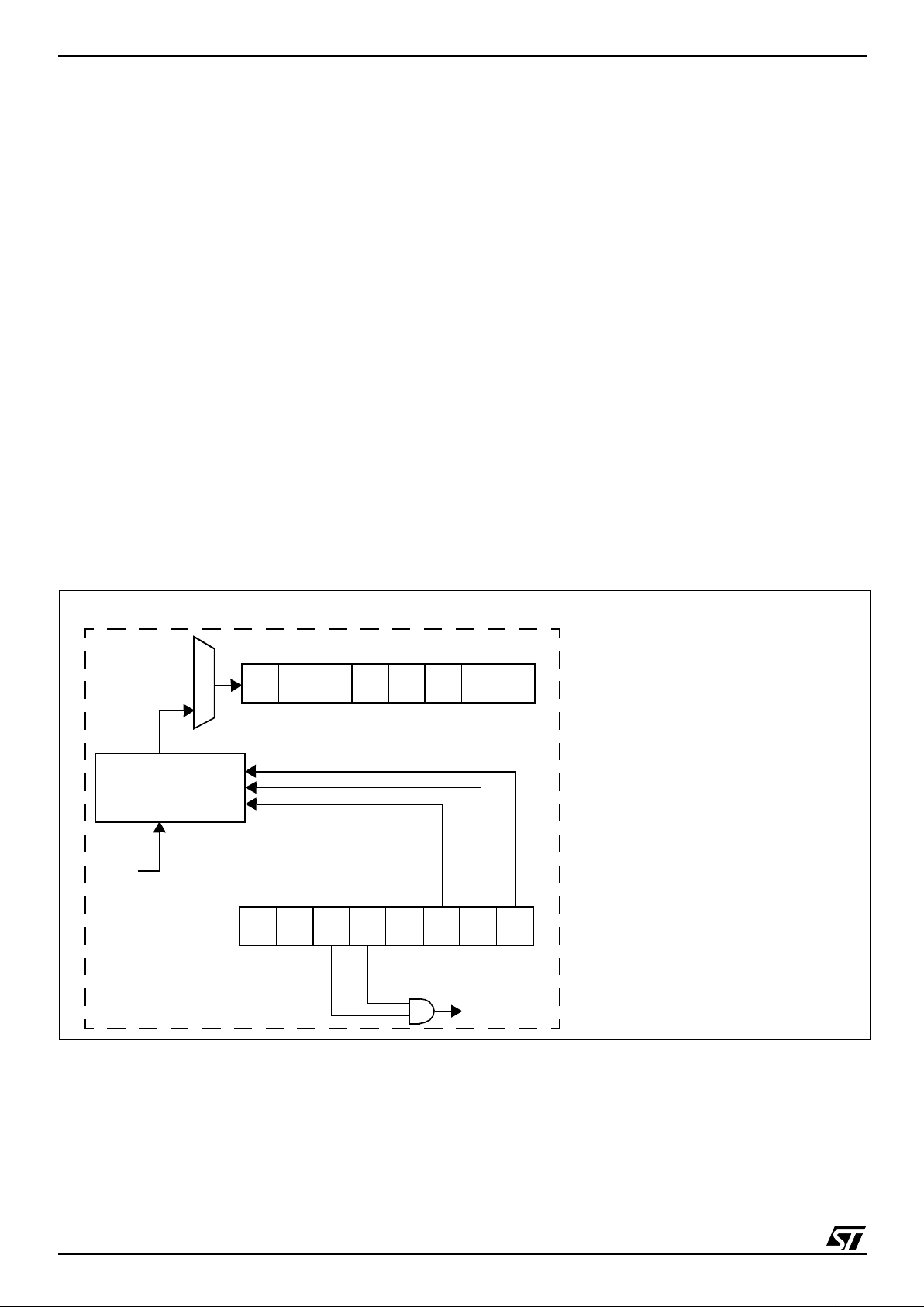
ST7SCR
42/102
12.2 TIME BASE UNIT (TBU)
12.2.1 Introduction
The Timebase unit (TBU) can be used to generate
periodic interrupts.
12.2.2 Main Features
■ 8-bit upcounter
■ Programmable prescaler
■ Period between interrupts: max. 8.1ms (at 8
MHz f
CPU
)
■ Maskable interrupt
12.2.3 Functional Description
The TBU operates as a free-running upcounter.
When the TCEN bit in the TBUCS R register is set
by software, counting starts at the current value of
the TBUCV register. The TBUCV register is incremented at the clock rate output from the prescaler
selected by programming the PR[2:0] bits in the
TBUCSR register.
When the counter rolls over from FFh to 00h, the
OVF bit is s et and an interrupt reques t is generated if ITE is set .
The user can write a value at any time in the
TBUCV register.
12.2.4 Programm ing Ex ampl e
In this example, timer is required to generate an interrupt after a delay of 1 ms.
Assuming that f
CPU
is 8 MHz and a prescaler division factor of 256 will be programmed using the
PR[2:0] bits in the TBUCSR register, 1 ms = 32
TBU timer ticks.
In this case, the initial value to be loaded in the
TBUCV must be (256-32) = 224 (E0h).
ld A, E0h
ld TBUCV, A ; Initialize counter value
ld A 1Fh ;
ld TBUCSR, A ; Prescaler factor = 256,
; interrupt enable,
; TBU enable
Figure 26. TBU Block Diagram
TBU 8-BIT UPCOUNTER (TBUCV REGISTER)
INTERRUPT REQUEST
TBU PRESCALER
f
CPU
TBUCSR REGISTER
PR1 PR0PR2TCENITEOVF
MSB
LSB
0
0
1
TBU
0
1
Page 43
ST7SCR
43/102
TIMEBASE UNIT (Cont’d)
12.2.5 Low Power Mo des
12.2.6 Interrupts
Note: The O VF inte rrupt ev ent is co nnecte d to an
interrupt vector (see Interrupts chapter).
It generates an interrupt if the ITE bit i s set in the
TBUCSR register and the I-bit in the CC register is
reset (RIM instruction).
12.2.7 Register Description
TBU COUNTER VALUE REGISTER (TBUCV)
Read/Write
Reset Value: 0000 0000 (00h)
Bits 7:0 = CV[7:0]
Counter Value
This register contains the 8-bit counter value
which can be read and written anytime by software. It is continuously incremented by hardware if
TCEN=1.
TBU CONTROL/STATUS REGISTER (TBUCSR)
Read/Write
Reset Value: 0000 0000 (00h)
Bits [7:6] = Reserved. Forced by hardware to 0
.
Bit 5 = OVF
Overflow Flag
This bit is set only by ha rdware, when t he count er
value rolls over fr om FFh to 00h. It is cleared by
software reading the TBUCSR register. Writing to
this bit does not change the bit value.
0: No overflow
1: Counter overflow
Bit 4 = ITE
Interrupt enabled.
This bit is set and cleared by software.
0: Overflow interrupt disabled
1: Overflow interrupt enabled. An interrupt request
is generated when OVF=1.
Bit 3 = TCEN
TBU Enable.
This bit is set and cleared by software.
0: TBU counter is frozen and the prescaler is reset.
1: TBU counter and prescaler running.
Bits 2:0 = PR[2:0]
Prescaler Sele cti o n
These bits are set and cleared by software to select the prescaling factor.
Mode Description
WAIT No effect on TBU
HALT TBU halted.
Interrupt
Event
Event
Flag
Enable
Control
Bit
Exit
from
Wait
Exit
from
Halt
Counter Overflow Event
OVF ITE Yes No
70
CV7 CV6 CV5 CV4 CV3 CV2 CV1 CV0
70
0 0 OVF ITE TCEN PR2 PR1 PR0
PR2 PR1 PR0 Prescaler Division Factor
000 2
001 4
010 8
011 16
100 32
101 64
110 128
111 256
1
Page 44

ST7SCR
44/102
12.3 USB INTERFACE (USB)
12.3.1 Introduction
The USB Interface implements a full-speed function interface between the US B and the ST7 microcontroller. It is a highly integrated circuit whi ch
includes the transceiver, 3.3 voltage regulator, SIE
and USB Data Buffer interface. No ex ternal components are needed apart from the external pullup on USBDP for full speed recognition by the
USB host.
12.3.2 Main Features
■ USB Specification Version 1.1 Compliant
■ Supports Full-Speed USB Protocol
■ Seven Endpoints (including default endpoint)
■ CRC generation/checking, NRZI encoding/
decoding and bit-stuffing
■ USB Suspend/Resume operations
■ On-Chip 3.3V Regulator
■ On-Chip USB Transceiver
12.3.3 Functional Description
The block diagram in Figure 27, gives an overview
of the USB interface hardware.
For general information on the USB, refer to the
“Universal Serial Bus Specifications” document
available at http//:www.usb.org.
Serial Interface Engine
The SIE (Serial Interface Engine) interfaces with
the USB, via the transceiver.
The SIE processes tokens, handles data transmission/reception, and handshaking as required by
the USB standard. It al so performs frame formatting, including CRC generation and checking.
Endpoints
The Endpoint registers indicate if the microcontroller is ready to transmit/receive, and how many
bytes need to be transmitted.
Data Transfer to/from USB Data Buffer Memory
When a token for a valid Endpoint is recognized by
the USB interface, the related data transfer takes
place to/from the USB d ata buffer. At the end of
the transaction, an interrupt is generated.
Interrupts
By reading the Interrupt Status register, application software can know which USB eve nt has occurred.
Figure 27. USB Block Diagram
CPU
Transceiver
3.3V
Voltage
Regulator
SIE
ENDPOINT
BUFFER
USB
Address,
and interrupts
USBDM
USBDP
USBVCC
48 MHz
REGISTERS
REGISTERS
data busses
USBGND
BUFFER
USB
DATA
INTERFACE
1
Page 45

ST7SCR
45/102
USB INTERFACE (Cont’d)
USB Endpoint RAM Buffers
There are seven Endpoints includi ng one bidirectional control Endpoint (Endpoint 0), five IN Endpoints (Endpoint 1, 2, 3, 4, 5) and on e OUT endpoint (Endpoint 2).
Endpoint 0 is 2 x 8 bytes in size , End point 1, 3, 4,
and Endpoint 5 are 8 bytes in size and Endpoint 2
is 2 x 64 bytes in size .
Figu re 28. Endpoi nt Buffer Si ze
Endpoint 2 Buffer OUT
Endpoint 1 Buffer IN
Endpoint 0 Buffer IN
Endpoint 0 Buffer OUT
Endpoint 2 Buffer IN
8 Bytes
8 Bytes
8 Bytes
64 Bytes
64 Bytes
Endpoint 3 Buffer IN
8 Bytes
Endpoint 5 Buffer IN
Endpoint 4 Buffer IN
8 Bytes
8 Bytes
1
Page 46

ST7SCR
46/102
USB INTERFACE (Cont’d)
12.3.4 Register Description
INTERRUPT STATUS REGISTER (USBISTR)
Read/Write
Reset Value: 0000 0000 (00h)
These bits cannot be set by software. When an interrupt occurs these bits are set by hardware. Software must read them to determine the interrupt
type and clear them after servicing.
Note: The CTR bit (whi ch is an OR of all the endpoint CTR flags) cannot be cleared directly, only
by clearing the CTR flags in the Endpoint registers.
Bit 7 = CTR
Correct Transfer
.
This bit is set by hardware when a correct transfer
operation is performed. This bit is an OR of all
CTR flags (CTR0 in the EP0R register and
CTR_RX and CTR_TX in the EPnRXR and EPnTXR registers). By looking in the USBSR register, the type of transfer can be determined from the
PID[1:0] bits for Endpoint 0. For the other Endpoints, the Endpoint number on which the transfer
was made is identified by the EP[1:0] bits and the
type of transfer by the IN/OUT bit.
0: No Correct Transfer detected
1: Correct Transfer detected
Note: A t ransfer where the device sent a NAK or
STALL handshake is con sidered not correct (the
host only sends ACK handshakes). A transfer is
considered correct if there are no errors in the PID
and CRC fields, if the DATA0/DATA1 P ID is sent
as expected, if there were no data overruns, bit
stuffing or framing errors.
Bit 6 = Reserved, forced by hardware to 0.
Bit 5 = SO VR Setup Overrun.
This bit is set by hardware when a correct Setup
transfer operation is performed whil e the s oftw are
is servicing an interrupt which occured on the
same Endpoint (CTR0 bit in the EP0R register is
still set when SETUP correct transfer occurs).
0: No SETUP overrun detected
1: SETUP overrun detected
When this event occurs, t he USBSR r egister is not
updated because the only source of the SOVR
event is the SETUP token reception on the Control
Endpoint (EP0).
Bit 4 = ERR
Error
.
This bit is set by hardware whenever one of the errors listed below has occurred:
0: No error detected
1: Timeout, CRC, bit stuffing, nonstandard
framing or buffer overrun error detected
Note: Refer to the ERR[2:0] bits in the USBSR
register to determine the error type.
Bit 3 = SUSP
Suspend mode request
.
This bit is set by hardware when a constant i dle
state is present on the bus line for more than 3 ms,
indicating a suspend mode request from the USB.
The suspend request check is active immediately
after each USB reset event and is disabled by
hardware when sus pend mode is forced (F SUSP
bit in the USBCTLR register) until the end of
resume sequence.
Bit 2 = ESUSP
End Suspend mode
.
This bit is set by hardware when, during suspend
mode, activity is detected that wakes the USB interface up from suspend mode.
This interrupt is serviced by a specific vector, in order to wake up the ST7 from HALT mode.
0: No End Suspend detected
1: End Suspend detected
Bit 1 = RESET
USB reset.
This bit is set by hardware when the USB reset sequence is detected on the bus.
0: No USB reset signal detected
1: USB reset signal detected
Note: The DADDR, EP0R, EP1RXR, EP1TXR,
EP2RXR and EP2TXR registers are reset by a
USB reset.
Bit 0 = SOF
Start of frame.
This bit is set by hardware when a SOF token is received on the USB.
0: No SOF received
1: SOF received
Note: To avoid spurious clearing of some bits, it is
recommended to clear them u sing a load instruction where all bits which must not be altered are
set, and all bits to be cleared are reset. Avoid readmodify-write instructions like AND, XOR...
70
CTR 0 SOVR ERROR SUSP ESUSP RESET SOF
1
Page 47

ST7SCR
47/102
USB INTERFACE (Cont’d)
INTERRUPT MASK REGISTER (USBIMR)
Read/Write
Reset Value: 0000 0000 (00h)
These bits are mask bits for all the interrupt condition bits included in t he US B ISTR regist er. Whenever one of the USBIMR bits is set, if the corresponding USBISTR bit is set, and the I- bit in the
CC register is cleared, an interrupt request is generated. For an explanation of each bit, please refer
to the description of the USBISTR register.
CONTROL REGISTER (USBCTLR)
Read/Write
Reset value: 0000 0110 (06h)
Bit 7 = RSM
Resume Detected
This bit shows when a resume sequence has started on the USB port, requesting the USB interface
to wake-up from suspend state. It can be used to
determine the cause of an ESUSP event.
0: No resume sequence detected on USB
1: Resume sequence detected on USB
Bit 6 = U SB_RST
USB Reset detected
.
This bit shows that a reset sequence has started
on the USB. It can be used to determine the cause
of an ESUSP event (Reset sequence).
0: No reset sequence detected on USB
1: Reset sequence detected on USB
Bits [5:4] = Reserved, forced by hardware to 0.
Bit 3 = RESUME
Resume
.
This bit is set by software to wake-up the Host
when the ST7 is in suspend mode.
0: Resume signal not forced
1: Resume signal forced on the USB bus.
Software should clear this bit after the appropriate
delay.
Bit 2 = PDWN
Power down
.
This bit is set by software to turn off the 3.3V onchip voltage regulator that supplies the external
pull-up resistor and the transceiver.
0: Voltage regulator on
1: Voltage regulator off
Note: After turning on the voltage regulator, software should allow at least 3 µs f or stabilisation of
the power supply before using the USB interface.
Bit 1 = FSUSP
Force suspend mode
.
This bit is set by software to enter Suspend mode.
The ST7 should also be put in Halt mode to reduce
power consumption.
0: Suspend mode inactive
1: Suspend mode active
When the hardware det ects USB a ctivity, it resets
this bit (it can also be reset by soft ware).
Bit 0 = FRES
Force reset.
This bit is set by software to force a reset of the
USB interface, just as if a RESET sequence came
from th e USB.
0: Reset not forced
1: USB interface reset forced.
The USB is held in RESET state until software
clears this bit, at which point a “USB-RE SET” interrupt will be generated if enabled.
70
CTRM 0
SOVR
M
ERRM
SUSPMESUSPMRESET
M
SOFM
70
RSM
USB_
RST
00
RESU
ME
PDWN FSUSP FRES
1
Page 48
ST7SCR
48/102
USB INTERFACE (Cont’d)
DEVICE ADDRESS REGISTER (DADDR)
Read/Write
Reset Value: 0000 0000 (00h)
Bit 7 = Reserved, forced by hardware to 0.
Bits 6:0 = ADD[6:0]
Device address, 7 bits.
Software must write into this register the address
sent by the host during enumeration.
Note: This register is also reset when a USB reset
is received or forced throug h bit FRE S in the US BCTLR register.
USB STATUS REGISTER (USBSR)
Read only
Reset Value: 0000 0000 (00h)
Bits 7 :6 = PID[1:0]
Token PID bits 1 & 0 for End-
point 0 Control
.
USB token PIDs are encoded in four bits. PID[1:0]
correspond to the most significant bits of the PID
field of the last token PID received by Endpoint 0.
Note: The least significant PID bits have a fixed
value of 01.
When a CTR interrupt occurs on Endpoint 0 (see
register USBISTR) the software should read the
PID[1:0] bits to retrieve the PID name of t he toke n
received.
The USB specification defines PID bits as:
Bit 5 = IN/OUT
Last transaction direction for E nd-
point 1, 2 , 3, 4 or 5 .
This bit is set by hardware when a CTR interrupt
occurs on Endpoint 1, 2, 3, 4 or 5.
0: OUT transaction
1: IN transaction
Bits 4:3 = Reserved, forced by hardware to 0.
Bits 2:0 = EP[2:0]
Endpoint number.
These bits identify the endpoint which required attention.
000 = Endpoint 0
001 = Endpoint 1
010 = Endpoint 2
011 = Endpoint 3
100 = Endpoint 4
101 = Endpoint 5
ERROR STATUS REGISTER (ERRSR)
Read only
Reset Value: 0000 0000 (00h)
Bits 7:3 = Reserved, forced by hardware to 0.
Bits 2:0 = ERR[2:0]
Error type
.
These bits identify the type of error which occurred.
Note: these bits are set by hardware when an error interrupt occurs and are reset automatically
when the error bit (USBISTR bit 4) is cleared by
software.
70
0 ADD6ADD5ADD4ADD3ADD2ADD1ADD0
70
PID1 PID0
IN/
OUT
0 0 EP2 EP1 EP0
PID1 PI D0 PID Name
00 OUT
10 IN
1 1 SETUP
70
00000ERR2ERR1ERR0
ERR2 ERR1 ERR 0 Me aning
0 0 0 No error
0 0 1 Bitstuffing error
0 1 0 CRC error
011
EOP error (unexpected end of
packet or SE0 not followed by
J-state)
100
PID error (PID encoding error,
unexpected or unknown PID)
101
Memory over / underrun (memory controller has not answered in time to a memory
data request)
111
Other error (wrong packet,
timeout error)
1
Page 49

ST7SCR
49/102
USB INTERFACE (Cont’d)
ENDPOINT 0 REGISTER (EP0R)
Read/Write
Reset value: 0000 0000(00h)
This register is used for contro lling Endp oint 0.
Bits 6:4 and bits 2: 0 are also reset by a USB reset,
either received from the USB or forced through the
FRES bit in USBCTLR.
Bit 7 = CTR0
Correct Transfer
.
This bit is set by hardware when a correct transfer
operation is performed on Endpoint 0. This bit
must be cleared after the corresponding interrupt
has been serviced.
0: No CTR on Endpoint 0
1: Correct transfer on Endpoint 0
Bit 6 = DTOG_TX
Data Toggle, for transmission
transfers
.
It contains the required value of the toggle bit
(0=DATA0, 1=DATA1) for the next transmitted
data packet. This bit is set by hardware on reception of a SETUP PID. DTOG_TX toggles only
when the transmitter has received the ACK signal
from the USB host. DTOG_TX and also
DTOG_RX are normally updat ed b y hardware, on
receipt of a relevant PID. They can be also written
by the user, both for testing purposes and to force
a specific (DATA0 or DATA1) token.
Bits 5:4 = STAT_TX [1:0]
Status bits, for transmis-
sion transfers
.
These bits contain the information about the endpoint status, which are listed below
Table 15. Transmission Status
Encoding
These bits are written b y s oftware. Hardware s ets
the STAT_TX and STAT_RX bits to NAK when a
correct transfer has occurred (CTR=1) addressed
to this endpoint; this allows software to prepare the
next set of data to be transmitted.
Bit 3 = Reserved, forced by hardware to 0.
Bit 2 = DTOG_RX
Data Toggle, for reception
transfers
.
It contains the expected value of the toggle bit
(0=DATA0, 1=DATA1) for the next data packet.
This bit is cleared by hardware in the first stage
(Setup Stage) of a control transfer (SETUP transactions start always with DATA0 PID). The receiver toggles DTOG_ RX only if it receives a correct
data packet and the packet’s data PID matches
the receiver sequence bit.
70
CTR0
DTOG
_TX
STAT_
TX1
STAT_
TX0
0
DTOG
_RX
STAT_
RX1
STAT_
RX0
STAT_TX1 STAT_TX0 Meaning
00
DISABLED: no function can be
executed on this endpoint and
messages related to this endpoint are ignored.
01
STALL: the endpoint is stalled
and all transmission requests
result in a STALL handshake.
10
NAK: the endpoint is NAKed
and all transmission requests
result in a NAK handshake.
11
VALID: this endpoint is enabled
(if an address match occurs, the
USB interface handles the
transaction).
1
Page 50

ST7SCR
50/102
USB INTERFACE (Cont’d)
Bits 1:0 = STAT_RX [1:0]
Status b its , for rece ption
transfers
.
These bits contain the information abo ut the e ndpoint status, which are listed below:
Table 16. Reception Status Encoding
These bits are written by softw are. Hardware set s
the STAT_RX and STAT_ TX bits to NAK when a
correct transfer has occurred (CTR =1) addressed
to this endpoint, so the software has the t ime to examine the received data before acknowledging a
new transaction.
Note 1:
If a SETUP transaction is received while the status
is different from DISABLED, it is acknowleded and
the two directional status bits are set to NAK by
hardware.
Note 2:
When a STALL is answered by the USB device,
the two directional status bits are set to S T ALL by
hardware.
ENDPOINT TRANSMISSION REGISTER
(EP1TXR, EP2TXR, EP3TXR, EP4TXR,
EP5TXR)
Read/Write
Reset value: 0000 0000 (00h)
This register is used for controlling Endpoint 1, 2,
3, 4 or 5 transmission. B its 2 :0 are also reset by a
USB reset, either received from the USB or forced
through the FRES bit in the USBCTLR register.
Bits [7:4] = Reserved, forced by hardware to 0.
Bit 3 = CTR_TX
Correct Transmission Transfer
.
This bit is set by hardware when a correct transfer
operation is performed in transmission. This bit
must be cleared after the corresponding interrupt
has been serviced.
0: No CTR in transmission on Endpoint 1, 2, 3, 4 or
5
1: Correct transfer in transmission on Endpoint 1,
2, 3, 4 or 5
Bit 2 = DTOG_TX
Data Toggle, for t ransmission
transfers
.
This bit contains the required value of the toggle
bit (0=DATA0, 1=DATA1) for the next data packet.
DTOG_TX toggles onl y when the transmitter has
received the ACK signal from the USB host.
DTOG_TX and DTOG_RX are normally updated
by hardware, at the receipt of a relevant PID. They
can be also written by the user, both for testing
purposes and to force a specific (DATA0 or
DATA1) token.
Bits [1:0] = STAT_TX [1:0]
Status bits, for trans-
mission transfers
.
These bits contain the information about the endpoint status, which is listed below
Table 17. Transmission Status Encoding
These bits are written by software, but hardware
sets the STAT_TX bits to NAK when a correct
transfer has occurred (CTR=1) addressed to this
endpoint. This allows software to prepare the next
set of data to be transmitted.
STAT_RX1 STAT_RX0 Meaning
00
DISABLED: no function can be
executed on this endpoint and
messages related to this endpoint are ignored.
01
STALL: the endpoint is stalled
and all reception requests result in a STALL handshake.
10
NAK: the endpoint is NAKed
and all reception requests result in a NAK handshake.
11
VALID: this endpoint is enabled (if an address match occurs, the USB interface
handles the transaction).
70
0000
CTR_TXDTOG
_TX
STAT_
TX1
STAT_
TX0
STAT_TX1 STAT_TX0 Meaning
00
DISABLED: transmission
transfers cannot be executed.
01
STALL: the endpoint is stalled
and all transmission requests
result in a STALL handshake.
10
NAK: the endpoint is naked
and all transmission requests
result in a NAK handshake.
11
VALID: this endpoint is enabled for transmission.
1
Page 51

ST7SCR
51/102
USB INTERFACE (Cont’d)
ENDPOINT 2 RECEPTION REGISTER
(EP2RXR)
Read/Write
Reset value: 0000 0000 (00h)
This register is used for controlling Endpoint 2 reception. Bits 2:0 are also reset by a USB reset, either r ecei ve d from the USB o r fo rced throu gh the
FRES bit in the USBCTLR register.
Bits [7:4] = Reserved, forced by hardware to 0.
Bit 3 = C TR_RX
Reception Correct Transfer
.
This bit is set by hardware when a correct transfer
operation is performed in reception. This bit must
be cleared after that the corresponding interrupt
has been serviced.
Bit 2 = DTOG_RX
Data Toggle, for reception
transfers
.
It contains the expected value of the toggle bit
(0=DATA0, 1=DATA1) for the next data packet.
The receiver toggles DTOG_RX only if it receives
acorrect data packet and the packet’s data PID
matches the receiver sequence bit.
Bits [1:0] = STAT_RX [1:0]
Status bits, for recep-
tion transfers
.
These bits contain the information about the endpoint status, which is listed below:
Table 18. Reception Status Encoding
These bits are written by software, but hardware
sets the STAT_RX bits to NAK when a correct
transfer has occurred (CTR=1) addressed to this
endpoint, so the software has the time to examine
the received data before acknowledging a new
transaction.
70
0000
CTR_RXDTOG
_RX
STAT_
RX1
STAT_
RX0
STAT_RX1 STAT_RX0 Meaning
00
DISABLED: reception transfers cannot be executed.
01
STALL: the endpoint is stalled
and all reception requests result in a STALL handshake.
10
NAK: the endpoint is naked
and all reception requests result in a NAK handshake.
11
VALID: this endpoint is enabled for reception.
1
Page 52

ST7SCR
52/102
USB INTERFACE (Cont’d)
RECEPTION COUNTER REGISTER (CNT0RXR)
Read/Write
Reset Value: 0000 0000 (00h)
This register contains the al located buff er size for
endpoint 0 reception, setting the maximum
number of bytes the related endpo int can receive
with the next OUT or SETUP transaction. At the
end of a reception, the value of this register is th e
max size decremented by the num ber of b ytes received (to determine the number of bytes received, the software must subtract the content of
this register from the allocated buffer size).
TRANSMISSION COUNTER REGISTER
(CNT0TXR, CNT1TXR, CNT3TXR, CNT4TXR,
CNT5TXR)
Read/Write
Reset Value 0000 0000 (00h)
This register contains the number of bytes to b e
transmitted by Endpo int 0, 1, 3, 4 or 5 at the nex t
IN token addressed to it.
RECEPTION COUNTER REGISTER (CNT2RXR)
Read/Write
Reset Value: 0000 0000 (00h)
This register contains the allocated b uffer size for
endpoint 2
reception, setting the maximum
number of bytes the related end point can receive
with the next OUT transact ion. At the end of a reception, the value of this register is the max size
decremented by the number of bytes received (t o
determine the num ber of bytes received, the sof tware must subtract the content of t his register f rom
the allocated buffer size).
TRANSMISSION COUNTER REGISTER
(CNT2TXR)
Read/Write
Reset Value 0000 0000 (00h)
This register co ntai ns the number of bytes to be
transmitted by Endpoint 2 at the next IN tok en addressed to it.
70
0 0 0 0 CNT3 CNT2 CNT1 CNT0
70
0 0 0 0 CNT3 CNT2 CNT1 CNT0
70
0 CNT6 CNT5 CNT4 CNT3 CNT2 CNT CNT0
70
0 CNT6 CNT5 CNT4 CNT3 CNT2 CNT1 CNT0
1
Page 53

ST7SCR
53/102
USB INTERFACE (Cont’d)
Table 19. USB Register Map and Reset values
Address
(Hex.)
Register
Name
76543210
20
USBISTR
Reset Va l ue
CTR
0
0
0
SOVR
0
ERR
0
SUSP
0
ESUSP
0
RESET
0
SOF
0
21
USBIMR
Reset Va l ue
CTRM
0
0
0
SOVRM
0
ERRM
0
SUSPM0ESUSPM0RESETM
0
SOFM
0
22
USBCTL R
Reset Va l ue
RSM0USB_RST
0
00
RESUME0PDWN
1
FSUSP
1
FRES
0
23
DADDR
Reset Va l ue
0
ADD6
0
ADD5
0
ADD4
0
ADD3
0
ADD2
0
ADD1
0
ADD0
0
24
USBSR
Reset Va l ue
PID1
0
PID0
0
IN /OUT
0
00
EP2
0
EP1
0
EP0
0
25
EP0R
Reset Va l ue
CTR00DTOG_TX0STAT_TX10STAT_TX0
0
0
0
DTOG_RX0STAT_RX10STAT_RX0
0
26
CNT0RX R
Reset Va l ue
00 0 0
CNT3
0
CNT2
0
CNT1
0
CNT0
0
27
CNT0TXR
Reset Va l ue
00 0 0
CNT3
0
CNT2
0
CNT1
0
CNT0
0
28
EP1TXR
Reset Va l ue
00 0 0
CTR_TX0DTOG_TX0STAT_TX10STAT_TX0
0
29
CNT1TXR
Reset Va l ue
00 0 0
CNT3
0
CNT2
0
CNT1
0
CNT0
0
2A
EP2RXR
Reset Va l ue
00 0 0
CTR_RX0DTOG_RX0STAT_RX10STAT_RX0
0
2B
CNT2RX R
Reset Va l ue
0
CNT6
0
CNT5
0
CNT4
0
CNT3
0
CNT2
0
CNT1
0
CNT0
0
2C
EP2TXR
Reset Va l ue
00 0 0
CTR_TX0DTOG_TX0STAT_TX10STAT_TX0
0
2D
CNT2TXR
Reset Va l ue
0
CNT6
0
CNT5
0
CNT4
0
CNT3
0
CNT2
0
CNT1
0
CNT0
0
2E
EP3TXR
Reset Va l ue
00 0 0
CTR_TX0DTOG_TX0STAT_TX10STAT_TX0
0
2F
CNT3TXR
Reset Va l ue
00 0 0
CNT3
0
CNT2
0
CNT1
0
CNT0
0
30
EP4TXR
Reset Va l ue
00 0 0
CTR_TX0DTOG_TX0STAT_TX10STAT_TX0
0
31
CNT4TXR
Reset Va l ue
00 0 0
CNT3
0
CNT2
0
CNT1
0
CNT0
0
32
EP5TXR
Reset Va l ue
00 0 0
CTR_TX0DTOG_TX0STAT_TX10STAT_TX0
0
1
Page 54

ST7SCR
54/102
33 CNT5TXR 0 0 0 0
CNT3
0
CNT2
0
CNT1
0
CNT0
0
34 ERRSR 0 0 0 0 0
ERR2
0
ERR1
0
ERR0
0
Address
(Hex.)
Register
Name
76543210
1
Page 55
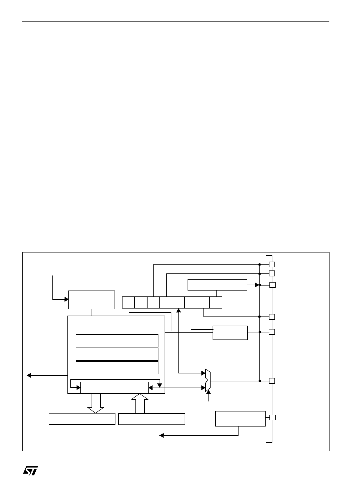
ST7SCR
55/102
12.4 SMARTCARD INTERFACE (CRD)
12.4.1 Introduction
The Smartcard Interface (CRD) provides all the required signals for acting as a smartcard interface
device.
The interface is electrically compatible with (and
certifiable to) the ISO7816, EMV, GSM and WHQL
standards.
Both synchronous (e.g. memory cards) and asynchronous smartcards (e.g. microprocessor cards)
are supported.
The CRD generates the required voltages to be
applied to the smartcard lines.
The power-off sequence is managed by the CRD.
Card insertion or card removal is detected by the
CRD using a card presence switch connected to
the external CRDDET pin. If a card is removed, the
CRD automatically deactivates the smartcard using the ISO7816 deactivation sequence.
An maskable interrupt is generated when a card is
inserted or removed.
Any malfunction is reported to the mi crocontroller
via the Smartcard Interrupt Pending Register
(CRDIPR) and Smartcard Status (CRDSR) Registers.
12.4.2 Main features
■ Support for ISO 7816-3 standard
■ Character mode
■ 1 transmit buffer and 1 receive buffer
■ 4-Mhz fixed card clock
■ 11-bit etu (elementary time unit) counter
■ 9-bit guardtime counter
■ 24-bit general purpose waiting time counter
■ Parity generation and checking
■ Automatic character repetition on parity error
detection in transmission mode
■ Automatic retry on parity error detection in
reception mode
■ Card power-off deactivation sequence
generation
■ Manual mode for driving the card I/O directly for
synchronous protocols
12.4.3 Functional Description
Figure 29 gives an overview of the smartcard inter-
face.
Figure 29. Smartcard Interface Block Diagram
CLK
SEL
CRD
CLK
CRDCCR
IO
CRD
CRD CRD
RST VCC
C8
CRD
C4
CRD
CRDIO
CRDC4
CRDC8
CRDRST
CRDCLK
CRDDET
0
1
UART SHIFT REGISTE R
CRDRXB
CRDTXB
UART RECEIVE BUFFER
UART TRANSMIT BUFFER
CARD DETECTION
CARD INSERTION/
CRDVCC
POWER-OFF LOGIC
CLOCK
CONTROL
UART BIT
11-BIT
4 MHz
ETU COUNTER
9-BIT GUARDTIME COUNTER
24-BIT WAITING TIME COUNTER
PARITY GENERATION/CHECKING
COMMUNICATIONS CONTROL
CRD INTERRUPT
LOGIC
REMOVAL INTERRUPT
1
Page 56

ST7SCR
56/102
SMARTCARD INTERFACE (Cont’d)
12.4.3.1 Power Supply Ma nag eme nt
Smartcard Power Supply Selection
The Smartcard interface consists of a powe r supply output on the CRDVCC pin and a set of card interface I/Os which are powered by the same rail.
The card voltage (CRDVCC) is user programmable via the VCARD [1:0] bits in the CRDCR register (refer to the Smartcard Interface section).
Four voltage values can be selected:
5V, 3 V, 1.8 V or 0V.
Current Overload Detection and Card Removal
For each voltage, when an overload current is detected (refer to Section 12.4 on page 55), or whe n
a card is removed, the CRDVCC power supply
output is directly connected to ground.
12.4.3.2 I/O Driving Modes
Smartcard I/Os are driven in two principal modes:
– UART mode (i.e. when the UART bit of the
CRDCR register is set)
– M anua l mode , driven directly by software using
the Smartcard Contact register (i.e. when the
UART bit of the CRDCR register is reset).
Card power-on activation must driven by software.
Card deactivation is handled autom atically by the
Power-off functional state machine hardware.
12.4.3.3 UART Mode
Two registers are connected to the UART shift
register: CRDTXB for transmission a nd CRDRXB
for reception. They act as buffers to off-load the
CPU.
A parity checker and generator is coupled to the
shift er.
Character repetition and retry are supported.
The UART is in reception mode by default and
switches automatically to transmission mode
when a byte is written in the buffer.
Priority is given to transmission.
Elementary Time Unit Counter
This 11-bit counter controls the working frequency
of the UART. The operating frequency of the clock
is the same as the card clock frequency (i.e. 4
MHz).
A compensation mode can be activated via the
COMP bit of the CRDETU1 register to allow a frequency granularity down to a half-etu.
Note: The decimal value is li mited to a half clock
cycle. The bit duration is not fixed. It alternates between n clock cycles and n-1 cl ock cycl es, where n
is the value to be written in the CRDETU register.
The character duration (10 bits) is also equal to
10*(n - ½) clock cycles This is preci se enough to
obtain the character duration specified by the
ISO7816-3 standard.
For example, if F=372 and D=32 (F being the clock
rate conversion factor and D the baud rate adjustment), then etu =11.625 clock cycles.
To achieve this clock rate, compensation mode
must be activated and the etu duration must be
programmed to 12 clock cycles.
The result will be an average character duration of
11.5 clock cycles (for 10 bits).
See Figure 30.
Guardtime counter
The guardtime counter is a 9-bit counter which
manages the character frame. It controls the duration between two consecutive characters in transmission.
It is incremented at the etu rate.
No guardtime is inserted for the first character
transmitted.
The guardtime between the last byte received
from the card and the next byte transmitted by the
reader must be handled by software.
1
Page 57

ST7SCR
57/102
Figure 30. Compensation Mode
12cy
11cy
12cy
11cy
12cy
11cy
12cy
11cy
12cy
11cy
Start bit
Data bits
Parity bit
UART
CRDIO
Working Clock
F=372
D= 32
1
Page 58

ST7SCR
58/102
SMARTCARD INTERFACE (Cont’d)
Waiting Time Counter
The Waiting Time counter is a 24-bit counter used
to generate a timeout signal.
The elementary time unit counter acts as a prescaler to the Waiting Time counter which is incremented at the etu rate.
The Waiting Time Counter can be used in both
UART mode and Manual mode and acts in different ways depending on the selected mode.
The CRDWT2, CRDWT1 and CRDWT0 are load
registers only, the counter itself is not directly access ib le.
UART Mode
The load conditions are either:
– A Start bit is detected while UART bit =1 and the
WTEN bit =1.
or
– A write access to the CRDWT2 register is per-
formed while the UART bit = 1 and the WTEN bit
= 0. In this case, the Waiting Time counter can be
used as a general purpose timer.
In UART mode, if the WTEN bit of the CRDCR reg-
ister is set, the counter is loaded automa tically on
start bit detection. Software can change the time
out value on-the-fly by writing to the
CRDWT registers. For example, in T=1 mode,
software must load the Block Waiting Time (BWT)
time-out in the CRDWT registers before the start
bit of the last transmitted character.
Then, after transmission of this l ast character, signalled by the TXC interrupt, software must write
the CWT value (Character Waiting Time) in the
CRDWT registers. See example in Figure 31.
Manual m o de
The load conditions are:
– A write access to the CRDWT2 register is per-
formed while the UART bit = 0 and the WTEN bit
= 0
In Manual mode, if the WTEN bi t of th e CRDCR
register is reset, the timer acts as a general purpose timer. The timer is loade d when a write access to the CRDWT2 register occurs. The timer
starts when the WTEN bit = 1.
12.4.3.4 Interrupt generator
The Smartcard Interface has 2 interrupt vectors:
– Card Insertion/Removal Interrupt
– CRD Interrupt
The CRD interrupt is cleared when software reads
the CRDIPR register. The Card Insertion/Removal
is an external interrupt and is cleared automatically by hardware at the end of the interrupt service
routine (IRET instruction).
If an interrupt occurs while the CRDIPR register is
being read, the corresponding bit will be set by
hardware after the read access is done.
Figure 31. Waiting Time Counter Example
BWT
CWT
Reader
Smartcard
Firmware must program BWT
Firmware must program CWT
TXC Interrupt
Start bit
Waiting Time Counter
loaded on start bit
CHAR0
CHAR1
CHARn
CHAR0 CHAR1
1
Page 59

ST7SCR
59/102
SMARTCARD INTERFACE (Cont’d)
12.4.3.5 Card detection mechanism
The CRDDET bit in the CRDCR Register indicates
if the card presence detector (card switch) is open
or closed when a card is inserted. When the
CRDIRF bit of the CRDSR is set, it indicates that a
card is present.
To be able to po wer-on the smart card, card presence is mandatory. Removing the smartcard will
automatically start the ISO7816-3 card deactivation sequence (see Section 12.4 .3.6).
There is no hardware debouncing: The CRDIRF
bit changes whenever the level on the CRDDET
pin changes. The card switch can generate an interrupt which can be used to wake up the device
from suspend mode and for software debouncing.
Three different cases can occur:
– T he microcon troller is in run mode, waiting for
card insertion:
Card insertion generates an interrupt and the
CRDIRF bit in the CRDSR register is set. Debouncing is managed by software. After the time
required for debouncing, if the CRDIRF bit is set,
the CRDVCC bit in the CRDCR register is set by
software to apply the selected voltage to the
CRDVCC pin
– The microcontroller is in suspend mode and a
card is inserted:
The ST7 is woken up by the interrupt. The card
insertion is then handled in the same way as in
the previous case.
– The card is removed:
– The CRDIRF bit is reset without hardware de-
bouncing
– A Card Insertion/Removal interrupt is generat-
ed, (if enabled by the CRDIRM bit in the
MISCR2 register)
– The CRDVCC bit is immediately reset by
hardware, starting the card deactivation sequence.
Figure 32. Card det ection block diagra m
CRDDET
CRD
CRDSR
1
0
CARD INSERTION/REMOVAL
0
7
IRF
DET
CRDCR
0
7
CNF
CRD
MISCR2
0
7
IRM
Pull-up
EDGE DETECTOR
Interrupt Request
SMARTCARD INTERFACE (CRD)
1
Page 60

ST7SCR
60/102
SMARTCARD INTERFACE (Cont’d)
12.4.3.6 Card Deactivation Sequence
This sequence can be activated in two different
ways:
– A utom atica lly as soon as the card presence de-
tector detects a card removal (via t he CRDIRF bit
in the CRDSR register, refer to Section 12.4.3.5).
– By software, writing the CRDVCC bit in the CRD-
CR register, for example:
– If there is a smartcard current overflow (i.e.
when the IOVFF bit in the CRDSR reg ister is
set)
– If the voltage is not wi thin the s pe cified range
(i.e. when the VCARDOK bit in the CRDSR
register is cleared), but software must clear
the CRDVCC bit in the CRDCCR register to
start the deactivation sequence.
When the CRDVCC bit is cleared, this starts the
deactivation sequence. CRDCLK, CRDIO,
CRDC4 and CRDC8 pins are then deactivated as
shown in Figure 33:
Figure 33. Card deactivation sequence
Figure 34. C ard v ol ta ge sel e ct io n an d power OFF bl ock di ag ra m
CRDVCC pin
CRDRST pin
CRDCLK pin
CRDIO pin
CRDC4 pin
CRDC8 pin
8 CPU Clk cycles
CRDVCC
CRD
CRDCCR
BLOCK
0
7
VCC
CRDCR
07
IRF
CRDSR
0
7
CRD
VCARD
1
POWER OFF
IOVF
OK
CRDIER
0
7
CRDIPR
0
7
IOVP
VCRD
SMARTCARD
POWER SUPPLY
BLOCK
5V
VCARDOK Interrupt Request
IOVF Interrupt Request
2
2
Card voltage selection
2
IOVM
VCRD
P
M
VCARD
0
VCARD
1
Page 61

ST7SCR
61/102
SMARTCARD INTERFACE (Cont’d)
Figure 35. Power Off Timing Diagram
Note: Refer to the Electrical Characteristics section for the values of t
ON
and t
OFF
.
Figure 36. Card clock selection block diagram
1100
00
VCARD[1:0]
CRDVCC
VCARDOK
VCRDP Interrupt
V
CARDOK
11
VCRDP Interrupt
Software Power-Off
Voltage Error
Power-On
Power-On
t
OFF
t
ONt
ON
t
OFF
0.4V
CLK
4 MHz
1
0
SEL
CRD
CLK
CRDCCR
POWER OFF
BLOCK
CRDCLK
ISOCLK
DIV
PLLPLL
OSC
4 MHz
1
Page 62

ST7SCR
62/102
SMARTCARD INTERFACE (Cont’d)
12.4.4 Register Description
SMARTCARD INTERFACE CONTROL REGISTER (CRDCR)
Read/Write
Reset Value: 0000 0000 (00h)
Bit 7 = C RDRST
Smartcard Interface Reset.
This bit is set by software to reset the UART of the
Smartcard interface.
0: No Smartcard UART Reset
1: Smartcard UART Reset
Bit 6 = CRDDET
Card Presence Detector.
This bit is set and cleared by software to configure
the card presence detector switch.
0: Switch open if no card is present
1: Switch closed if no card is present
Bits [5:4] = VCARD[1:0]
Card voltage selection.
These bits select the card voltage.
Bit 3 = U ART
UART Mode Selection.
This bit is set and cleared by software to select
UART or manual mode.
0: CRDIO pin is a copy of the CRDIO bit in the
CRDCCR register (Manual mode).
1: CRDIO pin is the output of the smartcard UART
(UART mode).
Caution: Before switching from Manual mode to
UART mode, software must se t th e CRDIO bit in
the CRDCCR register.
Bit 2 = WTEN
Waiting Time Counter enable.
0: Waiting Time counter stopped. While WTEN =
0, a write access to the CRDWT2 register loads
the Waiting time counter with the load value held
in the CRDWT0, CRDWT1 and CRDWT2 registers.
1: Start counter. In UART mode, the counter is au-
tomatically reloaded on start bit detection.
Bit 1 = CREP
Automatic character repetition in
case of parity error.
0: In reception mode: no parity error signal indica-
tion (no retry on parity error).
In transmission mode: no error signal processing. No retransmission of a refused character on
parity error.
1: Automatic parity management:
In transmission mode: up to 4 character repetitions on parity error.
In reception mode: up to 4 retries are made on
parity error.
The PARF parity error flag is set by hardwa re if a
parity error is detected.
If the transmitted character is refused, the PARF
bit is set (but the TXCF bit is reset) and an interrupt
is generated if the PARM bit is set.
Note: If CREP=1, the PARF flag is set at the 5th
error (after 4 character repetitions or 4 retries).
If CREP=0, the PARF bit is set after the first parity
error.
Bit 0 = CONV
ISO convention selection.
0: Direct convention, the B0 bit (LSB) is sent first, a
’1’ is a level 1 on the Card I/O pin, the parity bit is
added after the B7 bit.
1: Inverse convention, the B7 bit (MSB) is sent
first, a ’1’ is a level 0 on Card I/O pin, the parity
bit is added after the B0 bit.
Note: To detect the convention used by any card,
apply the following rule. If a card uses the convention selected by the reader, an RXC event occurs
at answer to reset. Otherwise a parity error also
occurs.
70
CRD
RST
CRD
DET
VCAR
D 1
VCAR
D 0U ART
WT ENC
REP
CO
NV
Bit 1 Bit 0 Vcard
00 0V
0 1 1.8V
10 3V
11 5V
1
Page 63

ST7SCR
63/102
SMARTCARD INTERFACE (Cont’d)
SMARTCARD INTERFACE STATUS REGISTER
(CRDSR)
Read only (Read/Write on some bits)
Reset Value: 1000 0000 (80h)
Bit 7 =TxBEF
Transmit Buffer Empty Flag.
- Read only
0: Transmit buffer is not empty
1: Transmit buffer is empty
Bit 6 = C RDIRF
Card Insertion/Removal Flag.
- Read only
0: No card is present
1: A card is present
Bit 5 = IOVF
Card Overload Current Flag.
- Read only
0: No card overload current
1: Card overload current
Bit 4 = V CARDOK
Card voltage status Flag.
- Read only
0: The card voltage is not in the specified range
1: The card voltage is within the specified range
Bit 3 = WTF
Waiting Time Counter overflow Flag.
- Read only
0: The WT Counter has not reached its maximum
value
1: The WT Counter has reached its maximum val-
ue
Bit 2 = TXCF
Transmitted character Flag.
- Read/Write
This bit is set by hardware and cleared by software.
0: No character transmitted
1: A character has been transmitted
Bit 1 = RXCF
Received character Flag.
- Read only
This bit is set by hardware and cleared by hardware when the CRDRXB buffer is read.
0: No character received
1: A character has been received
Bit 0 = PARF
Parity Error Flag.
- Read/Write
This bit is set by hardware and cleared by software.
0: No parity error
1: Parity error
Note: When a character is received, the RXCF bit
is always set.When a character is received with a
parity error, the PARF bit is also set.
70
TXBE
F
CRD
IRF
IOVF
VCARD
OK
WTF
TXCFRXCFPAR
F
Page 64

ST7SCR
64/102
SMARTCARD INTERFACE (Cont’d)
SMARTCARD CONTACT CONTROL REGISTER
(CRDCCR)
Read/Write
Reset Value: 00xx xx00 (xxh)
Note: To modify the content of this register, the LD
instruction must be used (do not use the BSET
and BRES instructions).
Bit 7 = C LKSEL
Card clock selection.
This bit is set and cleared by software.
0: The signal on the CRDCLK pin is a copy of the
CRDCLK bit.
1: The signal on the CRDCLK pin is a 4MHz fre-
quency clock.
Note: To start the clock at a known level, the CRDCLK bit should be changed before the CLKSEL
bit.
Bit 6 = Reserved, must be kept cleared.
Bit 5 = C RDC8
CRDC8 pin control.
Reading this bit returns the value present on the
CRDC8 pin. Writing this bit outputs the bit value on
the pin.
Bit 4 = C RDC4
CRDC4 pin control
Reading this bit returns the value present on the
CRDC4 pin. Writing this bit outputs the bit value on
the pin.
Bit 3 = CRDIO
CRDIO pin control
.
This bit is active only if the UART bit in the CRDCR
Register is reset. Reading this bit returns the value
present on the CRDIO pin.
If the UART bit is reset:
– Writing “0” forces a low level on the CRDIO pin
– Writing “1” forces the CRDIO pin to open drain
Hi-Z.
Bit 2 = CRDCLK
CRDCLK pin control
This bit is active only if the CLKSEL bit of the CRDCCR register is reset. Reading this bit returns the
value present in the register (not the CRDCLK pin
value).
When the CLKSEL bit is reset:
0: Level 0 to be applied on CRDCLK pin.
1: Level 1 to be applied on CRDCLK pin.
Note: To ensure that the clock stops at a given
value, write the desired value in the CRDCLK bit
prior to changing the CLKSEL bit from 1 to 0.
Bit 1 = CRDRST
CRDRST pin control.
Reading this bi t returns the value present on the
CRDRST pin. Writing this bit outputs the bit value
on the pin.
Bit 0 = CRDVCC
CRDVCC Pin Control.
This bit is set and cleared by sof tware and forced
to 0 by hardware when no card is present
(CRDIRF bit=0).
0: No voltage to be applied on the CRDVCC pin.
1: The selected voltage must be applied on the
CRDVCC pin.
Figure 37. Smartcard I/O Pin Structure
70
CLK
SEL
- CRD C8CRD C4CRD IOCRD
CLK
CRD
RST
CRD
VCC
I/O PIN
DAT A BUS
CRDCCR
REGIS T E R
Page 65

ST7SCR
65/102
SMARTCARD INTERFACE (Cont’d)
SMARTCARD ELEMENTARY TIME UNIT REG-
ISTER (CRDETUx)
CRDETU1
Read/Write
Reset Value: 0000 0001 (01h)
Bit 7 = COMP
Elementary Time Unit Comp ensa-
tion .
0: Compensation mode disabled.
1: Compensation mode enabled. To allow non in-
teger value, one clock cycle is subtracted from
the ETU value on odd bits. See Figure 30.
Bit [6:3] = Reserved
Bits 2 :0 = ETU [10:8]
ETU value in card clock cy-
cles.
Writing CRDETU1 register reloads the ETU counter.
CRDETU0
Read/Write
Reset Value: 0111 0100 (74h)
Bits 7:0 = ETU [7:0]
ETU value in card clock cy-
cles .
Note: The value of ETU [10:0] must in the range
12 to 2047. To write 2048, clear all the bits.
GUARDTIME REGISTER (CRDGTx)
CRDGT1
Read/Write
Reset Value: 0000 0000 (00h)
CRDGT0
Read/Write
Reset Value: 0000 1100 (0Ch)
Software writes the Guardtime v alue in this register. The value is loaded at the end of the current
Guard period.
GT: Guard Time: Minimum time between two consecutive start bits in transmission mode. Value expressed in Elementary Time Units (from 11 to
511).
The Guardtime between the last byte received
from the card and the next byte transmitted by the
reader must be handled by software.
70
COMP0000ETU10ETU9ETU8
70
ETU7 ETU6 ETU5 ETU4 ETU3 ETU2 ETU1 ETU0
70
0000000GT8
70
GT7 GT6 GT5 GT4 GT3 GT2 GT1 GT0
Page 66

ST7SCR
66/102
SMARTCARD INTERFACE (Cont’d)
CHARACTER WAITING TIME REGISTER (CRD-
WTx)
CRDWT2
Read/Write
Reset Value: 0000 0000 (00h)
.
CRDWT1
Read/Write
Reset Value: 0010 0101 (25h)
CRDWT0
Read/Write
Reset Value: 1000 0000 (80h)
WT: Character waiting time value expressed in
ETU (0 / 16777215).
The CRDWT0, CRDWT1 and CRDWT2 reg isters
hold the load value of the Waiting Time counter.
Note: A read operation does not return the counter
value.
This counter can be used as a general purpose
timer.
If the WTEN bit of the CRDCR regi ster is reset, the
counter is reloaded when a write access in the
CRDWT2 register occurs. It starts when the
WTEN bit is set.
If the WTEN bit in the CRDCR register is set and if
UART mode is activated, the counter acts as an
autoreload timer. The timer is reloaded when a
start bit is sent or detected. An interrupt is generated if the timer overflows between two consecutive
start bits.
Note: When loaded with a 0 value, the Waiting
Time counter stays at 0 and the WTF bit = 1.
70
WT 23WT22WT21WT20WT19WT18WT17WT
16
70
WT
15
WT14WT13WT12WT11WT10WT9 WT8
70
WT 7 WT6 WT5 WT4 WT3 WT2 WT1 WT0
Page 67

ST7SCR
67/102
SMARTCARD INTERFACE (Cont’d)
SMARTCARD INTERRUPT ENABLE REGISTER
(CRDIER)
Read/Write
Reset Value: 0000 0000 (00h)
Bit 7 = TXBEM
Transmit buffer empty interrupt
mask.
This bit is set and cleared by software to enable or
disable the TXBE interrupt.
0: TXBE interrupt disabled
1: TXBE interrupt enabled
Bit 6 = Reserved.
Bit 5 = IOVFM
Card Overload Current Interrupt
Mask.
This bit is set and cleared by software to enable or
disable the IOVF interrupt.
0: IOVF interrupt disabled
1: IOVF interrupt enabled
Bit 4= VCRDM
Card Voltage Error Interrupt Mask.
This bit is set and cleared by software to enable or
disable the VCRD interrupt.
0: VCRD interrupt disabled
1: VCRD interrupt enabled
Bit 3 = WTM
Waiting Timer Interrupt Mask.
This bit is set and cleared by software to enable or
disable the Waiting Timer overflow interrupt.
0: WT interrupt disabled
1: WT interrupt enabled
Bit 2 =TXCM
Transmitted Character Interrupt
Mask
This bit is set and cleared by software to enable or
disable the TXC interrupt.
0: TXC interrupt disabled
1: TXC interrupt enabled
Bit 1 =RXCM
Received Character Interrupt Mask
This bit is set and cleared by software to enable or
disable the RXC interrupt.
0: RXC interrupt disabled
1: RXC interrupt enabled
Bit 0 = PARM
Parity Error Interru pt. Mask
This bit is set and cleared by software to enable or
disable the parity error interrupt for parity error.
0: PAR interrupt disabled
1: PAR error interrupt enabled
70
TXBEM-IOVF
M
VCRDM WTM TXCMRXCMPAR
M
Page 68

ST7SCR
68/102
SMARTCARD INTERFACE (Cont’d)
SMARTCARD INTERRUPT PENDING REGIS-
TER (CRDIPR)
Read Only
Reset Value: 0000 0000 (00h)
This register indicates the interrupt source. It is
cleared after a read operation.
Bit 7 = TXBEP
Transmit buffer empty interrupt
pending.
This bit is set by hardware when a TXBE event occurs and the TXBEM bit is set.
0: No TXBE interrupt pending
1: TXBE interrupt pending
Bit 6 = Reserved.
Bit 5 = IOVF
Card Overload Current interrupt
pending.
This bit is set by hardware when a IOVF event occurs and the IOVFM bit is set.
0: No IOVF interrupt pending
1: IOVF interrupt pending
Bit 4 = VCRDP
Card Voltage Error interrupt pend-
ing.
This bit is set by hardware when the VCARDOK bit
goes from 1 to 0 while the VCRDM bit is set.
0: No VCRD interrupt pending.
1: VCRD interrupt pending.
Bit 3 = WTP
Waiting Timer Overflow interrupt
pending.
This bit is set by hardware when a WTP event occurs and the WTPM bit is set.
0: No WT interrupt pending
1: WT interrupt pending
Bit 2 = TXCP
Transmitted character interrupt
pending.
This bit is set by hardware when a character is
transmitted and the TXCM bit is set. It indicates
that the CRDTXB buffer can be loaded with the
next character to be transmitted.
0: No TXC interrupt pending
1: TXC interrupt pending
Bit 1 = RXCP
Received character i nterrupt pend-
ing.
This bit is set by hardware when a character is received and the RXCM bit is set. It indicates that the
CRDRXB buffer can be read.
0: No RXC interrupt pending
1: RXC interrupt pending
Bit 0 = PARP
Parity Error interrupt pending.
This bit is set by hardware when a PAR event occurs and the PARM bit is set.
0: No PAR interrupt pending
1: PAR interrupt pending
SMARTCARD TRANSMIT BUFFER (CRDTXB)
Read/Write
Reset Value: 0000 0000 (00h)
This register is us ed to send a byte to the smartcard.
SMARTCARD RECEIVE BUFFER (CRDRXB)
Read
Reset Value: 0000 0000 (00h)
This register is used to receive a byte from the
smartcard.
70
TXBEP-IOVF
P
VCRDPWTP TXCP RXCPPAR
P
70
TB7 TB6 TB5 TB4 TB3 TB2 TB1 TB0
70
RB7 RB6 RB5 RB4 RB3 RB2 RB1 RB0
Page 69

ST7SCR
69/102
SMARTCARD INTERFACE (Cont’d)
Table 20. Register Map and Reset Values
Address
(Hex.)
Register
Label
7654321 0
00
CRDCR
Reset Value
CRDRST0DETCNF0VCARD10VCARD00UART
0
WTEN
0
CREP
0
CONV
0
01
CRDSR
Reset Value
TXBEF1CRDIRF0IOVF0VCARDOK0WTF
0
TXCF
0
RXCF
0
PARF
0
02
CRDCCR
Reset Value
CLKSEL
0
-
0
CRDC8xCRDC4xCRDIOxCRDCLK0CRDRSTxCRDVCC
0
03
CRDETU1
Reset Value
COMP
0
-
0
-
0
-
0
-
0
ETU10
1
ETU9
0
ETU8
0
04
CRDETU0
Reset Value
ETU7
0
ETU6
1
ETU5
1
ETU4
1
ETU3
0
ETU2
1
ETU1
0
ETU0
0
05
CRDGT1
Reset Value
-
0
-
0
-
0
-
0
-
0
-
0
-
0
GT8
0
06
CRDGT0
Reset Value
GT7
0
GT6
0
GT5
0
GT4
0
GT3
1
GT2
1
GT1
0
GT0
0
07
CRDWT2
Reset Value
WT23
0
WT22
0
WT21
0
WT20
0
WT19
0
WT18
0
WT17
0
WT16
0
08
CRDWT1
Reset Value
WT15
0
WT14
0
WT13
1
WT12
0
WT11
0
WT10
1
WT9
0
WT8
1
09
CRDWT0
Reset Value
WT7
1
WT6
0
WT5
0
WT4
0
WT3
0
WT2
0
WT1
0
WT0
0
0A
CRDIER
Reset Value
TXBEM
0
-
0
IOVM0VCRDM0WTM
0
TXCM
0
RXCM
0
PARM
0
0B
CRDIPR
Reset Value
TXBEP
0
-
0
IOVP
0
VCRDP WTP
0
TXCP
0
RXCP
0
PARP
0
0C
CRDTXB
Reset Value
TB7
0
TB6
0
TB5
0
TB4
0
TB3
0
TB2
0
TB1
0
TB0
0
0D
CRDRXB
Reset Value
RB7
0
RB6
0
RB5
0
RB4
0
RB3
0
RB2
0
RB1
0
RB0
0
Page 70

ST7SCR
70/102
13 INSTRUCTION SET
13.1 ST7 ADDRESSING MODES
The ST7 Core features 17 different addressing
modes which can be classified in 7 main groups:
The ST7 Instruction set is designed to minimize
the number of bytes required per instruction: To do
so, most of the ad dressing modes may be subdivided in two sub-modes called long and short:
– Long addressing mode is more powe rful be-
cause it can use the full 64 Kbyte address space,
however it uses more bytes and more CPU cycles.
– Short addressing mode is less powerful because
it can generally only access page zero (0000h 00FFh range), but the instruction size is more
compact, and faster. All memory to memory instructions use short addressing modes only
(CLR, CPL, NEG, BSET, BRES, BTJT, BTJF,
INC, DEC, RLC, RRC, SLL, SRL, SRA, SWAP)
The ST7 Assembler optimizes the use of long and
short addressing modes.
Table 21. ST7 Addressing Mode Overview
Addressing Mode Example
Inherent nop
Immediate ld A,#$55
Direct ld A,$55
Indexed ld A,($55,X)
Indirect ld A,([$55],X)
Relative jrne loop
Bit operation bset byte,#5
Mode Syntax Destination
Pointer
Address
(Hex.)
Pointer Size
(Hex.)
Length
(Bytes)
Inherent nop + 0
Immediate ld A,#$55 + 1
Short Direct ld A,$10 00..FF + 1
Long Direct ld A,$1000 0000..FFFF + 2
No Offset Direct Indexed ld A,(X) 00..FF + 0
Short Direct Indexed ld A,($10,X) 00..1FE + 1
Long Direct Indexed ld A,($1000,X) 0000..FFFF + 2
Short Indirect ld A,[$10] 00..FF 00..FF byte + 2
Long Indirect ld A,[$10.w] 0000..FFFF 00..FF word + 2
Short Indirect Indexed ld A,([$10],X) 00..1FE 00..FF byte + 2
Long Indirect Indexed ld A,([$10.w],X) 0000..FFFF 00..FF word + 2
Relative Direct jrne loop PC+/-127 + 1
Relative Indirect jrne [$10] PC+/-127 00..FF byte + 2
Bit Direct bset $10,#7 00..FF + 1
Bit Indirect bset [$10],#7 00..FF 00..FF byte + 2
Bit Direct Relative btjt $10,#7,skip 00..FF + 2
Bit Indirect Relative btjt [$10],#7,skip 00..FF 00..FF byte + 3
Page 71

ST7SCR
71/102
INSTRUCTION SET OVERVIEW (Cont’d)
13.1.1 Inherent
All Inherent instructions consist of a single byte.
The opcode fully specifies all the required information for the CPU to process the operation.
13.1.2 Immediate
Immediate instructions have two bytes, the first
byte contains the opcode, the second byte contains the operand value.
13.1.3 Direct
In Direct instructions, the operands are referenced
by their memory address.
The direct addressin g mode consists of two submodes:
Direct (short)
The address is a byte, thus requires only one byte
after the opcode, but only allows 00 - FF addressing space.
Direct (lon g)
The address is a word, thus allowing 64 Kbyte addressing space, but requires 2 bytes after the opcode.
13.1.4 Indexed (No Offset, Short, Long)
In this mode, the operand is referenced by its
memory address, which is defined by the unsigned
addition of an index register (X or Y) with an offset.
The indirect addressing mode consists of three
sub-modes:
Indexed (No Offset)
There is no offset, (no extra byte after the opcode),
and allows 00 - FF addressing space.
Indexed ( S hort)
The offset is a byte, thus requires only one byte after the opcode and allows 00 - 1FE addressing
space.
Indexed (long)
The offset is a word, thus allowing 64 Kbyte addressing space and requires 2 by tes after the opcode.
13.1.5 Indirect (Short, Long)
The required data byte to do the operation is found
by its memory address, located in memory (pointer).
The pointer ad dress f ollows the opcode. The i ndirect addressing mode consists of two sub-modes:
Indirec t (sho rt )
The pointer address is a byte, the pointer size is a
byte, thus allowing 00 - FF addressing space, and
requires 1 byte after the opcode.
Indirect (long)
The pointer address is a byte, the pointer size is a
word, thus allowing 64 Kbyte addressing space,
and requires 1 byte after the opcode.
Inherent Instruction Function
NOP No operation
TRAP S/W Interrupt
WFI
Wait For Interrupt (Low Power Mode)
HALT
Halt Oscillator (Lowest Power
Mode)
RET Sub-routine Return
IRET Interrupt Sub-routine Return
SIM Set Interrupt Mask (level 3)
RIM Reset Interrupt Mask (level 0)
SCF Set Carry Flag
RCF Reset Carry Flag
RSP Reset Stack Pointer
LD Load
CLR Clear
PUSH/POP Push/Pop to/from the stack
INC/DEC Increment/Decrement
TNZ Test Negative or Zero
CPL, NEG 1 or 2 Complement
MUL Byte Multiplication
SLL, SRL, SRA, RLC,
RRC
Shift and Rotate Operations
SWAP Swap Nibbles
Immediate Instruction Function
LD Load
CP Compare
BCP Bit Compare
AND, OR, XOR Logical Operations
ADC, ADD, SUB, SBC Arithmetic Operations
Page 72

ST7SCR
72/102
INSTRUCTION SET OVERVIEW (Cont’d)
13.1.6 I ndi re ct Indexed ( S hort, Long )
This is a combination of indirect and short indexed
addressing modes. The operand is referenced by
its memory address, which is defined by the unsigned addition of an index register value (X or Y )
with a pointer value located in memory. The pointer address follows the opcode.
The indirect indexed addressing mode consists of
two sub-modes:
Indirect Indexed (Short)
The pointer address is a byte, the pointer size is a
byte, thus allowing 00 - 1FE addressing space,
and requires 1 byte after the opcode.
Indirect In dex ed (Long)
The pointer address is a byte, the pointer size is a
word, thus allowing 64 Kbyte addressing space,
and requires 1 byte after the opcode.
Table 22. Instructions Supporting Direct,
Indexed, Indirect and Indirect Indexed
Addressing Modes
13.1.7 Relative mode (Direct, Indirect)
This addressing mode is used to modify the PC
register value, by adding an 8-bit signed offset to
it.
The relative addressing mode consists of two submodes:
Relative (Direct)
The offset is following the opcode.
Relative (Indirect)
The offset is defined in memory, which address
follows the opcode.
Long and Short
Instructions
Function
LD Load
CP Compare
AND, OR, XOR Logical Operations
ADC, ADD, SUB, SBC
Arithmetic Additions/Substractions operations
BCP Bit Compare
Short Instructions
Only
Function
CLR Clear
INC, DEC Increment/Decrement
TNZ Test Negative or Zero
CPL, NEG 1 or 2 Complement
BSET, BRES Bit Operations
BTJT, BTJF
Bit Test and Jump Operations
SLL, SRL, SRA, RLC,
RRC
Shift and Rotate Opera-
tions
SWAP Swap Nibbles
CALL, JP Call or Jump subroutine
Available Relative
Direct/Indirect
Instructions
Function
JRxx Conditional Jump
CALLR Call Relative
Page 73

ST7SCR
73/102
INSTRUCTION SET OVERVIEW (Cont’d)
13.2 INSTRUCTION GROUPS
The ST7 family devices use an Instruction Set
consisting of 63 instructions. The instructions may
be subdivided into 13 main groups as illustrated in
the following table:
Using a pre-byte
The instructions are described with one to four opcodes.
In order to extend the number of available opcodes for an 8-bit CPU (256 opcodes), three different prebyte opcodes are def ined. These prebytes
modify the meaning of the instruction they precede.
The whole instruction becomes:
PC-2 End of previous instruction
PC-1 Prebyte
PC opcode
PC+1 Additional word (0 to 2) according
to the number of bytes required to compute the effective address
These prebytes enable instruction in Y as well as
indirect addressing modes to be implemented.
They precede the opcode of the instruction in X or
the instruction using direct addressing mode . The
prebytes are:
PDY 90 Replace an X based instruction
using immediate, direct, i ndexed, or inherent addressing mode by a Y one.
PIX 92 Replace an instruction using direct, direct bit, or direct relative addressing mode
to an instruction us ing the corresponding indi rect
addressing mode.
It also changes an instruction using X indexed addressing mode to an instruction using indirect X indexed addressing mode.
PIY 91 Re place an inst ruction using X indirect indexed addressing mode by a Y one.
Load and Transfer LD CLR
Stack operation PUSH POP RSP
Increment/Decrement INC DEC
Compare and Tests CP TNZ BCP
Logical operations AND OR XOR CPL NEG
Bit Operation BSET BRES
Conditional Bit Test and Branch BTJT BTJF
Arithmetic operations ADC ADD SUB SBC MUL
Shift and Rotates SLL SRL SRA RLC RRC SWAP SLA
Unconditional Jump or Call JRA JRT JRF JP CALL CALLR NOP RET
Conditional Branch JRxx
Interruption management TRAP WFI HALT IRET
Condition Code Flag modification SIM RIM SCF RCF
Page 74

ST7SCR
74/102
INSTRUCTION SET OVERVIEW (Cont’d)
Mnemo Description Function/Example Dst Src I1 H I0 N Z C
ADC Add with Carry A = A + M + C A M H N Z C
ADD Addition A = A + M A M H N Z C
AND Logical And A = A . M A M N Z
BCP Bit compare A, Memory tst (A . M) A M N Z
BRES Bit Reset bres Byte, #3 M
BSET Bit Set bset Byte, #3 M
BTJF Jump if bit is false (0) btjf Byte, #3, Jmp1 M C
BTJT Jump if bit is true (1) btjt Byte, #3, Jmp1 M C
CALL Call subroutine
CALLR Call subroutine relative
CLR Clear reg, M 0 1
CP Arithmetic Compare tst(Reg - M) reg M N Z C
CPL One Complement A = FFH-A reg, M N Z 1
DEC Decrement dec Y reg, M N Z
HALT Halt 10
IRET Interrupt routine return Pop CC, A, X, PC I1 H I0 N Z C
INC Increment inc X reg, M N Z
JP Absolute Jump jp [TBL.w]
JRA Jump relative always
JRT Jump relative
JRF Never jump jrf *
JRIH Jump if Port B INT pin = 1 (no Port B Interrupts)
JRIL Jump if Port B INT pin = 0 (Port B interrupt)
JRH Jump if H = 1 H = 1 ?
JRNH Jump if H = 0 H = 0 ?
JRM Jump if I1:0 = 11 I1:0 = 11 ?
JRNM Jump if I1:0 <> 11 I1:0 <> 11 ?
JRMI Jump if N = 1 (minus) N = 1 ?
JRPL Jump if N = 0 (plus) N = 0 ?
JREQ Jump if Z = 1 (equal) Z = 1 ?
JRNE Jump if Z = 0 (not equal) Z = 0 ?
JRC Jump if C = 1 C = 1 ?
JRNC Jump if C = 0 C = 0 ?
JRULT Jump if C = 1 Unsigned <
JRUGE Jump if C = 0 Jmp if unsigned >=
JRUGT Jump if (C + Z = 0) Unsigned >
Page 75

ST7SCR
75/102
INSTRUCTION SET OVERVIEW (Cont’d)
Mnemo Description Function/Example Dst Src I1 H I0 N Z C
JRULE Jump if (C + Z = 1) Unsigned <=
LD Load dst <= src reg, M M, reg N Z
MUL Multiply X,A = X * A A, X, Y X, Y, A 0 0
NEG Negate (2’s compl) neg $10 reg, M N Z C
NOP No Operation
OR OR operation A = A + M A M N Z
POP Pop from the Stack
pop reg reg M
pop CC CC M I1 H I0 N Z C
PUSH Push onto the Stack push Y M reg, CC
RCF Reset carry flag C = 0 0
RET Subroutine Return
RIM Enable Interrupts I1:0 = 10 (level 0) 1 0
RLC Rotate left true C C <= A <= C reg, M N Z C
RRC Rotate right true C C => A => C reg, M N Z C
RSP Reset Stack Pointer S = Max allowed
SBC Substract with Carry A = A - M - C A M N Z C
SCF Set carry flag C = 1 1
SIM Disable Interrupts I1:0 = 11 (level 3) 1 1
SLA Shift left Arithmetic C <= A <= 0 reg, M N Z C
SLL Shift left Logic C <= A <= 0 reg, M N Z C
SRL Shift right Logic 0 => A => C reg, M 0 Z C
SRA Shift right Arithmetic A7 => A => C reg, M N Z C
SUB Substraction A = A - M A M N Z C
SWAP SW AP nibble s A7-A4 <=> A3-A0 reg, M N Z
TNZ Test for Neg & Zero tnz lbl1 N Z
TRAP S/W trap S/W interrupt 1 1
WFI Wait for Interrupt 1 0
XOR Exclusive OR A = A XOR M A M N Z
Page 76

ST7SCR
76/102
14 ELECTRICAL CHARACTERISTICS
14.1 ABSOLUTE MAXIMUM RATINGS
This product contains devices for protecting the inputs against damage due to high static voltages,
however it is advisable to take normal precautions
to avoid appying any voltage higher than the specified maximum rated voltages.
For proper operation it is recommended that V
I
and VO be high er than VSS and lower than VDD.
Reliability is enhanced if unused inputs are connected to an appropria te logic voltage level (V
DD
or VSS).
Power Considerations. The average chip-junction temperature, T
J
, in Celsius can be obtained
from:
T
J
=TA + PD x RthJA
Where: T
A
= Ambient Tem perature.
RthJA =Package thermal resistance
(junction-to ambient).
P
D
= P
INT
+ P
PORT
.
P
INT
=IDD x VDD (chip internal power).
P
PORT
=Port power dissipation
determined by the user)
Stresses above those listed as “absolute maximum ratings” may cause permanent damage to
the device. This is a stress rating only and functional operation of the device at these conditions is
not implied. Exposure to maximum rating for extended periods may affec t device r eliability.
General Warning: Direct connection to VDD or VSS of the I/O pins could damage the device in case of program counter
corruption (due to unwante d change o f the I/O co nfiguration ). To guara ntee safe c onditions, t his connec tion has to be
done through a typical 10KΩ pull-up or pull-down resistor.
Thermal Characteristics
Symbol Ratings Value Unit
V
DD
- V
SS
Supply voltage 6.0 V
V
IN
Input voltage VSS - 0.3 to VDD + 0.3 V
V
OUT
Output voltage VSS - 0.3 to VDD + 0.3 V
ESD ESD susceptibility 2000 V
ESDCard ESD susceptibility for card pads 4000 V
I
VDD_i
Total current into V
DD_i
(source) 250
mA
I
VSS_i
Total current out of V
SS_i
(sink) 250
Symbol Ratings Value Unit
R
thJA
Package thermal resistance TQFP64
SO24
60
80
°C/W
T
Jmax
Max. junction temperature 150 °C
T
STG
Storage temperature range -65 to +150 °C
PD Power dissipation (maximum value) 500 mW
Page 77

ST7SCR
77/102
14.2 RECOMMENDED OPERATING CONDITIONS
(Operating conditions T
A
= 0 to +70°C unless otherwise specified)
Note 1: Positive injection
The I
INJ+
is done through protection diodes insulated from the substrate of the die.
Note 2: For SmartCard I/Os, V
CARD
has to be considered.
Note 3: Negative injec tion
– The I
INJ-
is done through protection diodes NOT INSULATED from the substrate of the die. The drawback is a small leakage (few µA) induced inside the die when a negative injection is performed. This leakage is tolerated by the digital structure, but it acts on the analog line according to the impedance versus
a leakage current of few µA (if t he M CU has an AD converter). The effect depends on the pin which is
submitted to the injection. Of course, external digital signals applied to the component must have a maximum impedance close to 50KΩ.
Location of the negative current injection:
– Pure digital pins can tolerate 1.6mA. In addition, the best choice is to inject the current as far as possible
from the analog input pins.
General No te: When s everal inputs are submitted t o a c urrent inj ecti on, th e m axim um I
INJ
is the sum of
the positive (resp. negative) currrents (instantaneous values).
GENERAL
Symbol Parameter Conditions Min Typ Max Unit
V
DD
Supply voltage 4.0 5.5 V
f
OSC
External clock source 4 MHz
T
A
Ambient temperature range 0 70 °C
CURRENT INJECTION ON I/O PORT AND CONTROL PINS
Symbol Parameter Conditions Min Typ Max Unit
I
INJ+
Total positive injected current
(1)
V
EXTERNAL
> V
DD
(Standard I/Os)
V
EXTERNAL
> V
SC_PWR
(Smartcard I/Os)
20 mA
I
INJ-
Total negative injected current
(2,3)
V
EXTERNAL
< V
SS
Digital pins
Analog pins
20
mA
Page 78

ST7SCR
78/102
RECOMMENDED OPERATING CONDITIONS (Cont’d)
(T
A
=0 to +70oC, VDD-VSS=5.5V unless otherwise specified)
Notes:
1. CPU running with memory access, all I/O pins in input mode with a static value at V
DD
or VSS; clock input (OSC1)
driven by external square wave.
2. All I/O pins in input mode with a static value at V
DD
or VSS; clock input (OSC1) driven by external square wave.
T = 0... +70oC, voltages are referred to VSS unless otherwise specified:
Note 1 : Hysteresis voltage between Schmitt trigger switching levels. Based on characterisation results, not tested.
Note 2 : G uaran teed by Charact erizat ion
Symbol Paramete r Conditions Min Typ. Max Unit
I
DD
Supply current in RUN mode
1)
f
OSC
= 4MHz
10 15 mA
Supply current in WAIT mode
2)
3mA
Supply current in suspend mode
External I
LOAD
= 0mA
(USB transceiver enabled)
500
µ
A
Supply current in HALT mode
External I
LOAD
= 0mA
(USB transceiver disabled)
50 100
I/O PORT PINS
Symbol P aram eter Con dition s Min Typ Max Unit
V
IL
Input low level voltage 0.3xV
DD
V
V
IH
Input high level voltage 0.7xV
DD
V
HYS
Schmidt trigger voltage hysteresis
1)
400 mV
V
OL
Output low level voltage
for Standard I/O port pins
I=-5mA 1.3
V I=-2mA 0.4
V
OH
Output high level voltage I=3mA VDD-0.8
I
L
Input leakage current VSS<V
PIN<VDD
1 µA
R
PU
Pull-up equivalent resistor 50 90 170 K
Ω
t
OHL
Output high to low level fall time
for high sink I/O port pins (Port D)
2)
Cl=50pF
6813
ns
t
OHL
Output high to low level fall time
for standard I/O port pins (Port A, B or
C)
2)
18 23
t
OLH
Output L-H rise time (Port D)
2)
7914
t
OLH
Output L-H rise time for standard I/O
port pins (Port A, B or C)
2)
19 28
t
ITEXT
External interrupt pulse time 1 t
CPU
LED PINS
Symbol Parameter Conditions Min Typ Max Unit
I
Lsink
Low current V pad > VDD-2.4 2 4
mA
I
Lsink
High current Vpad > VDD-2.4 5.6 8.4
Page 79

ST7SCR
79/102
14.3 SUPPLY AND RESET CHARACTERISTICS
(T = 0 to +70
o
C, VDD - VSS = 5.5V unless otherwise specified.
14.4 CLOCK AND TIMING CHARACTERISTICS
14.4.1 General Timings
(Operating conditions T
A
= 0 to +70°C unless otherwise specified)
* ∆t
INST
is the number of t
CPU
to finish the current instruction execution.
14.4.2 External Clock Source
LOW VOLTAGE DETECTOR AND SUPERVISOR (LVDS)
Symbol Parameter Conditions Min Typ Max Unit
V
IT+
Reset release threshol d
(V
DD
rising)
3.7 3.9 V
V
IT-
Reset generation threshold
(V
DD
falling)
3.3 3.5 V
V
hys
Hysteresis V
IT+
- V
IT-
200 mV
V
tPOR
VDD rise time rate 20 ms/V
Symbol Parameter Conditions Min Typ
1)
Max Unit
t
c(INST)
Instruction cycle time
2 3 12 t
CPU
f
CPU
=4MHz 500 750 3000 ns
t
v(IT)
Interrupt reaction time
2)
t
v(IT)
= ∆t
c(INST)
+ 10
10 22 t
CPU
f
CPU
=4MHz 2.5 5.5
µ
s
Symbol Parameter Conditions Min Typ Max Unit
V
OSC1H
OSC1 input pin high level voltage
see Figure 38
0.7xV
DD
V
DD
V
V
OSC1L
OSC1 input pin low level voltage V
SS
0.3xV
DD
t
w(OSC1H)
t
w(OSC1L)
OSC1 high or low time
3)
15
ns
t
r(OSC1)
t
f(OSC1)
OSC1 rise or fall time
3)
15
I
L
OSCx Input leakage current V
SS
≤
V
IN
≤
V
DD
±1
µ
A
Page 80

ST7SCR
80/102
CLOCK AND TIMING CHARACTERISTICS (Cont’d)
Figure 38. Typical Application with an External Clock Source
Notes:
1. Data based on typical application software.
2. Time measured between interrupt event and interrupt vector fetch. ∆t
c(INST)
is the number of t
CPU
cycles needed to finish
the current instruction execution.
3. Data based on design simulation and/or technology characteristics, not tested in production.
OSC1
OSC2
f
OSC
EXTERNAL
ST7XXX
CLOCK SOURCE
Not connected internally
V
OSC1L
V
OSC1H
t
r(OSC1)
t
f(OSC1)
t
w(OSC1H)
t
w(OSC1L)
I
L
90%
10%
Page 81
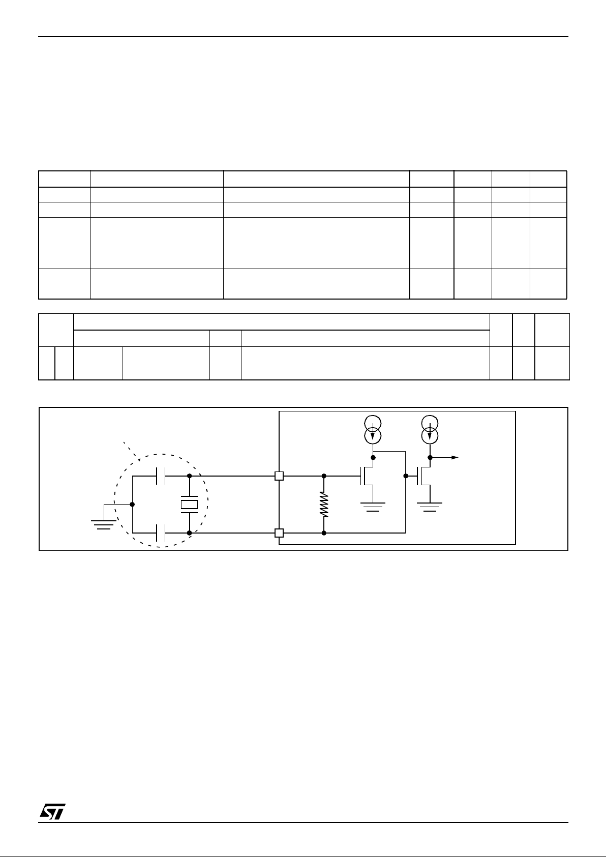
ST7SCR
81/102
CLOCK AND TIMING CHARACTERISTICS (Cont’d)
14.4.3 Crystal Resonator Oscillators
The ST7 internal clock is supplied with one Crystal
resonator oscillator. All the information given in
this paragraph are ba sed on characterization results with specified typical external componants. In
the application, the resonator and the load capaci-
tors have to be placed as cl os e as possible to t he
oscillator pins in order to minimize output distortion
and start-up stabilization time. Refer to the crystal
resonator manufacturer for more details (frequency, package, accuracy...).
Figure 39. Typical Application with a Crystal Resonator
Notes:
1. Resonator characteristics given by the crystal resonator manufacturer.
2. t
SU(OSC)
is the typical oscillator start-up time measured between VDD=2.8V and the fetch of the first instruction (with a
quick V
DD
ramp-up from 0 to 5V (<50µs).
3. The oscillator selection can be optimized in terms of supply current using an high quality resonator with small R
S
value.
Refer to crystal resonator manufacturer for more details.
Symbol Parameter Conditions Min Typ Max Unit
f
OSC
Oscillator Frequency
3)
MP: Medium power oscillator 4 MHz
R
F
Feedback resistor 20 40 kΩ
C
L1
C
L2
Recommanded load capacitances versus equivalent serial resistance of the crystal
resonator (R
S
)
See Table 4 on page 20 (MP oscillator) 22 56 pF
i
2
OSC2 driving current
V
DD
=5V
V
IN=VSS
(MP oscillator) 110 190
µ
A
Oscil.
Typical Crystal Resonator
C
L1
[pF]
C
L2
[pF]
t
SU(osc)
[ms]
2)
Reference Freq. Characteristic
1)
Crystal
MP JAUCH SS3-400-30-30/30
4MHz
∆
f
OSC
=[±30ppm
25°C
,±30ppm
∆
Ta
]
, Typ. R
S
=60
Ω
33 34 7~10
OSC2
OSC1
f
OSC
C
L1
C
L2
i
2
R
F
ST7XXX
RESONATOR
WHEN RESONATOR WITH
INTEGRATED CAPACITORS
Page 82

ST7SCR
82/102
14.5 MEMORY CHARACTERISTICS
Subject to general operating conditions for V
DD
, f
OSC
, and TA unless otherwise specified.
14.5.1 RAM and Hardware Registers
14.5.2 FLASH Memory
Operating Conditions: f
CPU
= 8 MHz.
Warning: Do not connect 12V to VPP before VDD is powered on, as this may damage the device.
14.6 SMARTCARD SUPPLY SUPERVISOR ELECTRICAL CHARACTERISTICS
(T
A
= 0... +70oC, 4.0 < VDD - VSS < 5.5V unless otherwise specified)
Symbol Parameter Conditions Min Typ Max Unit
V
RM
Data retention mode
1)
HALT mode (or RESET) 2 V
DUAL VOLTAGE FLASH MEMORY
Symbol Parameter Conditions Min Typ Max Unit
f
CPU
Operating Frequency
Read mode 8
MHz
Write / Erase mode,
T
A
=25°C
8
V
PP
Programming Voltage 4.0V <= V
DD
<= 5.5V 11.4 12.6 V
I
PP
VPP Current Write / Erase 30 mA
t
PROG
Byte Programming Time
T
A
=25°C
100 500 µs
t
ERASE
Sector Erasing Time 2 10
sec
Device Erasing Time 5 10
t
VPP
Internal VPP Stabilization Time 10 µs
t
RET
Data Retention T
A
≤
55°C 20 years
N
RW
Write Erase Cycles TA=25°C 100 c ycles
SMARTCARD SUPP LY SUPER VISO R
Symbol Parameter Conditions Min Typ Max Unit
5V regulator output (for IEC7816-3 Class A Cards)
V
CARD
SmartCard Power Supply Voltage 4.6 5.00 5.4 V
I
SC
SmartCard Supply Current 55 mA
I
OVDET
Current Overload Detection 120
1)
mA
t
IDET
Detection time on Current Overload 170
1)
1400
1)
µs
t
OFF
V
CARD
Turn off Time (see Figure 35 on
page 61)
C
LOADmax
≤
4.7uF 750 µs
t
ON
V
CARD
Turn on Time (see Figure 35 on
page 61)
C
LOADmax
≤
4.7uF 150 50 0 µs
I
VDD
VDD supply current See note 100 mA
3V regulator output (for IEC7816-3 Class B Cards)
V
CARD
SmartCard Power Supply Voltage 2.7 3.3 V
I
SC
SmartCard Supply Current 50 mA
I
OVDET
Current Overload Detection 100
1)
mA
t
IDET
Detection time on Current Overload 170
1)
1400
1)
us
t
OFF
V
CARD
Turn off Time (see Figure 35 on
page 61)
C
LOADmax
≤
4.7uF 750 us
Page 83

ST7SCR
83/102
Note 1 : Guaranteed by design.
Note 2 : Data based on characterization results, not tested in production.
Notes: V
DD
= 4.75 V, Card consumption = 55mA, CRDCLK frequency = 4MHz, LED with a 3mA current, USB in recep-
tion mode and CPU in WFI mode.
t
ON
V
CARD
Turn on Time (see Figure 35 on
page 61)
C
LOADmax
≤
4.7uF 150 50 0 µs
1.8V regulator output (for IEC7816-3 Class C Cards)
V
CARD
SmartCard Power Supply Voltage 1.65 1.95 V
I
SC
SmartCard Supply Current 20 mA
I
OVDET
Current Overload Detection 100
1)
mA
t
IDET
Detection time on Current Overload 170
1)
1400
1)
us
t
OFF
V
CARD
Turn off Time (see Figure 35 on
page 61)
C
LOADmax
≤
4.7uF 750 us
t
ON
V
CARD
Turn on Time (see Figure 35 on
page 61)
C
LOADmax
≤
4.7uF 150 50 0 µs
Smartcard CLKPin
V
OL
Output Low Level Voltage I=-50uA - - 0.4
2)
V
V
OH
Output High Level Voltage I=50uA V
CARD
-0.5
2)
-- V
T
OHL
Output H-L Fall Time Cl=30pF - 20 ns
T
OLH
Output L-H Rise Time Cl=30pF - 20 ns
F
VAR
Frequency variation - 1 %
F
DUTY
Duty cycle 45 55 %
I
SGND
Short-circuit to Ground 15 mA
Smartcard I/O Pin
V
IL
Input Low Level Voltage - - 0.5
2)
V
V
IH
Input High Level Voltage 0.6V
CARD
2)
-- V
V
OL
Output Low Level Voltage I=-0.5mA - - 0.4
2)
V
V
OH
Output High Level Voltage I=20uA 0.8V
CARD
2)
-V
CARD
2)
V
I
L
Input Leakage Current VSS<VIN<V
SC_PWR
-10 - 10
µ
A
I
RPU
Pull-up Equivalent Resistance VIN=V
SS
24 30 K
Ω
T
OHL
Output H-L Fall Time Cl=30pF - 0.8 us
T
OLH
Output L-H Rise Time Cl=30pF - 0.8 us
I
SGND
Short-circuit to Ground 15 mA
Smartcard RST C4 and C8 Pin
V
OL
Output Low Level Voltage I=-0.5mA - - 0.4
2)
V
V
OH
Output High Level Voltage I=20uA V
CARD
-0.5
2)
- V
CARD
2)
V
T
OHL
Output H-L Fall Time Cl=30pF - 0.8 us
T
OLH
Output L-H Rise Time Cl=30pF - 0.8 us
I
SGND
Short-circuit to Ground 15 mA
SMARTCARD SUPP LY SUPER VISO R
Symbol Parameter Conditions Min Typ Max Unit
Page 84

ST7SCR
84/102
14.7 EMC CHARACTERISTICS
Susceptibility tests are performed on a sample basis during product characterization.
14.7.1 Functional EMS
(Electro Magnetic Susceptibility)
Based on a simple running application on the
product (toggling 2 LEDs through I/O ports), the
product is stressed by two electro magnetic events
until a failure occurs (indicated by the LEDs).
■ ESD: Electro-Static Discharge (positive and
negative) is applied on all pins of the device until
a functional disturbance occurs. This test
conforms with the IEC 1000-4-2 standard.
■ FTB: A Burst of Fast Transient voltage (positive
and negative) is applied to V
DD
and VSS through
a 100pF capacitor, until a functional disturbance
occurs. This test conforms with the IEC 1000-44 standard.
A device reset allows normal operations to be resumed.
Notes:
1. Data based on characterization results, not tested in production.
Symbol Parameter Conditions Neg
1)
Pos
1)
Unit
V
FESD
Voltage limits to be applied on any I/O pin
to induce a functional disturbance
V
DD
=
5V, T
A
=
+25°C, f
OSC
=
8MHz
conforms to IEC 1000-4-2
1 0.7
kV
V
FFTB
Fast transient voltage burst limits to be applied through 100pF on V
DD
and V
DD
pins
to induce a functional disturbance
V
DD
=
5V, T
A
=
+25°C, f
OSC
=
8MHz
conforms to IEC 1000-4-4
22
Page 85

ST7SCR
85/102
EMC CHARACTERISTICS (Cont’d)
14.7.2 Absolute Electrical Sensitivity
Based on three different tests (ESD, LU and DLU)
using specific measurement methods, the product
is stressed in order to determine its performance in
terms of electrical sensitivity. For more details, refer to the AN1181 ST7 application note.
14.7.2.1 Electro-Static Discharge (ESD)
Electro-Static Discharges (1 positive then 1 negative pulse separated by 1 second) are applied to
the pins of each sample according to each pin
combination. The sample size depends of the
number of supply pins of the device (3 parts*(n+1)
supply pin). The Human Body Model is sim ulated.
This test conforms to the JESD22-A114A standard. See Figure 40 and the following test sequences.
Huma n B ody Model Test Sequence
– C
L
is loaded through S1 by the HV pulse gener-
ator.
– S1 switches position from generator to R.
– A discharge from C
L
through R (body resistance)
to the ST7 occurs.
– S2 must be closed 10 to 100ms after the pulse
delivery period to ensure the ST7 is not left in
charge state. S2 must be opened at least 10ms
prior to the delivery of the next pulse.
14.7.2.2 Designing ha rden ed softwar e to av oid
noise problems
EMC characterization and optimization are performed at compon ent level with a typical application environment an d simplified MCU software. It
should be noted that good EMC performance is
highly dependent on the user application and the
software in particular.
Therefore it is recommended that the user applies
EMC software optimization and prequalification
tests in relation with the EMC level requested for
his application.
Software recommendations:
The software flowchart must include the management of runaway conditions such as:
– Corrupted program count er
– Unexpec ted reset
– Critical Data corruption (control registers...)
Prequalification trials:
Most of the common failures (unexpected reset
and program counter corruption) can be reproduced by manually forcing a low state on the RE SET pin or the Oscillator pins for 1 second.
To complete these trials, E SD stress can be applied directly on the device,over the range of specification values.When unexpected behaviour is detected,the sofware can be hardened to prevent unrecoverable errors occurring (see application note
AN1015).
Absolute Maximum Ratings
Figure 40. Typical Equivalent ESD Circuits
Notes:
1. Data based on characterization results, not tested in production.
Symbol Ratings Conditions Maximum value
1)
Unit
V
ESD(HBM)
Electro-static discharge voltage
(Human Body Model)
T
A
=
+25°C
1500 V
ST7
S2
R=1500
Ω
S1
HIGH VOLTAGE
C
L
=
100pF
PULSE
GENERATOR
HUMAN BODY MODEL
Page 86

ST7SCR
86/102
EMC CHARACTERISTICS (Cont’d)
14.7.2.3 Static and Dynamic Latch-Up
■ LU: 3 complementary static tests are required
on 10 parts to assess the latch-up performance.
A supply overvoltage (applied to each power
supply pin), a current injection (applied to e ach
input, output and configurable I/O pin) and a
power supply switch sequence are performed
on each sample. This test confo rms to the EIA/
JESD 78 IC latch-up standard. For more details,
refer to the AN1181 ST7 application note.
■ DLU: Electro-Static Discharges (one positive
then one negative test) are applied to each pin
of 3 samples when the micro is running to
assess the latch-up performance in dynamic
mode. Power supplies are set to the typical
values, the oscillator is connected as near as
possible to the pins of the micro and the
component is put in reset mode. This test
conforms to the IEC1000-4-2 and SAEJ1752/3
standards and is described in Figure 41. For
more details, refer to the AN1181 ST7
application note.
Electrical Sensitivities
Figure 41. S imp lif ie d Diag ram of the ESD Gen erat o r for D LU
Notes:
1. Class description: A Class is an STMicroelectronics internal specification. All its limits are higher than the JEDEC specifications, that m ean s whe n a devic e bel ongs to C lass A it e xceed s the JED EC s tanda rd. B Cla ss str ictly c overs all t he
JEDEC criteria (international standard).
2. Schaffner NSG435 with a pointed test finger.
Symbol Parameter Conditions Class
1)
LU Static latch- up class T
A
=
+25°C A
DLU Dynamic latch-up class
V
DD
=
5.5V, f
OSC
=
4MHz, T
A
=
+25°C
A
RCH=50M
Ω
RD=330
Ω
C
S
=
150pF
ESD
HV RELAY
DISCHARGE TIP
DISCHARGE
RETURNCONNECTION
GENERATOR
2)
ST7
V
DD
V
SS
Page 87

ST7SCR
87/102
EMC CHARACTERISTICS (Cont’d)
14.7.3 ESD Pin Protection Strategy
To protect an integrated circuit against ElectroStatic Discharge the stress must be controlled to
prevent degradation or destruction of the circuit elements. The stress generally affects the circuit elements which are c onnected to t he pads but can
also affect the internal devices when the supply
pads receive the stress. The elements to be protected must n ot re ceive excessive current, vo lt a ge
or heating within their structure.
An ESD network combines the different input and
output ESD protections. This network works, by allowing safe discharge paths for the pins subjected
to ESD stress. Two critical ESD stress cases are
presented in Figure 42 and Figure 43 for standard
pins.
Standard Pin Protection
To protect the output structure the following elements are added:
– A diode to V
DD
(3a) and a diode from VSS (3b)
– A protection device between V
DD
and VSS (4)
To protect the input structure the following elements are added:
– A resistor in series with the pad (1)
– A diode to V
DD
(2a) and a diode from VSS (2b)
– A protection device between V
DD
and VSS (4)
Figure 42. Positive Stress on a Standard Pad vs. V
SS
Figure 43. Negative Stress on a Standard Pad vs. V
DD
IN
V
DD
V
SS
(1)
(2a)
(2b)
(4)
OUT
V
DD
V
SS
(3a)
(3b)
Main path
Path to avoid
IN
V
DD
V
SS
(1)
(2a)
(2b)
(4)
OUT
V
DD
V
SS
(3a)
(3b)
Main path
Page 88

ST7SCR
88/102
EMC CHARACTERISTICS (Cont’d)
Multisupply Configuration
When several types of ground (V
SS
, V
SSA
, ...) and
power supply (V
DD
, V
DDA
, ...) are available for any
reason (better noise immunity...), the structure
shown in Figure 44 is implemented to protect the
device against ESD.
Figure 44. Multisupply Configuration
V
DDA
V
SSA
V
DDA
V
DD
V
SS
BACK TO BACK DIODE
BETWEEN GROUNDS
V
SSA
Page 89

ST7SCR
89/102
14.8 COMMUNICATION INTERFACE CHARACTERISTICS
14.8.1 USB - Universal Bus Interface
Note 1: RL is the load connected on the USB drivers.
Note 2: All the voltages are measured from the local ground potential.
Figure 45. USB: Data Signal Rise and Fall Time
Note1: Measured from 10% to 90% of the data signal. For more detailed informations, plea se refer to
Chapter 7 (Electrical) of the USB specification (version 1.1).
USB DC Electrical Characteristics
Parameter Symbol Conditions Min. Max. Unit
Input Levels:
Differential Input Sensitivity VDI I(D+, D-) 0.2 V
Differential Common Mode Range VCM Includes VDI range 0.8 2.5 V
Single Ended Receiver Threshold VSE 1.3 2.0 V
Output Levels
Static Output Low VOL RL of 1.5K ohms to 3.6v 0.3 V
Static Output High VOH RL of 15K ohm to V
SS
2.8 3.6 V
USBVCC: voltage level USBV V
DD
=5v 3.00 3.60 V
USB: Full speed electrical characteristics
Parameter Symbol Conditions Min Max Unit
Driver characteristics:
Rise time tr Note 1,CL=50 pF 4 20 ns
Fall Time tf Note 1, CL=50 pF 4 20 ns
Rise/ Fall Time matching trfm tr/tf 90 110 %
Output signal Crossover
Voltage
VCRS 1.3 2.0 V
Differentia l
Data Li nes
V
SS
tf
tr
Crossover
points
VCRS
Page 90

ST7SCR
90/102
15 PACKAGE CHARACTERISTICS
15.1 PACKAGE MECHANICAL DATA
Figure 46. 64-Pin Thin Quad Flat Package
Figure 47. 24-Pin Plastic Small Outline Package, 300-mil Width
Dim.
mm inches
Min Typ Max Min Typ Max
A 1.60 0.063
A1 0.05 0.15 0.002 0.006
A2 1.35 1.40 1.45 0.053 0.055 0.057
b 0.30 0.37 0.45 0.012 0.015 0.018
c 0.09 0.20 0.004 0.008
D 16.00 0.630
D1 14.00 0.551
E 16.00 0.630
E1 14.00 0.551
e 0.80 0.031
θ
0° 3.5° 7° 0° 3.5° 7°
L 0.45 0.60 0.75 0.018 0.024 0.030
L1 1.00 0.039
Number of Pins
N 64
c
h
L
L1
e
b
A
A1
A2
E
E1
D
D1
Dim.
mm inches
Min Typ Max Min Typ Max
A 2.35 2.65 0.093 0.104
A1 0.10 0.30 0.004 0.012
B 0.33 0.51 0.013 0.020
C 0.23 0.32 0.009 0.013
D 15.20 15.60 0.599 0.614
E 7.40 7.60 0.291 0.299
e 1.27 0.050
H 10.00 10.65 0.394 0.419
h 0.25 0.75 0.010 0.030
α
0° 8° 0° 8°
L 0.40 1.27 0.016 0.050
Number of Pins
N 24
Dim.
mm inches
Min Typ Max Min Typ Max
C
h x 45×
L
a
A
A1
e
B
D
H
E
Page 91

ST7SCR
91/102
Figure 48. PACKAGE MECHANICAL DATA (Cont’d)
Figure 49. Recommended Reflow Oven Profile (MID JEDEC)
250
200
150
100
50
0
100 200
300 400
Time [sec]
Temp. [° C ]
ramp up
2°C/sec for 50sec
90 sec at 125°C
150 se c above 183°C
ramp down natural
2°C/sec max
Tmax=220+/-5°C
for 25 sec
Page 92

ST7SCR
92/102
16 DEVI CE CONFIGURATIO N AND ORDERING INFORMAT ION
Each device is available for production in ROM
versions and in user programmable versions (High
Density FLASH).
FLASH devices are shippe d to customers with a
default content (FFh).
This implies that FLASH d evices have to be configured by the customer using the Option Byte
while the ROM devices are factory-configured.
16.0.1 Option Bytes
The 8 option bits from the flash a re programmed
through the static option byte SOB1. The description of each of these 8 bits is given below.
Static option Byte (SOB1)
OPT7:6 = Reserved
OPT5= WDGSW
Hardware or software watchdog
This option bit selects the watchdog type.
0: Hardware (watchdog always activated)
1: Software (watchdog to be activated by software)
OPT4 = NEST
Interrupt Controller
This bit enables the nested Interrupt Controller.
0: Nested interrupt controller disabled
1: Nested interrupt controller enabled
OPT3 = ISOCLK
Clock source selecti on
0: Card clock is generated by the divider (48MHz/
12 = 4MHz).
1: Card clock is generated by the oscillator.
OPT2 = RETRY
Number of Retries for UART ISO
0: In case of an erroneous transfer, character is
transmitted 4 times.
1: In case of an erroneous transfer, character is
transmitted 5 times.
OPT1 =
Reserved, must be kept at 1.
OPT0 = FMP_R
Flash memory read-out protec-
tion
This option indicates if the user flash memory is
protected against read-out piracy. This protec tion
is based on read and a write protection of the
memory in test modes and ICP mode. Erasing the
option bytes when the FMP_R option i s selected
induce the whole user memory erasing first.
0 : read-out protection enabled
1 : read-out protection disabled
OPT
7654321
OPT
0
-- --
WDG-
SW
NEST ISOCLK RETRY - FMP_R
Page 93
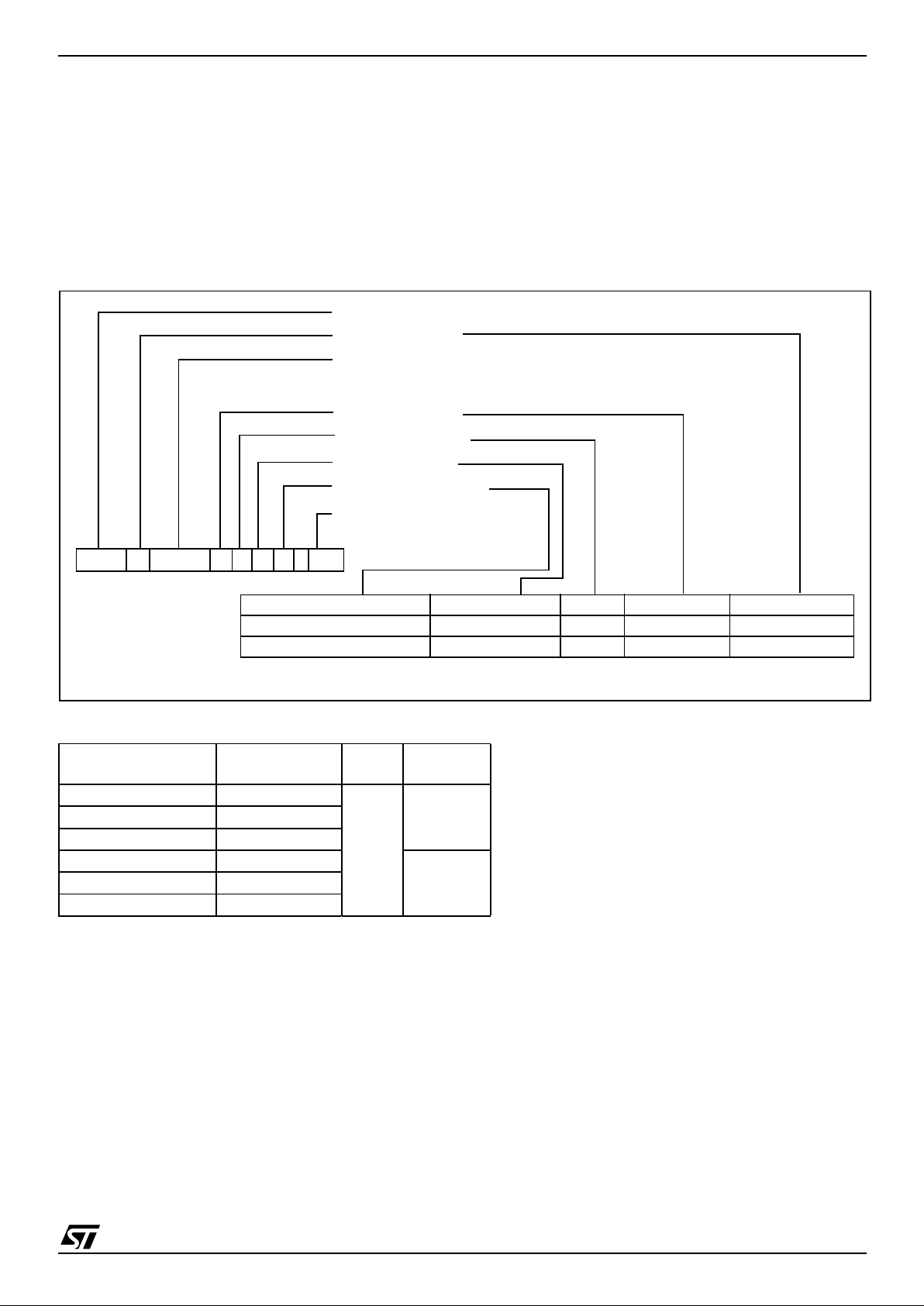
ST7SCR
93/102
16.1 DEVICE ORDERING INFORMATION AND TRANSFER OF CUSTOMER CODE
Customer code is made up of t he ROM contents
and the list of the selected options (if any). The
ROM contents are to be sent on diskette, or by
electronic means, with the hexadecimal file in .S19
format generated b y the development tool . All unused bytes must be set to FFh.
The selected options are communicated to STMicroelectronics using th e correctly completed OPTION LIST appended. See page 94.
The STMicroelectronics Sales Organization will be
pleased to provide detailed information on contractual points.
Figure 50. Sales Type Coding Rules
Table 23. Ordering Information
Note 1. /xxx stands for the ROM or FASTROM-
code name assigned by STMicroelectronics.
ST7 FSCR1 R4B1/xxx
Family
Version Code
Sub family
Number of pins
ROM Size Code
Package Type
Temperature Code
ROM Code (three letters)
1 = Standard (0 to +70°C) T = TQFP 4 = 16K R = 64 pins No letter = ROM
M = Plastic SO x = 24pins F = Flash
P = FASTROM
Sales Type
1)
Program
Memory (bytes)
RAM
(bytes)
Package
ST7SCR1R4T1/xxx 16K ROM
768
TQFP64ST7PSCR1R4T1/xxx 16K FASTROM
ST7FSCR1R4T1 16K Flash
ST7SCR1E4M1/xxx 16K ROM
SO24ST7PSCR1E4M1/xxx 16K FASTROM
ST7FSCR1E4M1 16K Flash
Page 94

ST7SCR
94/102
ST7SCR MICROCONTROLLER OPTION LIST
Customer: . . . . . . . . . . . . . . . . . . . . . . . . . . . .
Address: . . . . . . . . . . . . . . . . . . . . . . . . . . . .
. . . . . . . . . . . . . . . . . . . . . . . . . . . .
Contact: . . . . . . . . . . . . . . . . . . . . . . . . . . . .
Phone No: . . . . . . . . . . . . . . . . . . . . . . . . . . . .
Reference/ROM Code* : . . . . . . . . . . . . . . . . . .
*The ROM code name is assigne d by STMicroelect ronics.
ROM code must be sent in .S19 format. .Hex extension cannot be processed.
Device Type/Memory Size/Package (ch eck only one option):
Conditioning (check only one option):
Note: Die product only for ROM device
Special Marking: [ ] No [ ] Yes "_ _ _ _ _ _ _ _ _ _ "
Authorized characters are letters, digits, ’.’, ’-’, ’/’ and spaces only.
Maximum character count:
S024 (13 char. max) : _ _ _ _ _ _ _ _ TQFP64 (10 char. max) : _ _ _ _ _ _ _ _ _ _
Watchdo g: WDGSW [ ] Software Activation
[ ] Hardware Activation
Nested Interrupts NEST [ ] Nested Interrupts
[ ] Non Nested Interrupts
ISO Clock Sour ce ISOCLK [ ] Oscillator
[ ] Divider
No. of Retries RETRY [ ] 5
[ ] 4
Readout Protection: FMP_R [ ] Disabled
[ ] Enabled
Signature
Date
--------------------------
ROM Device:
--------------------------
|
|
-----------------------------------16K
------------------------------------
|
|
SO24: | [ ] ST7SCR1E4M1
|
TQFP64: | [ ] ST 7S CR1R4T 1
|
--------------------------
FASTROM Device:
--------------------------
|
|
-----------------------------------16K
------------------------------------
|
|
SO24: | [ ] ST7PSCR1E4M1
|
TQFP64: | [ ] ST7PSCR1R4T 1
|
-----------------------------------------------------------------
Packaged Product:
-----------------------------------------------------------------
|
|
----------------------------------------------------
Die Product (dice tested at 25°C only)
----------------------------------------------------
[ ] Tape & Reel [ ] Tray (TQFP package only) | [ ] Tape & Reel
[ ] Tube (SO package only) | [ ] Inked wafer
| [ ] Sawn wafer on sticky foil
Page 95

ST7SCR
95/102
16.2 DEVEL OP MEN T TOOLS
Table 24. Development Tools
16.2.1 ADAPTOR/SOCKET PROPOSAL
TBD
Development Tool Sales Type Remarks
Emulator ST7MDTS1-EMU2B
Programming Board ST7MDTS1-EPB2
Page 96

ST7SCR
96/102
16.3 ST7 APPLICATION NOTES
IDENTIFICATION DESCRIPTION
EXAMPLE DRIVERS
AN 969 SCI COMMUNICATION BETWEEN ST7 AND PC
AN 970 SPI COMMUNICATION BETWEEN ST7 AND EEPROM
AN 971 I²C COMMUNICATING BETWEEN ST7 AND M24CXX EEPROM
AN 972 ST7 SOFTWARE SPI MASTER COMMUNICATION
AN 973 SCI SOFTWARE COMMUNICATION WITH A PC USING ST72251 16-BIT TIMER
AN 974 REAL TIME CLOCK WITH ST7 TIMER OUTPUT COMPARE
AN 976 DRIVING A BUZZER THROUGH ST7 TIMER PWM FUNCTION
AN 979 DRIVING AN ANALOG KEYBOARD WITH THE ST7 ADC
AN 980 ST7 KEYPAD DECODING TECHNIQUES, IMPLEMENTING WAKE-UP ON KEYSTROKE
AN1017 USING THE ST7 UNIVERSAL SERIAL BUS MICROCONTROLLER
AN1041 USING ST7 PWM SIGNAL TO GENERATE ANALOG OUTPUT (SINUSOID)
AN1042 ST7 ROUTINE FOR I²C SLAVE MODE MANAGEMENT
AN1044 MULTIPLE INTERRUPT SOURCES MANAGEMENT FOR ST7 MCUS
AN1045 ST7 S/W IMPLEMENTATION OF I²C BUS MASTER
AN1046 UART EMULATION SOFTWARE
AN1047 MANAGING RECEPTION ERRORS WITH THE ST7 SCI PERIPHERALS
AN1048 ST7 SOFTWARE LCD DRIVER
AN1078 PWM DUTY CYCLE SWITCH IMPLEMENTING TRUE 0% & 100% DUTY CYCLE
AN1082 DESCRIPTION OF THE ST72141 MOTOR CONTROL PERIPHERAL REGISTERS
AN1083 ST72141 BLDC MOTOR CONTROL SOFTWARE AND FLOWCHART EXAMPLE
AN1105 ST7 PCAN PERIPHERAL DRIVER
AN1129 PERMANENT MAGNET DC MOTOR DRIVE.
AN1130
AN INTRODUCTION TO SENSORLESS BRUSHLESS DC MOTOR DRIVE APPLICATIONS
WITH THE ST72141
AN1148 USING THE ST7263 FOR DESIGNING A USB MOUSE
AN1149 HANDLING SUSPEND MODE ON A USB MOUSE
AN1180 USING THE ST7263 KIT TO IMPLEMENT A USB GAME PAD
AN1276 BLDC MOTOR START ROUTINE FOR THE ST72141 MICROCONTROLLER
AN1321 USING THE ST72141 MOTOR CONTROL MCU IN SENSOR MODE
AN1325 USING THE ST7 USB LOW-SPEED FIRMWARE V4.X
AN1445 USING THE ST7 SPI TO EMULATE A 16-BIT SLAVE
AN1475 DEVELOPING AN ST7265X MASS STORAGE APPLICATION
AN1504 STARTING A PWM SIGNAL DIRECTLY AT HIGH LEVEL USING THE ST7 16-BIT TIMER
PRODUCT EVALUATION
AN 910 PERFORMANCE BENCHMARKING
AN 990 ST7 BENEFITS VERSUS INDUSTRY STANDARD
AN1077 OVERVIEW OF ENHANCED CAN CONTROLLERS FOR ST7 AND ST9 MCUS
AN1086 U435 CAN-DO SOLUTIONS FOR CAR MULTIPLEXING
AN1150 BENCHMARK ST72 VS PC16
AN1151 PERFORMANCE COMPARISON BETWEEN ST72254 & PC16F876
AN1278 LIN (LOCAL INTERCONNECT NETWORK) SOLUTIONS
PRODUCT MIGRATION
AN1131 MIGRATING APPLICATIONS FROM ST72511/311/214/124 TO ST72521/321/324
AN1322 MIGRATING AN APPLICATION FROM ST7263 REV.B TO ST7263B
AN1365 GUIDELINES FOR MIGRATING ST72C254 APPLICATION TO ST72F264
PRODUCT OPTIMIZATION
Page 97

ST7SCR
97/102
AN 982 USING ST7 WITH CERAMIC RESONATOR
AN1014 HOW TO MINIMIZE THE ST7 POWER CONSUMPTION
AN1015 SOFTWARE TECHNIQUES FOR IMPROVING MICROCONTROLLER EMC PERFORMANCE
AN1040 MONITORING THE VBUS SIGNAL FOR USB SELF-POWERED DEVICES
AN1070 ST7 CHECKSUM SELF-CHECKING CAPABILITY
AN1324 CALIBRATING THE RC OSCILLATOR OF THE ST7FLITE0 MCU USING THE MAINS
AN1477 EMULATED DATA EEPROM WITH XFLASH MEMORY
AN1502 EMULATED DATA EEPROM WITH ST7 HDFLASH MEMORY
AN1529 EXTENDING THE CURRENT & VOLTAGE CAPABILITY ON THE ST7265 VDDF SUPPLY
AN1530
ACCURATE TIMEBASE FOR LOW-COST ST7 APPLICATIONS WITH INTERNAL RC OSCIL-
LATOR
PROGRAMMING AND TOOLS
AN 978 KEY FEATURES OF THE STVD7 ST7 VISUAL DEBUG PACKAGE
AN 983 KEY FEATURES OF THE COSMIC ST7 C-COMPILER PACKAGE
AN 985 EXECUTING CODE IN ST7 RAM
AN 986 USING THE INDIRECT ADDRESSING MODE WITH ST7
AN 987 ST7 SERIAL TEST CONTROLLER PROGRAMMING
AN 988 STARTING WITH ST7 ASSEMBLY TOOL CHAIN
AN 989 GETTING STARTED WITH THE ST7 HIWARE C TOOLCHAIN
AN1039 ST7 MATH UTILITY ROUTINES
AN1064 WRITING OPTIMIZED HIWARE C LANGUAGE FOR ST7
AN1071 HALF DUPLEX USB-TO-SERIAL BRIDGE USING THE ST72611 USB MICROCONTROLLER
AN1106 TRANSLATING ASSEMBLY CODE FROM HC05 TO ST7
AN1179
PROGRAMMING ST7 FLASH MICROCONTROLLERS IN REMOTE ISP MODE (IN-SITU PRO-
GRAMMING)
AN1446 USING THE ST72521 EMULATOR TO DEBUG A ST72324 TARGET APPLICATION
AN1478 PORTING AN ST7 PANTA PROJECT TO CODEWARRIOR IDE
AN1527 DEVELOPING A USB SMARTCARD READER WITH ST7SCR
AN1575 ON-BOARD PROGRAMMING METHODS FOR XFLASH AND HDFLASH ST7 MCUS
IDENTIFICATION DESCRIPTION
Page 98

ST7SCR
98/102
17 SUMMARY OF CHANGES
Description of the changes between the current release of the specification and the previous one.
Revision Main changes Date
1.2
Removed LVD option bit (LVD cannot be disabled)
Updated Figure 7 on page 15
Dec-01
1.3
Changed status of the document
Changed Table 1, “Device Summary,” on page 1
Changed Figure 4 on page 10
Changed Section 4.2 on page 14
Added note in Section 4.5 on page 15
Changed description of the following registers in Section 12.3.4 on page 46: EP0R, Endpoint
Transmission Register and Endpoint 2 Reception Register.
Moved “Power Supply Management” chapter to Section 12.4.3.1 on page 56
Updated Section 14 on page 76
Added Section 14.7 on page 84
Changed Figure 46 on page 90
Removed references to true open drain pins
Changed Section 16.1 on page 93
Added warning in Section 14.5.2 on page 82
Added Erratasheet on page 99
March-03
Page 99

Rev. 1.2
March 2003 99/102
ERRATA SHEET
ST7SCR LIMITATIONS AND CORRECTIONS
18 SILICON IDENTIFICATION
This document refers only to ST7FSCR devices shown in Table 25. They are identifiable both
by the last letter of the Trace code marked on the device package and by the last 3 digits of
the Internal Sales Type printed on the box label (see also Figure 51)
Table 25. Device Identification
19 REFERENCE SPECIFICATION
ST7SCR Datasheet 1.3 (March 2003).
20 SILICON LIMITATIONS
20.1 UNEXPECTED RESET FETCH
If an interrupt request occurs while a "POP CC" instruction is executed, the interrupt controller
does not recognise the source of the interrupt and, by default, pa sses the RESE T vector address to the CPU.
To solve this issue, a "POP CC" instruction must always be preceded by a "SIM" instruction.
20.2 USB: TWO CONSEC UTIVE SETUP TOKENS
Description
When tw o c onsec u tive S ETUP t okens are rec eiv ed and t he soft wa re do es n ot have ti me to
write the value 8 in the Endpoint 0 Reception Counter Register (CNT0RXR ), the data associated with the second SETUP are not copied to the buffer.
Impact
The impa ct depen ds on the ho st behavi our. In the USB Spec 2.0 it is sta ted (cha pter 5. 5.5
p43) tha t: “A S etu p tra nsac tion sh oul d n ot no rma lly b e s ent bef ore th e co mp letion o f a previous control transfer. However, if a transfer is aborted, for example, due to err ors on the bus,
the host can send the next Setup transaction prematurely from the endpoint’s perspective”. If
the new Setup token is sent because an error occurs in the pr evious one, it should contain the
same data so no application malfunction will occur.
Trace Code marked on device Internal Sales Type on box label
Flash Devices: “xxxxxxxxxX”
7FSCRxxxx$M1
7FSCRxxxx$T1
Page 100

ERRATA SHEET
100/102
This limitation will be corrected i n the nex t si licon revision. In the new revision, when a SETUP
token is received, the value loaded in the internal counter is fixed to 8 by hardware independently of the value in the CNT0RXR register.
20.3 USB BUFFER SHARED MEMORY ACCES S
Description
When f
CPU
is at 4 MHz, a value w ritten in the U SB buffer may be corrupted when VDD is less
than 4.4V. This limitation will be corrected in the next silicon revision.
Impact
USB buffer access cannot be guaranteed over the full V
DD
range when f
CPU
is at 4 MHz.
20.4 WDG (WATCHDOG) LIMITATIONS
In flas h de vice s, th e WD G pre sca ler value is no t 65 536 as de scri bed i n Section 12.1.3 on
page 40 (Figure 25), it is actually 16.
This will be corrected in the next revision of the silicon.
20.5 SUPPLY CURRENT IN HALT MODE (SUSPEND) LIMITATIONS
The current consumption (I
DD
) in some devices may exceed th e maximum specified in the
documentation (up to 1mA).
Workaround
Declare 200mA max. power value in the USB Configuration Descriptor.
20.5.1 V
PP
Pin Limitation
In the impacted flash dev ices, c ontrary to the datas heet spec ification ( which specifies t hat it
must be tied to V
SS
), the VPP pin must be tied to VDD in operating mode. This will be fixed in
the next silicon revision .
20.6 START-UP
The ST7SCR relies on internal LVD and it may not start-up correctly if t he power supply is
slow.
Workaround
Put a 1MΩ resistor between V
DD
and V
SS
to eliminate the offset on VDD that may cause this
power-on problem.
 Loading...