

Page 1
USB 1.1 HUB WITH 2 DOWNSTREAMS, FULL SPEED
FUNCTION, 8-BIT MCU, 10-BIT ADC, 3 TIMERS, 2 PWMs
■ Memories
– 32K High Density Flash (HD-Flash) program
memory with read/write protection or 16K
ROM
– In-Application Programming (IAP) via USB
and In-Circuit programming (ICP) for Flash
device
– 768 bytes RAM memory including up to 176
bytes for USB buffers and up to 256 bytes
stack
■ Clock, Res et and Supp ly M ana g e m ent
– Enhanced Reset System (Power On Reset)
and Low Voltage Detector (LVD) on some devices
– PLL for generating 48 MHz USB clock using a
4 MHz crystal
– Up to 12 MHz internal frequency on ROM de-
vice
– Up to 8 M Hz i nternal frequ ency on Flash de-
vice
– Clock-out capability
– 2 Power saving modes
■ USB HUB Function
– 3 bus-powered downstream ports (1 connect-
ed internally to embedded function)
– Individual downs trea m Power Swit c hing
– Overcurrent Protection for each downstream
– Supports all USB Standard and HUB com-
mands
– Integrated 3.3V voltage regulator and trans-
ceivers
■
USB Full Speed Function
– 7 USB Endpoints:
One 8-byte Bidirectional Control Endpoint
One 64-byte In Endpoint (Interrupt or Bulk)
One 64-byte Out Endpoint (Interrupt or Bulk)
Four 8-byte In Endpoints (Interrupt)
– DMA for Full speed applications compliant
with USB specification (v 2.0)
– Suspend and Resume operations
■ 35 I/ O Ports
– 35 multifunctional bidirectional I/O lines
– 23 individually selectable external interrupts
(3 vectors) with per port programmable sensi-
tivity
– Pull up resistors in input individually selecta-
ble by software
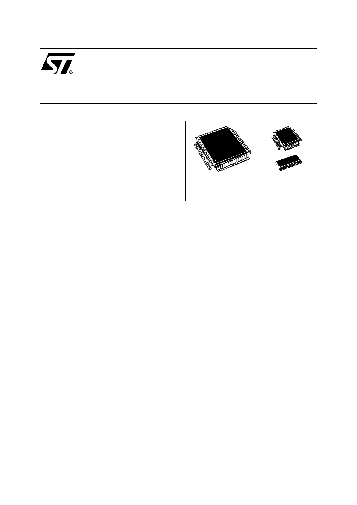
ST7HUB
DATA BRIEFING
TQFP64
10x10
– 3 ports (20 I/Os) can be individually config-
ured to open drain pull up configuration for
PS/2 and keyboard function.
– 7 high sink outputs (8 mA@0.4 V/
20 mA@1.3 V)
■ 3 Timers
– Configurable watchdog timer (8 to 500 ms
timeout)
– 8 bit Time Base Unit (TBU) for generating pe-
riodic interrupts, cascadable with ART
– 8 bit Auto-Reload Timer (ART) with 2 Input
Captures, 2 PWM outputs and External Clock
Input
■ Analog Peripheral
– 10-bit A/D Converter with
ence pins
4 high impedance high accuracy channels
12 standard channels
■ 1 Communication Interface
– Serial Peripheral Interface (SPI)
■ Instruction Set
– 8-bit data manipulation
– 63 basic instructions
– 17 main addressing modes
– Nested Interrupts
– 8 x 8 unsigned multiply instruction
– True bit manipulation
■ Development Tools
– Full hardware/software development package
■ Operating Conditions
– 4.0 to 5.25V power supply
– 0 to 70°C temperature range
Subsets in
TQFP44 10x10
and SO34
V
and V
REF+
REF-
refer-
Rev. 1.0
October 2001 1/6
This is preliminary information on a new product now in development. Details are subject to change without notice.
1
Page 2

ST7HUB
1 INTRODUCTION
The ST7HUB is a USB microcontroller based on
ST7 core, which is an enhanced industry-standard
architecture. The USB module of the ST7HUB is a
compound device, consisting of a 3-port HUB an d
an attached embedded function. To the USB host,
the embedded function appears as an attached
port of the HUB with its own device address an d
endpoints.
In addition to the peripherals for USB full speed
data transfer and to the HUB, the ST7HUB includes all the necessary features for a gaming peripheral or a multimedia keyboard application.
– 10-bit Analog-to-Digital converter (ADC) with 16
multiplexed analog inputs and external references. 4 of the channels have optimized layout so
that external source can have up to 50kΩ impedance
– 8-bit Auto-Reload Timer with 2 input capture
functions, 2 PWM outputs and external clock in-
put
– Serial Peripheral Interface
– Low voltage reset ensuring proper power-on or
power-off of the device (selectable by option)
– Digital Watchdog
The ST72FHUB devices are the Flash version s of
the ST7HUB in a TQFP64 10x10 package.
The ST7HUB devices are the ROM versions in a
TQFP64 10x10 package.
The device is also available in TQFP44 and SO34
packages without HUB function.
2/6
Page 3

INTRODUCTION (Cont’d)
Figure 1. General Block D iagram
ST7HUB
V
V
RESET
OSCIN
OSCOUT
DD
SS
LVD
POWER
SUPPLY
CONTROL
8-BIT CORE
ALU
WATCHDOG
FLASH (32KB)
ROM (16KB)
OSCILLATOR
PLL
RAM
(512 Bytes)
USB RAM
(256 Bytes)
USB DMA
1 CRTL
1 BULK / INT IN
1 BUL K / INT O U T
4 INT IN
Internal
CLOCK
USB SIE
PORT D
8BIT ARTIMER
2 INPUT CAPT
2 OUTPUT COMP
2PWM
PORT E
SPI
PORT B
ADDRESS AND DATA BUS
10 BIT ADC
4 HIGH IMPED.
CHANNELS
12 STD CH
EXT. REF.
PORT A
PORT C
HUB POWER
LOGIC
HUB
CONTROLLER
PD6:0
(7 bits)
PE7:0
(8 bits)
PB3:0
(4 bits)
V
REF+
V
REF-
High Impedance ADC
(4 channels )
V
DDA
V
SSA
PA7:0
(8 bits)
PC7:0
(8 bits)
USBDP2
USBV
CC2
USBDM2
USBDP3
USBV
CC3
USBDM3
XVR
XVR
PORT 2
LOGIC
PORT 3
LOGIC
HUB BLOCK
PORT 1
LOGIC
USB SIE
HUB REPEATER
FRAME TIMER
XVR
USBDP0
USBV
CC0
USBDM0
USBV
DD
USBV
SS
3/6
1
Page 4

ST7HUB
2 PIN DESCRI PTION
Figure 2. 64-Pin TQFP Package Pinout
USBDM2
USBV
CC2
USBDP2
USBV
SS
USBDM0
USBV
CC0
USBDP0
USBV
DD
USBDM3
USBV
CC3
USBDP3
V
SS2
OSCOUT
OSCIN
V
DD2
RESET
REF-VREF+
AIN13
AIN12
V
AIN11
AIN10
PB1 / AIN9
PB3 / AIN15
PB2 / AIN14
64 63 62 61 60 59 58 57 56 55 54 53 52 51 50 49
1
2
3
4
5
6
7
8
9
10
11
12
13
14
15
16
Ext Int 0
17 18 19 20 21 22 23 24 29 30 31 32
PC1
PC2
PC0 / MCO
PC3 / LPWR
PC4 / PWRON2
PC5 / OVCUR2
PC6 / OVCUR3
PB0 / AIN8
Ext Int 1
25 26 27 28
PD0 (HS)
PD1 (HS)
PC7 / PWRON3
PA7 / AIN7
PD2 (HS)
PA6/ AIN6
PD3 (HS)
SSAVSS1VDDAVDD1
V
Ext Int 2
Ext Int 2
Ext Int 1
SS3
DD3
V
V
PA5 / AIN5
48
PA4 / AIN4
47
PA3 / AIN3
46
PA2 / AIN2
45
PA1 / AIN1
44
PA0 / AIN0
43
PE7 / ARTIC2 / ICCCLK
42
PE6 / ARTIC1/ ICCDATA
41
PE5 / PWM2
40
PE4 / PWM1
39
V
38
PP
PE3 / SCLK
37
36
PE2 / SS
35
PE1 / MISO
34
PE0 / MOSI
33
PD6 (HS)
PD5 (HS)
4/6
1
ARTCLK / PD4 (HS)
Page 5

Figure 3. 44-pin TQFP and 34-pin SO Package Pinou t
ST7HUB
USBV
PB3 / AIN15
USBV
USBDM0
USBDP0
CC0
USBDP0
USBV
DD
V
SS2
OSCOUT
OSCIN
V
DD2
RESET
PA1 / AIN1
PA2 / AIN2
PA3 / AIN3
PA4 / AIN4
PA5 / AIN5
USBV
USBDM0
USBV
USBDP0
REF-VREF+
AIN13
AIN12
PC1
PC2
V
PD0 (HS)
PD1 (HS)
PB2 / AIN14
44 43 42 41 40 39 38 37 36 35 34
1
2
SS
3
4
5
6
7
8
9
10
Ext Int 0 Ext Int 1
11
12 13 14 15 16 17 18 19 20 21 22
PC0 / MCO
1
2
3
4
5
V
DD1
V
SS1
AIN10
AIN11
V
REF+
V
REF-
AIN12
AIN13
SS
6
7
8
9
10
11
12
13
14
15
CC0
16
17
AIN11
PD2 (HS)
PD3 (HS)
Ext Int 2
Ext Int 1
Ext Int 1
AIN10
PA7 / AIN7 / ICCDATA
Ext Int 2
Ext Int 1
DD3
V
V
PA6/ AIN6 / ICCCLK
SS3
SS1VDD1
V
PA5 / AIN5
33
PA4 / AIN4
32
PA3 / AIN3
31
PA2 / AIN2
30
PA1 / AIN1
29
PA0 / AIN0
28
PE7 / ARTIC2 / ICCCLK
27
PE6 / ARTIC1/ ICCDATA
26
PE5 / PWM2
25
PE4 / PWM1
24
V
23
PP
PD5 (HS)
ARTCLK / PD4
PA0 / AIN0
34
33
PE7 / ARTIC2 / ICCCLK
32
PE6 / ARTIC1 / ICCDATA
31
PE5 / PWM2
30
PE4 / PWM1
29
V
PP
28
PD4 (HS) / ARTCLK
V
27
26
25
24
23
22
21
20
19
18
SS3
V
DD3
PD1 (HS)
PD0 (HS)
RESET
V
DD2
OSCIN
OSCOUT
V
SS2
USBV
DD
5/6
1
Page 6

ST7HUB
Notes:
Information furnished is believed to be accurate and reliable. However, STMicroelectronics assumes no responsibility for the consequences
of use of such information nor for any infringement of patents or other rights of third parties which may result from its use. No license is granted
by implic ation or otherwise under any patent or patent r i ghts of STM i croelectr oni cs. Spec i fications mentione d i n this publication are s ubj ect
to change without notice. This publication supersedes and replaces all information previously supplied. STMicroelectronics product s are not
authorized for use as cri tical comp onents in lif e support devi ces or systems without the express written appr oval of STMic roelectronics.
The ST logo is a registered trademark of STMicroelectronics
2001 STMicroelectronics - All Rights Reserved.
STMicroelectronics Grou p of Companie s
http://www.s t. com
Purchase of I
2
C Components by STMicroelectronics conveys a license under the Philips I2C Patent. Rights to use the se compone nt s i n an
2
C system i s granted pro vi ded that the sy stem conforms to the I2C Standard Specification as defined by Philips.
I
Australi a - Brazil - Canada - China - Fi nl and - Franc e - Germany - Hong Kong - Ind i a - Is rael - Ital y - J apan
Malaysi a - M al ta - Morocco - Singapore - Spain - Sweden - Sw itzerland - Uni t ed Kingdo m - U.S.A.
6/6
1
 Loading...