

Page 1
ST75C530
ST75C540
SUPERINTEGRATED DEVICESWITHDSP,AFE& MEMORIES
FOR TELEPHON Y, MODEM, FA XOVERINTERNET& POTSLINES
SUMMARIZED FEATURES
(fordetailed features,see page 4)
.
SINGLECHIP FAXUp to 14.4Kbps(V.17)
.
FULL DUPLEX DATA MODEM UP TO
14.4Kbps(V.32Bis)
.
DIGITALANSWERING MACHINE :
- 4.8Kbps VOCODER
- VAR IABLEPLAYBACKSPEED(+50%to -50%)
-ADPCM 32, 34, 16KbpsVOCODER
.
FULL-DUPLEX DIGITAL SPEAKERPHONE
WITHECHO CANCELLATION
.
PROGRAMMABLERING DETECTION
.
16 PROGRAMMABLE TONE DETECTORS
FORCLID AND SCWID
.
DTMFDETECTION
.
VERSATILEHOSTINTERFACES
.
16 GENERALPURPOSEI/O PORTS
.
2 RELAYDRIVE OUTPUTS
.
SINGLE5V POWER SUPPLY
.
TYPICALACTIVEPOWERCONSUMPTION:
650mW(ST75C530),750 mW(ST75C540)
.
LOWPOWER MODE < 30mW
.
80-PINTQFPPACKAGE (14mmx 14mm)
DESCRIPTION
ST75C530 and ST75C540 are two super-integrated devices including DSP, Modem and Audio
Analog Front Ends and memories for Telephony,
Modemand FAXapplications.
These devices can be used for classical applicationsover POTSlines or over Internet.
The super integration technology allows a significant cost reduction on bill of materials for equipment like High-End phones, INTERNET phones,
phone-Fax,INTERNET FAX, ...
The devices are used with a host processor
througha Dual Port RAM allowing the use of any
kind of microcontroller(RISC, CISC,General Purpose 8-bitµC, ...).
The embedded software includes :
- handsetwith listeninggroup capability,
- fullduplex handsfree,
- voicecoder/decoderat 4.8Kbpsforstaticanswering machine applications and ADPCM 16Kbps,
24Kbps and 32Kbps for high quality message
recording,
- Tone and DTMF generators,
- Tone and DTMF detectors,
- FAX up to 14.4Kbps,
- Data-Modemup to 14.4Kbps(ST75C540 only).
The DSPsofware is extensively user configurable
allowing specific functions to be supported like
Caller Identifier (CLID) and Second Call Waiting
Identifier(SCWID).
The DSP software includes a transparent mode
allowing the host controller to access directly the
modem Analog Front End and the Audio AFE
through the dual Port RAM.This is very useful for
hostprocessingmodem solutions (orsoft modem)
wherethe modulationandthedemodulation(V.34,
V.90)are done by the applicationmain processor.
In transparentmode, the embedded DSP can be
used simultaneouslywith the same samples.
Thetransparentmode for audioAFEis providedto
play audio filesor to recordvoice and/oraudio.
TQFP80 (14 x14 x 1.4mm)
(Full Thin Plastic Quad Flat Pack)
ORDER CODE : ST75C530FP-A
ST75C540FP-A
February 1999
1/84
Page 2

ST75C530- ST75C540
CONTENTS Page
I DETAILED FEATURES ................................................. 4
II PIN DESCRIPTION .................................................... 5
II.1 PIN CONNECTIONS. . .. ................................................ 5
II.2 HOST INTERFACE. .................................................... 6
II.3 ANALOGINTERFACE . ................................................. 6
II.4 GENERALPURPOSEIO ANDRELAY . . .. ................................. 6
II.5 MISCELLANEOUS. .................................................... 7
II.6 POWER SUPPLY . . . . . . . . . . . . .. . . . .. . . . . . . . . ........................... 7
III BLOCK DIAGRAMS.................................................... 8
III.1 ANALOGINTERFACE . ................................................. 8
III.2 INTERNALBLOCK DIAGRAM . ........................................... 8
IV ELECTRICAL SPECIFICATIONS ......................................... 9
IV.1 MAXIMUMRATINGS................................................... 9
IV.2 RECOMMENDED OPERATINGCONDITIONS. . . . . . . . . ...................... 9
IV.3 DIGITALINTERFACE. . . . . . . . . . . . .. . . . .. . . . ............................. 10
IV.4 MODEMANALOGINTERFACE. . . . ....................................... 11
IV.5 AUDIOANALOG INTERFACE . ........................................... 11
IV.6 AC CHARACTERISTICS . . .. . . . .. . . . . . . . . . . . . . . ......................... 12
V FUNCTIONAL DESCRIPTION............................................ 13
V.1 SYSTEMARCHITECTURE . . . . .......................................... 13
V.2 MODES OF OPERATION. . .. . . . .. . . . . . . . . . . . . . . ......................... 13
V.3 OPERATIONS. . . . . . . . . . . . . . . . . .. . . . . . ................................. 13
V.3.1 ModemTransmitterDescription . . .. ....................................... 13
V.3.2 ModemReceiver Description . . .. . . . .. . . . .. . . .. . . . .. ...................... 13
V.3.3 Tone GeneratorDescription . . . . .......................................... 13
V.3.4 Tone Detector Description . .............................................. 13
V.3.5 V.21 Channel2 FlagDetectorDescription . .................................. 13
V.3.6 HDLC Description . . . . . . . . . . . . .. . . . .. . . . . . . . . ........................... 13
V.3.7 UARTDescription . . . . . . . . . . . . .. . . . .. . . . . . . . . ........................... 13
V.3.8 DTMF Detector Description. .............................................. 13
V.3.9 Ring Detector . . . . . . . . . . . . . . . . . . . . . . . . ................................. 13
V.3.10 VOCODERDescription. ................................................. 14
V.3.11 VoiceActivity Detector(VAD). . . . . . . . . . . . .. . . . . . . . .. ...................... 14
V.3.12 Telephony Functions. . . . ................................................ 15
V.3.13 Low PowerMode . . . . . . . . . . . . . . . . . . . . . . . . . . . ........................... 18
V.3.14 Reset. . . . . . . . .. . . . . .............................................. .... 18
V.4 MODEMINTERFACE. . .. . . . . . . . . . . . . . . . . . . ............................. 18
V.4.1 AnalogInterface . . . . ................................................... 18
V.4.2 GeneralI/O and Relay Interface. . . . ....................................... 18
V.4.3 Crystal. ........................................................... ... 19
V.4.4 TypicalApplicationSchematic. . . . . . . . . . . . . . . . . . . . . . . ...................... 19
V.4.5 Host Interface . . . . . . . . . . . . . . . . . . . . . . . . ................................. 19
VI USER INTERFACE..................................................... 21
VI.1 DUAL PORT RAMDESCRIPTION. ........................................ 21
VI.2 COMMANDSET. . . . ................................................... 25
VI.3 COMMANDSET SHORT FORM . . . . . . . . . . . . .............................. 26
VI.4 STATUS- REPORTS. . . . . . . . . . . . . . . . . . . . . . ............................. 27
VI.5 DATA EXCHANGES. . .. ................................................ 27
2/84
Page 3

ST75C530- ST75C540
VII COMMAND SET DESCRIPTION.......................................... 28
VIII STATUS DESCRIPTION ................................................ 43
VIII.1 COMMANDACKNOWLEDGEAND REPORT. . . . . . .......................... 43
VIII.2 MODEMSTATUS. . .. . . . . . . . . . . . . . . . . . . . . . .. ........................... 44
IX TONE DETECTORS.................................................... 53
IX.1 OVERVIEW. .......................................................... 53
IX.2 DESCRIPTION. ....................................................... 53
IX.3 EXAMPLE. . . . . . . .. . . . .. . . . . . . . . . . .................................... 59
X PARALLELDATA EXCHANGE........................................... 60
X.1 OVERVIEW. .......................................................... 60
X.2 TRANSMITBUFFER . . .. . . . . . . . . . . . . . . . . . . ............................. 60
X.3 RECEIVEBUFFER. .................................................... 61
X.4 INTERRUPTION. . . . ................................................... 61
X.5 DATA FORMAT . . . . ................................................... 61
X.6 FORMCOMMAND . .................................................... 63
XI TRANSMITTING DATAIN PARALLELMODE ............................... 64
XI.1 DESCRIPTION. ....................................................... 64
XI.2 MODEMFLOW CHART . . . . ............................................. 65
XI.3 HOST FLOW CHART. . . . . . . . . . . . . . . . . . . . . . ............................. 65
XI.4 ERROR DETECTION. . .. . . . . . . . . . . . . . . . . . . ............................. 66
XI.5 SYNCHRONOUS MODE . . . . . . . . . . . . . . . . . .. . . . . ......................... 66
XI.6 HDLC MODE. . . . ...................................................... 67
XI.7 UARTMODE DESCRIPTION. . . . . . . .. . . . .. . . .. . . . .. ...................... 69
XII RECEIVINGIN PARALLEL MODE ........................................ 70
XII.1 DESCRIPTION. ....................................................... 70
XII.2 MODEMFLOW CHART . . . . ............................................. 70
XII.3 HOST FLOW CHART. . . . . . . . . . . . . . . . . . . . . . ............................. 70
XII.4 ERROR DETECTION. . .. . . . . . . . . . . . . . . . . . . ............................. 71
XII.5 SYNCHRONOUS MODE . . . . . . . . . . . . . . . . . .. . . . . ......................... 72
XII.6 HDLC MODE. . . . ...................................................... 72
XII.7 UARTMODE. . . . ...................................................... 74
XIII VOCODERDATA EXCHANGE ........................................... 74
XIII.1 OVERVIEW. .......................................................... 74
XIII.2 VOCODERBUFFER. . .. ................................................ 74
XIII.3 TRANSMIT(DECODER) . . . . . . . . . . . . .. . . . .. . . .. ......................... 74
XIII.4 RECEIVE(CODER) . . .. ................................................ 75
XIV TRANSPARENTMODE DATA EXCHANGE................................. 75
XV DEFAULT CALL PROGRESS TONE DETECTORS........................... 76
XVI DEFAULT ANSWER TONEDETECTORS .................................. 76
XVII ELECTRICAL SCHEMATICS............................................. 77
XVIII PCB DESIGN GUIDELINES.............................................. 78
XIX APPENDIX A : MODESOF OPERATION . .................................. 78
XX PACKAGE MECHANICAL DATA ......................................... 83
3/84
Page 4

ST75C530- ST75C540
I - DETAILED FEATURES
SingleChip Fax
- ITU-T V.17, V.29,V.27ter,V.21with Fax support
- V.17, V.29 (T104), V.27ter short trains,
V.33 half-duplex
- V.21 flag detection and 4 tone detection during
high speedreception modes
- V.21 flag detection, DTMF detection and 4
tone detection duringV.21channel2 reception
modes
- Programmable call progress and call waiting
detection
- Parallel data handling
- HDLC and UART framingsupport
- 1700Hz and 1800Hz carrier
- Full implementation of the V.17, V.33, V.29 and
V.27handshakes
- 0 to -15dBmprogrammabletransmitpower
- 0 to-47dBmreceiverdynamicrange(ST75C530)
0 to-45dBmreceiverdynamicrange(ST75C540)
Handset Mode
- Rx and Tx AGC versus line current for line
losses compensation comply with most of
country regulations
- Dynamic limiter in transmit path to prevent
distortion
- Two wayconversationrecording
Hands-freeMode
- Fullduplex speakerphoneusing LMSadaptative
filtering including line echo cancellation and
acoustic echo cancellation
- Rx and Tx AGC versus line current for line
losses compensation comply with most of
country regulations
- Dynamic limiter in transmit path to prevent
distortion
- Loudspeakervolume control
- Two wayconversationrecording
Full Duplex Data Modem
- ITU-T V.32bis, V.32 (14400,12000, 9600, 7200,
4800bps) (*)
- Maximum round trip delay : 1.2s (satellite hops)
(*)
- Up to 10Hzof phaseroll on far end echo (*)
- ITU-T V.22bis,V.22(2400, 1200bps)(*)
- V.32bis/V.32/V.22bis/V.22automode(*)
- ITU- V.23,V.21,bell103 full-duplex,
Bell202 demodulator
- -10 to -25dBmprogrammabletransmit power
- -10to-38dBmreceiverdynamicrange(*)
- HDLC and UART framingsupport
- Train based on qualityline sampling(*)
(*)ST75C540 only
DigitalAnsweringMachine
- Low bit ratespeech coder(4800bps)
- Variableplaybackspeed (+50%to -50%)
- ARAM compatibility (errorcorrection)
- ADPCM 32, 24, 16Kbps
- Line echo cancellation
- Voice activity detector
- ConcurrentDTMF and tonedetection
ExtendedModes of Operations
- Programmablering detection
- 16 programmabletone detectors
- Toneand DTMF generators
- Caller ID reception
- Transparentmode allowingdirect transferof Modem AFE and audio AFE samples to and from
host processor for soft Modem applicationsand
sound files playing
- DTMFdetection
- Wide dynamicrange (>48dB)
VersatileInterfaces
- Parallel 128 x 8-bit dual port RAM
- Generalpurpose16 I/Oports
- 2 relay drive outputs
- Fulldiagnostic capability
- Dual 8-bit DACfor constellationdisplay
Single 5V PowerSupply
- Typicalactive powerconsumption:
650mW (ST75C530),725mW (ST75C540)
- Low power mode < 30mW
4/84
Page 5
II - PINDESCRIPTION
II.1 - Pin Connections
ST75C530- ST75C540
SPK1N
SPK1P
AGNDTA
V
REFN
V
REFP
V
AGNDRA
MIC1
MIC2
MIC3
RxA
AV
DDM
AGNDM
TxA2
TxA1
EYEX
EYEY
DGND6
DV
DD6
DGND1
DDA
SPK2P
SPK2N
SPK3P
SPK3N
RESET
TEST0
AV
EXTALL
7677787980
1
2
3
4
5
CM
6
7
8
9
10
11
12
13
14
15
16
17
18
19
20
DD5
XTALL
DV
DGND5
XPLL
CLKOUT
GIO17
GIO16
GIO15
6566676869707172737475
GIO14
GIO13
GIO12
GIO11
61626364
60
59
58
57
56
55
54
53
52
51
50
49
48
47
46
45
44
43
42
41
GIO10
DV
DD4
DGND4
GIO07
GIO06
GIO05
GIO04
GIO03
GIO02
DV
DD3
DGND3
GIO01
GIO00
RING
RELAY1
RELAY0
RGND
INT/MOT
SINTR
SCS
DD1
DV
SD0
SD1
SD2
26 27 28 29 30 31 32 33 34 35 3621 22 23 24 25
SD3
SD4
SD5
SD6
SD7
DD2
DV
DGND2
SR/W
SDS
SA0
37 38 39 40
SA1
SA2
SA3
SA4
SA5
SA6
75C53001.EPS
5/84
Page 6
ST75C530- ST75C540
II - PIN DESCRIPTION(continued)
II.2 -Host Interface
Theexchangeswiththecontrolprocessor proceedthrougha 128 x8 DUALport RAMsharedbetween the
ST75C530/540and the Host. The signals associatedwith thisinterfaceare :
Pin Name Type Description
SD0..SD7 I/O System Data Bus. 8-bit data bus used for asynchronous exchanges between the
SA0..SA6 I System Address Bus. 7-bit address bus for dual port RAM, IO and interruptregisters.
SDS (SRD) I System DataStrobe. In Motorola mode SDS initiates the exchange, active low. InIntel mode
SR/W (SWR) I System Read/Write.In Motorola mode SR/W defines the type ofexchange read/write. In Intel
SCS I System Chip Select. Active low.
SINTR OD System InterruptRequest. Opendrain. Activelow.Thissignal isasserted by theST75C530/540
RESET I Reset. Active low.
INT/MOT I Select Intelor MotorolaInterface
II.3 -AnalogInterface
Pin Name Type Description
TxA1 O Transmit Analog Output 1
TxA2 O Transmit Analog Output 2
RxA I Receive Analog Input
SPK1P O Speaker Output 1, (differential positive), must be connected through Amplifier to the
SPK1N O Speaker Output 1, (differentialnegative)
SPK2P O Speaker Output 2, (differentialpositive), must be connected through Amplifier to the Handset
SPK2N O Speaker Output 2, (differentialnegative)
SPK3P O Speaker Output 3, (differential positive)
SPK3N O Speaker Output 3, (differentialnegative)
MIC1 I Microphone Input 1
MIC2 I Microphone Input 2
MIC3 I Microphone Input 3
V
CM
V
REFN
V
REFP
ST75C530/540 and the Host through the dual port RAM. High impedance when exchanges
are not active.
SRD initiates a read exchange,active low.
mode SWR initiates a write exchange, active low.
and negated by the host.
loudspeaker.
loudspeaker.
I/O AnalogCommon Voltage (nominal+2.5V).Thisinput must bedecoupled withrespect toAGND.
I Analog Negative Reference (nominal 1.25V). This input must be decoupled with respect to
I Analog Positive Reference (nominal 3.75V). This inputmust be decoupled with respect to VCM.
.
V
CM
II.4 -General Purpose IO and Relay
Pin Name Type Description
GIO[0,7] I/O General Purpose I/OPins, can be independently selected as input or output.
GIO[10,17] I/O General Purpose I/OPins, can be independently selected as input or output.
RELAY0,
RELAY1
RING I Ring detectsignal. Activelow.If the ST75C530/540 is inlow powermode,alow levelwill awake
RGND PWR Relay Digital Ground. To connect to GND.
6/84
OD Relay Outputs, Open Drain, Active Low. Can sink -10mAto RGND.
the chip. Thisinput is a Schmidt’s trigger.
Page 7

ST75C530- ST75C540
II - PIN DESCRIPTION(continued)
II.5 -Miscellaneous
Pin Name Type Description
EYEX O Constellation X analog coordinate
EYEY O Constellation Y analog coordinate
XTAL O Internal Oscillator Output. Left open if not used.
EXTAL I Internal OscillatorInput, orExternal Clock Input.
XPLL I Reserved for future use, must beconnected to digital ground.
CLKOUT O Output Clock, EXTAL/2(not availablein low power mode).
TEST0 I Test pin for normal operation, must be connected todigital ground.
Note : Thenominal frequency of the crystal oscillator is 44.2368MHz witha precision betterthan ± 100ppm.
II.6 -Power Supply
Symbol Nber Parameter
DV
DD
DGND 6 Digital Ground.
AV
DD
AGND 3 Analog Ground.
6 Digital +5V.
2 Analog +5V.
7/84
Page 8
ST75C530- ST75C540
III - BLOCK DIAGRAMS
III.1- Analog Interface
TXA1
MUTEDAC
15
14
TXA2
HYBRID
Line
ADC
DAC
ADC
ST75C530/540
III.2 - InternalBlock Diagram
[0..-30]dB
Step 3dB
ST75C530/540
MUTE
MUTE
MUTE
11
76
77
78
79
10
Pins 48-49
Pins 52 to 57
RXA
1
2
SPK1
SPK3
SPK2
9
MIC2
8
MIC1
MIC3
GIO0[0..7]
Pins 60 to 67
GIO1[10..17]
45 46
RELAY0
RELAY1
75C53002.EPS
8/84
Pins 34 to 40
SA[0..6]
Pins 22 to 29
SD[0..7]
SINTR
GIO ANDRELAY
DUAL
PORT RAM
42
Data Bus
RAM
6144 WORDS
ROM
16368 WORDS
PROM
26624
INSTRUCTIONS
AUTOTEST
AUTOTEST
1024
1024
INSTRUCTIONS
INSTRUCTIONS
Bus
Instruction
EYE DAC
ANALOG
FRONT
END
TIME BASE
ST18932
DSP
(24Mips)
OSC
16
17
68
72
73
47
EYEX
EYEY
EYEY
CLKOUT
XTAL
EXTAL
RING
75C53003.EPS
Page 9
ST75C530- ST75C540
IV- ELECTRICALSPECIFICATIONS
IV.1 - MaximumRatings (AGND= DGND= RGND= 0V,all voltageswith respectto 0V)
Symbol Parameter Value Unit
AV
DV
I
I
V
V
V
IDGPIO
T
oper
T
P
Warning : Operation beyond these limits may result in permanent damage to the device. Normal operation isnot guaranted atthese extremes.
IV.2 - RecommendedOperatingConditions
(AGND= DGND = RGND= 0V,all voltageswith respect to 0V)
Symbol Parameter Min. Typ. Max. Unit
V
I
P
P
V
I
CM
Note 1 : DCcurrent only. If dynamic loadexists, the VCMoutputmust be buffered or the performances of ADCs andDACs will be degraded.
Analog Power Supply -0.3, 6.0 V
DD
Digital Power Supply -0.3, 6.0 V
DD
I
Input Current per Pin (except supply pins and RELAY0and RELAY1) -10, +10 mA
I
Output Current per Pin (except supply pins and RELAY0and RELAY1) -20, +20 mA
O
Output Current per Pin RELAY0or RELAY1 (respect toRGND) -40, 0 mA
O2
Analog Input Voltage -0.3, AVDD+ 0.3 V
IA
Digital Input Voltage -0.3, DVDD+ 0.3 V
ID
Digital Input Voltage at GPIO 5.25 V
Operating Temperature 0, +70 °C
Storage Temperature - 40, +125 °C
stg
Maximum Power Dissipation 1500 mW
tot
Supply Voltage 4.75 5 5.25 V
DD
Supply Current ST75C530
DD
Low Power 30 mW
DLP
Power ST75C530
D
Common Mode Voltage Output (refer to AVDD/2) -5 +5 %
CM
ST75C540
ST75C540
130
145
650
725
Common Mode Current (see Note 1) 100 µA
150
165mAmA
790
866mWmW
9/84
Page 10
ST75C530- ST75C540
IV- ELECTRICALSPECIFICATIONS (continued)
IV.3 - Digital Interface
=DVDD= 5V,AGND= DGND= RGND = 0V) exceptXTAL, EXTAL,RING.
(AV
DD
Symbol Parameter Min. Typ. Max. Unit
V
V
V
V
I
LEAK
I
I
OH
I
I
I
OLRELAY
CRYSTAL OSCILLATOR
High Level Input Voltage 2.2 V
IH
Low LevelInput Voltage -0.3 0.8 V
IL
High Level Output Voltage (I
OH
Low LevelOutput Voltage (I
OL
load
load
= -2mA, I
= 2mA, I
= -4mA for SD[7..0]) 2.4 V
load
= 4mA forSD[7..0]) 0.4 V
load
Input Leakage Current -10 10 µA
Low LevelOutput Current (except RELAY0 and RELAY1, andSINTR)
OL
(0 < V
OL<VOLMax.
)
-2 mA
High Level Output Current (except RELAY0 and RELAY1, and SINTR)
(0 < V
OL<VOLMax.
GIO ThreeState Input Leakage Current (GND < VO<VDD) -50 0 50
OZ
SD Three State InputLeakage Current (GND < VO<VDD) -50 0 50 µA
OZ
)
Low LevelOutput Current RELAY0or RELAY1(VOL= 0.8V) -10 0 mA
2mA
A
µ
V
V
I
High Level Input Voltage 3.5 V
IH
Low LevelInput Voltage 1.5 V
IL
High Level Input Current -20 µA
H
I
Low LevelInput Current 20
L
RING (this input have hysteresis)
V
V
I
High Level Input Voltage 2.4 2.8 V
IH
Low LevelInput Voltage 1 1.2 V
IL
High Level Input Current -20
H
I
Low LevelInput Current 20 µA
L
A
µ
A
µ
10/84
Page 11
ST75C530- ST75C540
IV- ELECTRICALSPECIFICATIONS (continued)
IV.4 - Modem Analog Interface
=DVDD=5V,T
AV
DD
Measurementbandwidthis flat from 100Hz to 4800Hz ;Load impedance10kΩ, 20pF
Fordifferentialoutput (TxA1/TxA2) : 0dBr = 1.77V
Forsingle input(RxA) : 0dBr= 886mV
Symbol Pin Name Parameter Min. Typ. Max. Unit
Rxrin RxA Input Impedance 100 kΩ
Rxmac Maximum AC Input Voltage = 0dBr 2.5 V
Rxdc DC Reference Voltage 2.5 V
Rxsndr Signalto (Noise + Distortion), at -6dBr 75 dB
Rxin Idle Noise -81 dBr
Rxov DC Offset Voltage (Input = V
TxAdrl TxA1/TxA2 Minimum Differential Load 10 kΩ
TxAcl Maximum Differential Load 20 pF
TxArout Output Impedance 100
TxAmac Maximum AC Differential Output = 0dBr 5 V
TxAdc DC Reference Voltage 2.5 V
TxAov DC Offset Voltage -200 200 mV
TxAsndr Signal to (Noise + Distortion), at -6dBr 79 dB
TxAin Idle Noise -85 dBr
amb
=25oC
1kHzsinwave (equivalentto 5VPP).
RMS
1kHzsinwave (equivalent to 2.5VPP).
RMS
) -50 100 mV
CM
PP
Ω
PP
IV.5 - AudioAnalogInterface
AV
=DVDD=5V,T
DD
amb
=25oC
Measurementbandwidthis flat from 100Hz to 4800Hz ;Load impedance10kΩ, 20pF
Fordifferentialoutput (SPK1N/SPK1P,SPK2N/SPK2P,SPK3N/SPK3P): 0dBr = 1.77V
(equivalentto 5V
Forsingle input(MIC1, MIC2, MIC3) : 0dBr = 886mV
Symbol Pin Name Parameter Min. Typ. Max. Unit
RArin MIC1,
RAmac Maximum AC Input Voltage = 0dBr 2.5 V
RAdc DC Reference Voltage 2.5 V
RAdis Distortionat -6dBr 2 %
RAin Idle Noise -81 dBr
RAov DC Offset Voltage (Input = V
TAdrl SPK1N/SPK1P,
TArout Output Impedance 100
TAmac Maximum AC DifferentialOutput = 0dBr 5 V
TAdc DC Reference Voltage 2.5 V
TAov DC Offset Voltage -200 200 mV
TAdis Distortion at -6dBr 1 %
TAin Idle Noise -81 dBr
).
PP
MIC2,
MIC3
SPK2N/SPK2P,
SPK3N/SPK3P
1kHz sinwave (equivalent to 2.5VPP).
RMS
Input Impedance 100 kΩ
) -50 50 mV
CM
Minimum Differential Load 10 kΩ
1kHzsinwave
RMS
PP
Ω
PP
11/84
Page 12
ST75C530- ST75C540
IV- ELECTRICALSPECIFICATIONS (continued)
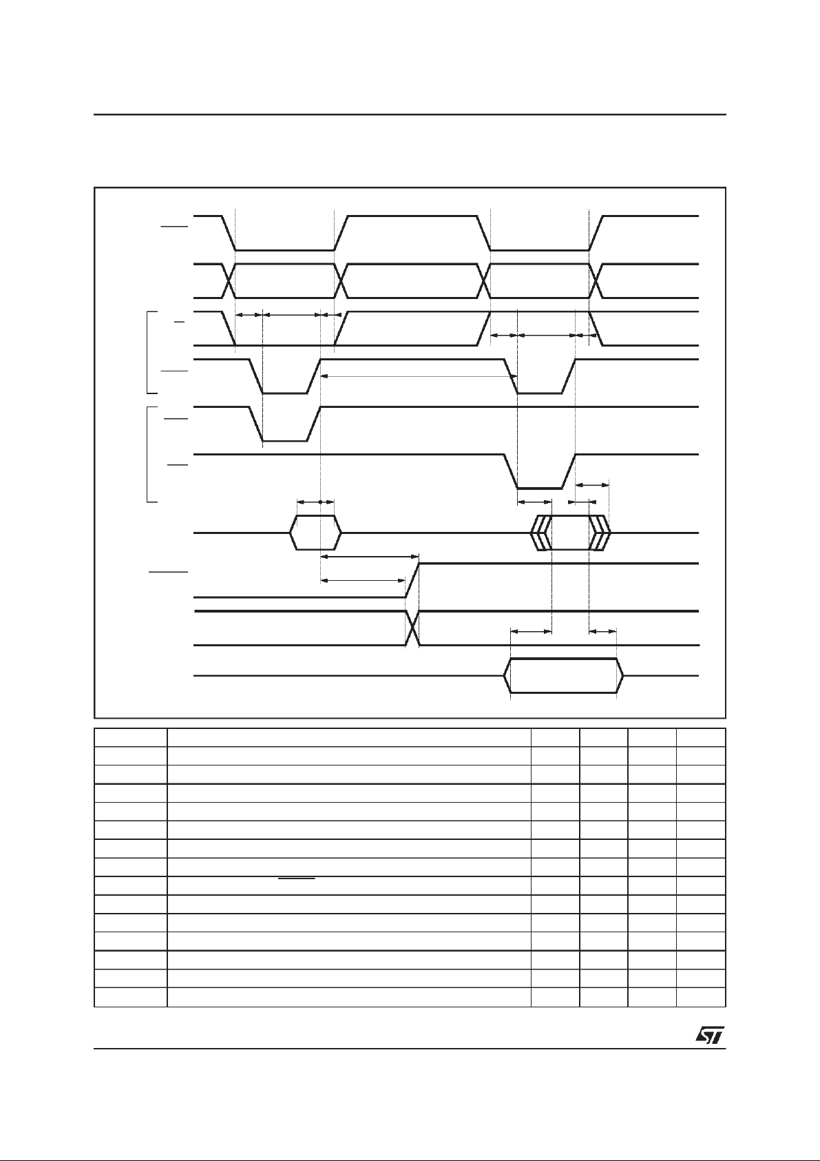
IV.6 - AC ElectricalCharacteristics
WRITE CYCLE READ CYCLE
SCS
SA[0..6]
SR/W
SDS
Motorola mode
WR
RD
Intel mode
SD[0..7]
SINTR
GIO(out),
RELAY
GIO(in)
132
67
8
9
5
142
11
10
13 14
12
OUTIN
75C53004.EPS
Number Description Min. Typ. Max. Unit
1 Address and Control Set-up Time 5 ns
2 Address and Control Hold Time 20 ns
3 Write Enable Low State 45 ns
4 Read Enable Low State 45 ns
5 Access Inhibition High State 70 ns
6 Data Set-up Time 10 ns
7 Data Hold Time 5 ns
8 GIO Output, Relay, SINTR Clear Delay 50 ns
9 GIO Output Hold Time 0 ns
10 Read Data Access Time 35 ns
11 Data Valid to Tristate Time 15 ns
12 Data Hold Time 5 ns
13 GIO Input Delay Time 40 ns
14 GIO Input Hold Time 0 ns
12/84
Page 13

V - FUNCTIONALDESCRIPTION
V.1 - System Architecture
Thechipallowsthe designofa completeFAX,Data
Modem, Hands-Free Telephone and Answering
Machinesystem.A versatile dual port RAM allows
an easy interfacewith most micro-controllers.
V.2 - Modes of Operation
Referto AppendixA for BlockDiagrams.
V.3 - Operations
V.3.1 - Modem TransmitterDescription
The signal pulses are shapedin a dedicated filter
further combined with a compromise transmit
equalizersuited fortransmissionover stronglydistortedlines.3 differentcompromiseequalizersare
availableand can be selectedby software.
V.3.2 - Modem Receiver Description
Thereceiver section handlescomplex signals and
uses a fractionallyspacedcomplex equalizer. It is
able to copewith distant modem timing driftsup to
-4
asspecified in the ITU-Trecommendations.It
10
also compensatesfor frequency drift up to 10Hz
and for phase jitter at multiple and simultaneous
frequencies.
V.3.3 - Tone GeneratorDescription
Fourtonescanbesimultaneouslygeneratedby the
ST75C530/540. These tones are determined by
theirfrequenciesandbytheoutputamplitudelevel.
A set of specific commandsare also available for
DTMFgeneration.Anyof the4 tonegeneratorscan
be output independentlyeither on the Audio DAC
or the line DAC.
V.3.4 - Tone DetectorDescription
During TONE (respectively TONECID) Mode sixteen (respectively eight) tones can be simultaneouslydetected by the ST75C530/540.Each of the
tonesto be detectedis defined by the coefficients
ofa 4th orderprogrammableIIR. Detectionthresholdsare programmablefrom -51dBmupto -6dBm.
These primary detectors can detect tone up to
3.3kHz(sampling rate 7.2kHz in all modes). They
also have a programmable internalwiring feature
(seeChapter IX).
Inallmodes,exceptHandset(HANDSET)andFull
Duplex V.32bis/V.32/V.22bis/V.22 (Modem)
modes, 4 additional tone detectors (each of them
being a 4th order programmable IIR) are concurrently running. In Handset mode only 2 additional
tone detectorsare available. Detection thresholds
areprogrammablefrom-51dBmup to-6dBm.This
secondary programmable detector can detect
tones up to 1.8kHz by default set-up with a sam-
ST75C530- ST75C540
pling rate at 4.8kHz. But this 4 additional tone
detectorscan also detect tonesup to 3.3kHz with
a samplingrate at 9.6kHz. In order to avoid wrong
detectgion,relativedetectgionis also provided.
V.3.5- V.21Channel2 FlagDetectorDescription
InalltheReceiveFAXModes,includingV.21Channel 2 Mode, the ST75C530/540 processes a V.21
Flag“7E” detector,eitherin the idle state,the train
sequenceor the data mode. The detection timeis
3 consecutive flags to detect and 1 byte to loose
the detection.
V.3.6 - HDLC Description
In all FAXModes (MODEM), including V.21 Channel 2 Mode, and also Full Duplex
V.32bis/V.32/V.22bis/V.22 (Modem) modes, a
HDLC framing and deframing is supported by the
ST75C530/540. The number of transmitted flags
canbe programmed.
V.3.7 - UART Description
In Full Duplex V.32bis/V.32/V.22bis/V.22 Modem
ModesandTONECIDV.23receivemode,aparallel
UART is performed by the ST75C530/540. This
UARTmanagethe Break signaleitherat thetransmit and the receive bit stream. The Data format
supportedare7 and 8 bit of Data;even, odd orno
Parity,1 or 2 stop bits.
V.3.8 - DTMF Detector Description
ADTMF Detectoris includedin theST75C530/540,
it allows detection of valid DTMF Digits. A valid
DTMF Digit is defined as a dual tone with a total
powerhigher than -43dBm,a durationhigher than
40msanda differentialamplitudewithin±8dB.This
DTMF Detector is enabled in all modes except in
Fax Modem,Data Modem and Handset modes. It
is also enabledin V.21 Channel 2 ReceiveMode.
The DTMF thresholds and duration can be
changed from they default value by overwriting
DSP’s RAM locations. In the default setup, this
detectoris compliantwith the NET4standard.The
frequencydeviationcan bechangedby overwriting
the default DTMF’s filterscoefficients.
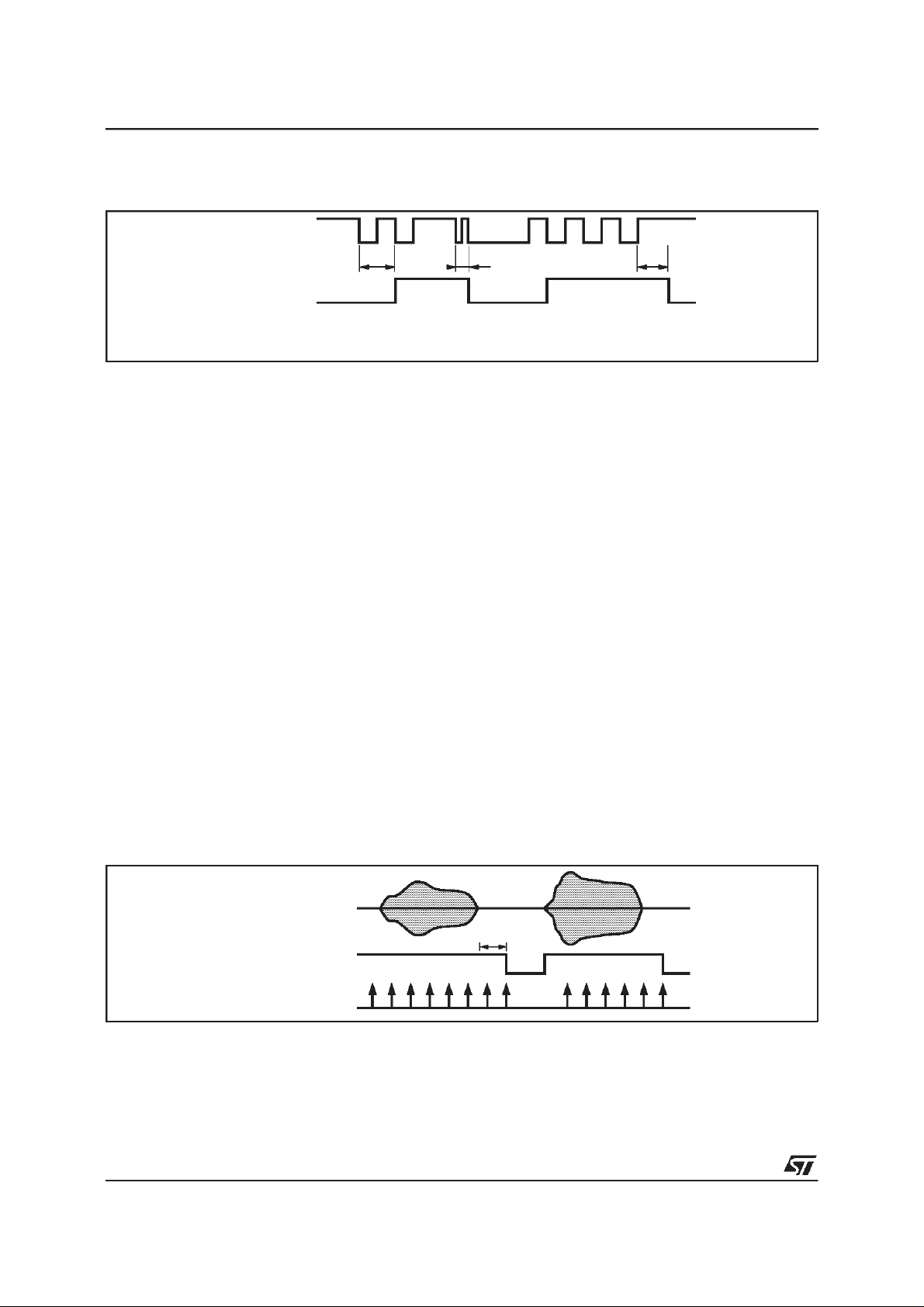
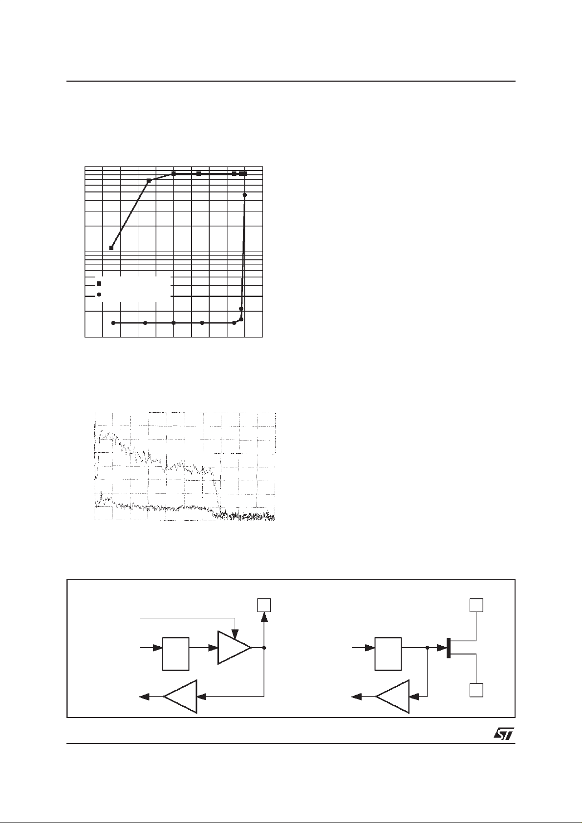
V.3.9 - Ring Detector
This detector detects RING signal from 15Hz to
68Hz, it can be programmed to expand the minimum and maximum detection frequency up to
12Hz(formin)and 144Hz (formax). The detection
time is equal to one period of the ring signal, and
theloosetimeto the minimum between oneperiod
of the ring signal and the inverse of the minimum
frequency.
Theassociated STA_RINGstatus is asFigure 1.
13/84
Page 14
ST75C530- ST75C540
V - FUNCTIONALDESCRIPTION (continued)
Figure1
RING
T1
STA_RING
1/Fmax prog. < T1< 1/Fmin prog.
T2 < 1/Fmaxprog.
T3
1/Fmin prog.
≈
T2 T3
75C53005.EPS
V.3.10 - VOCODER Description
The Vocoder mode allows the implementation of
an answering machine function. In the CODER
mode the received samples from one of the two
analog inputs, Line or Audio, are compressedby
the ST75C530/540and written into the dual port
RAM Vocoder Buffer (VOCxxx). At the same time
the ST75C530/540 is looking for an incoming
DTMFtone and 4 different programmabletones.
In the DECODER mode thecompressedsamples
are read from the dual port RAM, decompressed
and transmitted to one of the two analog output,
Line or Micx. The ST75C530/540 synthesises an
estimation of its echo and subtracts it from the
received signal. At the same time the
ST75C530/540 is looking for an incoming DTMF
tone and 4 differenttones.
Twoalgorithmsof voicecoding are implemented:
- Low bitrate speech coder (4800bps or 5300bps
with forwarderrorcorrection).
- ADPCM (STproprietaryalgorithm)at 32, 24 and
16Kbps.
If the low bit rate coder algorithm is selected the
ST75C530/540has the capability to slow down or
speed up the DECODER flow up to
±50%. This
Figure2
functionallows a quick message listening if speed
up is used,or at the opposite if slowdown is used,
an enhancementof the voice intelligibility.
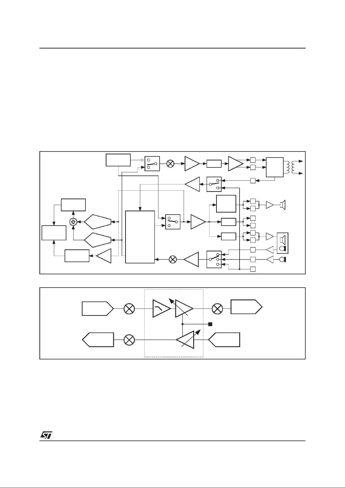
V.3.11- VoiceActivity Detector (VAD)
In CODER Mode, for both of the Voice Coding
algorithms, a Voice Activity Detector is implemented while coding by the ST75C530/540. The
STA_109 bit and STA_109Fbit reflect thestate of
the VAD.After the CONF command the VADis on
(assume voice). The default time-out to detect silenceis2 secondsandtheset-uptimeto detectthe
voiceis 15ms. This VADinformationis alsocopied
into the Receive Buffer Status Word MSB (VOCSTA bit7). This detector is fully programmable in
levelsensitivity(down to -60dBm),hysteresis, and
variouscriteria.
An optional silence suppressor is implemented in
the Coder section to suppress long silence in the
incoming message. When enabled (CONF_SUPSILequal1) if a long silenceis detected(STA_109
equal0) theST75C530/540stopsgeneratingBuffer Interrupts.After that if a voiceis againdetected
theST75C530/540will resume the BufferInterrupt
mechanism.
14/84
Rx Signal
STA_109
(or VOCSTA bit 7)
Interrupt (IT1)
2s
75C53006.EPS
Page 15
V - FUNCTIONALDESCRIPTION (continued)
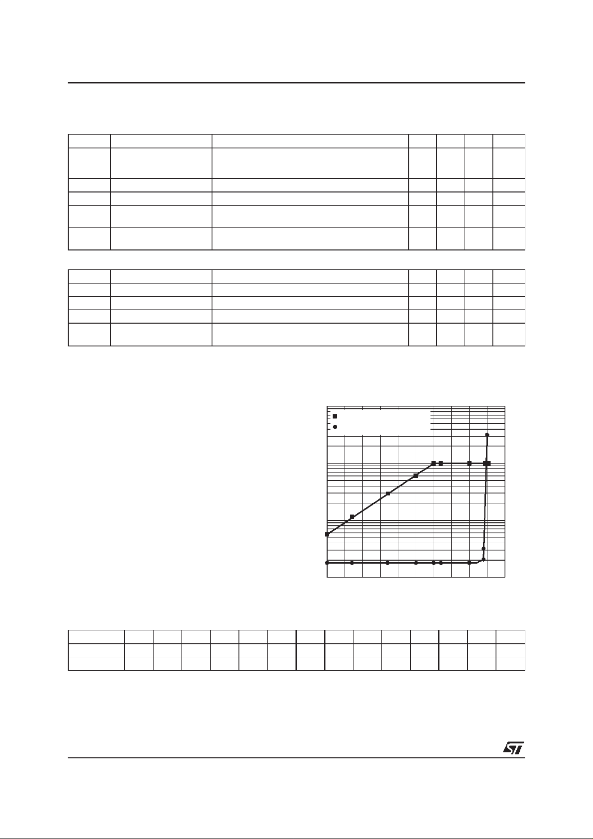
V.3.12 - TelephonyFunctions
ST75C530/540 telephony software provides both
handset and handsfree modes. ST75C530/540is
connected to the phone line through a D.A.A.,
handset and loudspeaker are connected to
ST75C530/540through amplifiers.
Though the D.A.A. hasto comply withmodem/fax
regulationsin most of the applications,the microphone and the earphone amplifier gains will be
adjustedin compliance with the telephony regula-
Figure3 : Handset/HandsfreeMode Operation
ST75C530- ST75C540
tions.Thesoftwareimplementedin ST75C530/540
allows functionssuch as softclipping,AGC in both
modes,andfullduplexmodein handsfree(seeFigure 3).
V.3.12.1 - HandsetMode
In handsetmode, all the attenuations(_SPKGAIN,
_TXGAIN, _MIKGAIN) are f rom 0dB to -inf
(32768steps).AGC andsoftclipping functions can
beenabledanddisabledbysoftware(seeFigure4).
CODER
AGC
DUAL
RAM
INTERFACE
2 TONE
DETECTORS
AGC
Figure4 : HandsetMode
MIC2
SPK2_1
SPK2_2
2 TONE
GENERATOR
DG
HANDSFREE/
HANDSET
ALGORITHMS
_MIKGAIN
_SPKGAIN
ATT_TX
ATT_MIC
AGC= F(I
Softclipping
AGC= F(I
ADC
ADC
LINE
LINE
DAC
)
)
MUTEDAC
MUTE
[0..-30]dB
Step 3dB
_TXGAIN
DP_RING
RxA
MUTE
MUTE
TxA1
TxA2
TxA1
15
14
TxA2
11
RxA
1
2
SPK1
76
SPK3
77
78
79
SPK2
9
MIC2
8
MIC1
10 MIC3
HYBRID
Line
75C53007.EPS
75C53008.EPS
15/84
Page 16
ST75C530- ST75C540
V - FUNCTIONALDESCRIPTION (continued)
Tx Characteristics
Symbol Parameter Test Conditions Min. Typ. Max. Unit
Gtx Transmit Gain _MIKGAIN=7FFF,_TXGAIN=7FFF, AGC disabled
Ntx Transmit noise 2kΩbetween MIC2 and GND -73 dBmp
Mmic Microphone mute V
VLpeak Transmit softclipping
level on TxA1-TxA2
Dtx Transmit distortion _MIKGAIN=7FFF,_TXGAIN=7FFF, AGC disabled
MIC2
_MIKGAIN=7FFF,_TXGAIN=7FFF, AGC disabled
see Figure 3, V
see Figure 3, V
= -21dBV
V
MIC2
= -9dBV
V
MIC2
= -21dBV 60 dB
= -9dBV
MIC2
= -9dBV
MIC2
Rx Characteristics
Symbol Parameter Test Conditions Min. Typ. Max. Unit
Grx Receive Gain _SPKGAIN=7FFF,AGC disabled, V
Nrx Receive noise -79 dBmp
Mrx Mute V
Dtx Receive distortion
(SPK2 output)
= dBV 60 dB
RXA
_SPKGAIN=7FFF,AGC Disabled,V
= -16 dBV 6 dB
RXA
= -16dBV 2 %
RXA
18
8
2.5 Vpp
2%
dB
dB
AGC
The line current information is coming from the
D.A.A.onDP_RINGpin (frequencycoded information using by example a TS555 general purpose
timer).The AGChas a 6dBdepth. Theattenuation
table can be loaded to comply with each country
regulation.Thedefault table has the followingval-
Figure 5 : SoftclippingStatic Gain
Tx Softclipping and Distortion
(mV
10
) D(%)
RMS
4
VTxA1-TxA2(V
RMS
)
Distortion
ues. The value of the AGC gainis applied to both
Txand Rx path(see Table1).
3
The address of the table is given in the register
10
@_TABLE.
The table length is 53. The AGC is enabled using
CONF or MODC command (see paragraph ”VII COMMANDSETDESCRIPTION”.
Oncethe AGCisrunning,it ispossibletofreezethe
10
2
AGC gain with the register AGC_FRZ.
Softclipping
Thesoftclippingintroducesa 12dBgainand has a
18dBdepth.
The sof tclipp ing value is half digital range
(4000 Hex) (see Figure 5).
10
V
MICX
10
(mV
2
)
RMS
10
Table 1 : AGCGain versus PeriodInformation
Period (ms) <9 10 10.8 11.6 14.5 13.3 14.1 15.5 16.6 17.5 18.3 19.1 20 >20
Table Index <13 13 14 15 16 17 18 19 20 21 22 23 24 >24
Gain (dB) 0 0.7 1.5 2.2 3 3.4 4 4.5 4.8 5.1 5.4 5.6 5.8 6
12
10
8
6
4
2
0
3
75C53009.EPS
16/84
Page 17
ST75C530- ST75C540
V - FUNCTIONALDESCRIPTION (continued)
V.3.12.2- HandsfreeMode
The handsfree uses a MIC1 and a SPK1 as microphone and loudspeaker interface (see Figure 6).
Figure6 : HandsfreeMode: Full Duplex
MIC1
SPK1P
SPK1N
_MIKGAIN
_SPKGAIN
+
-
ADAPTIVE
FIR
FILTER
ACOUSTIC
FILTER
NLMS
Softclipping
ATTENUATOR
CONTROL
AGC = F(I
ADAPTIVE
NLMS
)
L
AGC = F(I
ADAPTIVE
ATTENUATOR
L
ADAPTIVE
FILTER
)
_TXGAIN
TxA1
TxA2
FIR
RxA
+
Tx Characteristics
Symbol Parameter Test Conditions Min. Typ. Max. Unit
Gtx Transmit Gain _MIKGAIN=7FFF,_TXGAIN=7FFF ,AGCdisabled,
= -21dBV
V
MIC1
24 dB
Ntx Transmit noise 2kΩbetween MIC1 and GND -70 dBmp
Mmic Microphone mute V
Dtx Transmit distortion _MIKGAIN=7FFF,_TXGAIN=7FFF,AGC disabled,
= - dBV 60 dB
MIC1
= -9dBV
V
MIC1
2%
Rx Characteristics
Symbol Parameter Test Conditions Min. Typ. Max. Unit
Grx Receive Gain _SPKGAIN=7FFF, AGC disabled, V
Mrx Mute 60 dB
Dtx Receive distortion
_SPKGAIN=7FFF, AGC disabled, V
(SPK1 output)
= -33dBV 24 dB
RXA
= -33dBV 2 %
RXA
75C53010.EPS
AGC
TheAGC hasthe samebehaviorasin Handsetmode.Furthermore,the maximumgainadded by AGCcan
be fixed by using the RX_GAINMAXand TX_GAINMAXregisters.
Softclipping
SeeFigure 7.
SystemStability
Parameter Test Conditions Min. Typ. Max. Unit
Loop attenuation in Rx RxA to TxA1-TxA2 Speaker gain is12dB, Mike gain is14dB 20 dB
Loop attenuation in Tx MICx to SPK1P-SPK1N Analogique sidetonenot used
20 dB
(see DAA schematics)
It is possible to add some gain switching in the Tx and Rx path (to reduce the gain of the loop) by using
the GAIN_RCV and GAIN_XMTregisters.
17/84
Page 18
ST75C530- ST75C540
V - FUNCTIONALDESCRIPTION (continued)
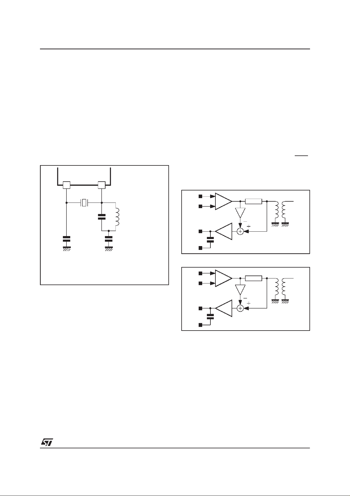
Figure7 : SPK1Distortion versusRxA
Rx Softclippingand Distortion
(mV
10
10
10
Figure8 : Speakerand LineTxPower Spectrums
Fxd Y O
Note : Acoustic echo from speaker to microphone input with no
) D (%)
RMS
3
2
VSPK1 (V
RMS
)
Distortion
2
10
(mV
V
MIC2
POWER SPEC1
POWER SPEC2
0.0
0.0
dBm
RMS
V2
dB
RMS
Vv2
-80.0
-80.0
local speech. Receiving speechon line input.
64Avg
64Avg
Speaker Output
Line Tx
)
RMS
0%Ovlp
0%Ovlp
Hz 5k
Ftop
Ftop
10
12
10
8
6
4
2
0
3
V.3.13 - Low Power Mode
Sleepstatecanbeattainedby aSLEEPcommand.
Whenin sleepmode,thedualportRAMis unavailable and the clocksare disabled.
When entering the low power mode, the
ST75C530/540stopsits oscillator,all theperipheralsof theDSPcore arestoppedin orderto reduce
the power consumption. The dual port RAM is
madeinaccessible.
The ST75C530/540can be awakenedby a hardware reset,a RINGsignal or a dummywrite atany
locationin the dual portRAM.
There is a maximum time of 20ms to restart the
oscillator after waking up and an additional 5ms
after the interrupt to be able to accept any commandcoming from the host.
V.3.14 - Reset
After a hardware reset, or an INIT command, the
ST75C530/540 clears all its internal memories,
clearsthe wholedual port RAM andstarts to initialize the delta sigma analog converters.As soon as
75C53011.EPS
these init ializations are complete d, t he
ST75C530/540 generates an interrupt IT6 (commandacknoledge)andis programmedtosendand
receivetones,thesampleclockare programmedto
9600Hz.Thetotal durationofthe resetsequenceis
about 5ms. After that time the ST75C530/540 is
readytoexecutecommandssentbythehostmicrocontroller.Thedurationoftheresetsignalshouldbe
greaterthan700ns.
V.4- Modem Interface
V.4.1 - AnalogInterface
Referto BlockDiagram on page 7.
V.4.2 - General I/O and Relay Interface
16 pins are dedicatedto the generalI/O port. Two
75C53012.EPS
arededicatedto Relaydriver.Theequivalentschematic is as follows: seeFigure 9.
Figure9
IODIR0[x]
IODATA0[x]
IODATA0[x]
18/84
(write)
(read)
GIO0[x]
QD
IORELAY[y]
(write)
QD
RELAY[y]
N
IORELAY[y]
(read)
RGND
75C53013.EPS
Page 19
V - FUNCTIONALDESCRIPTION (continued)
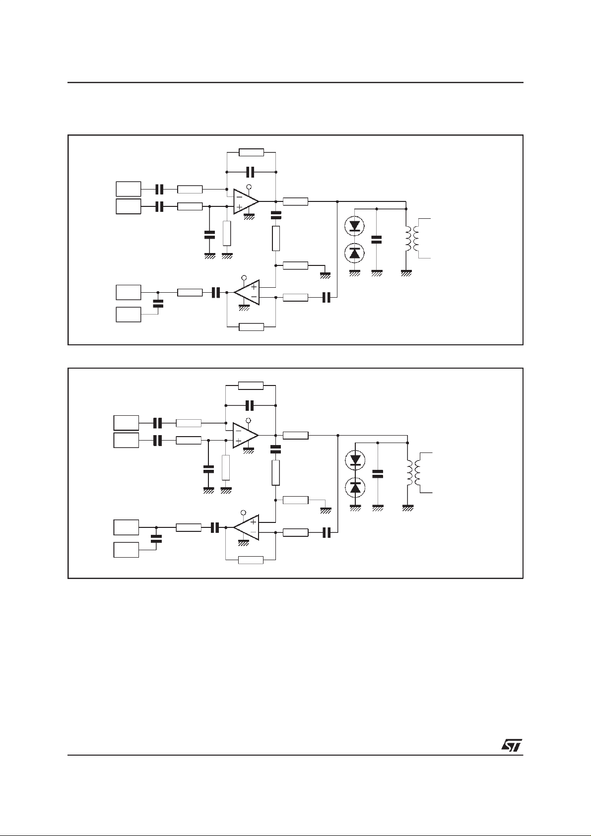
V.4.3 - Crystal
The crystal frequency must be 44.2368MHz for
ST75C530and 49.152MHzfor ST75C540withan
accuracybetterthat±100 ppm. When using a third
harmoniccrystal the schematicmust beas follow:
seeFigure 10.
Thecrystal featuresare :
- third harmonic,
- parallel, loadcapacitance= 10pF,
- æ 100ppm from 0
<50Ω,
-R
S
o
Cto70oC,
- ATcut(example : SM55-10 MATEL).
Figure10
ST75C540
EXTALL XTALL
*
**
XTAL H3: 44.2368MHz (ST75C530)
73 72
XTAL H3 **
C2
27pF
COG
C1
10pF
COG
Wire wound inductor recommanded (Example : SIGMA-SC30)
Thrird harmonic (Example : MATEL-SM55-10)
49.152MHz(ST75C540)
L*
H (ST75C530)
0.82
µ
0.68µH(ST75C540)
Cb
10nF
V.4.4 - TypicalApplicationSchematic
TheFigure 11is a blockdiagramdesignedtoallow
transmission of fax signals up to +0dBmand sine
waveup to +6dBmon the telephoneline. It allows
receptionoffaxsignalsupto0dBmandsinewaves
upto +6dBm.Figure12isablockdiagramdesigned
ST75C530- ST75C540
to allow transmission of Modem signal up to 10dBmand receptionup to -10dBm.TheOPAmps
are +12/0V powered. With this application schematictheoutofbandtransmitspectrum(from4kHz
to 50kHz) is below-72dBm.
Figures13and14areexamplesofapplicationschematicswhichrespectsgainvalue(respectivelyforfax
and voice application and for Modem application)
andtheminimumdifferentialloadonTxA1andTxA2.
V.4.5 - Host Interface
Thehost interface is seen by the microas a 128x8
RAM, withadditional registers accessiblethrough
an8-bit address space. Aselection Pin (INT/MOT)
allowsto configurethe hostbus foreither INTELor
MOTOROLAtype control signals.
Figure 11
Figure 12
75C53014.EPS
TxA1
TxA2
RxA
V
CM
TxA1
TxA2
RxA
V
CM
2.2nF
2.2nF
+8dB
-10dB
0dB
0dB
600
Ω
-1/2
600Ω 1:1
-1/2
1:1
Line
75C53015.EPS
Line
75C53016.EPS
19/84
Page 20
ST75C530- ST75C540
V - FUNCTIONALDESCRIPTION (continued)
Figure13 : FaxMode
56.2kΩ 1%
270pF
18.2kΩ 1%
TxA1
TxA2
470nF
470nF
18.2kΩ1%
470pF
+12V
GND
47.5kΩ
560Ω
470nF
30kΩ 1%
1:1 *
22nF
RxA
VCM
Figure14 : DataMode
470nF
TxA1
TxA2
470nF
RxA
VCM
1.2kΩ
2.2nF
18.2kΩ 1%
18.2kΩ 1%
470pF
1.2kΩ
2.2nF
+6V+6V
+6V+6V
+12V
GND
10kΩ 1%
24kΩ 1%
270pF
GND
47.5kΩ
+12V
GND
+12V
6.21kΩ 1%
+6V
24.3kΩ 1% 470nF
560Ω
470nF
30kΩ 1%
6.21kΩ 1%
+6V
24.3kΩ 1%
470nF
+6V +6V
* Insertion loss = 2.5dB between 0 and 3.4kHz
+6V +6V
+6V470nF
1:1 *
22nF
+6V470nF
75C53017.EPS
20/84
33kΩ 1%
* Insertion loss = 2.5dB between 0and 3.4kHz
75C53018.EPS
Page 21

VI- USER INTERFACE
VI.1- Dual Port Ram Description
The dual port RAM is the standard interface between the hostcontroller and the ST75C530/540,
for either commandsor data. This memory is addressedthrougha7-bitaddressbus. The locations
from$00 to $3Fare RAM location,while locations
from $40 to $60 are control registers dedicatedto
the interrupt handling and the generalIO port and
Relayoutput.
Severalfunctionalareasaredefinedin thedualport
RAMmapping :
- the commandarea,
- the report area,
- the status area,
- the optionalstatus area,
- the data bufferarea,
- the interruptcontrol area,
- the generalI/Oand Relay Outputarea.
VI.1.1 - Mapping
VI.1.1.1- CommandArea
The command area is located from $00 to $04.
Address $00 holds the command byte COMSYS,
and the next four locations hold the parameters
COMPAR[0..3].Thecommandparametersmustbe
enteredbeforethecommandwordis issued.Once
thecommandhasbeenentered,thecommandbyte
isresetandanacknowledgereportisissued.Anew
command shouldnot be issuedbeforetheacknowledgecounterCOMACK is incremented.
VI.1.1.2- Report Area
The report area is located from address $05 to
address$07. Location$05holdstheacknowledge
counter COMACK. Each time a command is acknowledged, the report bytes COMREP[0..1] (if
any) are written by the ST75C530/540 into locations$06 and$07, and the content ofCOMACKis
incremented. This counter allows the
ST75C530/540 to accurately monitor the commandprocessing.
VI.1.1.3- Status Area
Thestatusareaislocatedfromaddress$08to$0B.
TheerrorstatuswordSYSERRislocatedat address
$08.Thiserrorstatuswordisupdatedeachtime an
errorconditionoccurs. An optionalinterruptionIT0
mayadditionallybetriggeredinthe caseofanerror
condition. Locations$09 and $0A hold the general
statusbytesSTATUS[0..1].Themeaning ofthebits
dependsonthemodeof operation,andisdescribed
inChapter VIII.The thirdbyteat address$0B holds
theQualityMonitorbyte STAQUA.
ST75C530- ST75C540
VI.1.1.4- OptionalStatus Area
The user can program (through the DOSR command) the four locations STAOPT[0..3]of the Optional Status Area ($0C to $0F) for the real time
monitoring of fourarbitrary memory locations.
VI.1.1.5- Data Buffer Area
The data area is made of four 8-byte buffers
(see ParagraphVI.1.3“Host InterfaceSummary”).
Two are dedicated to transmission and the two
others to reception. Each of the four buffers is
attachedto astatusbyte.the meaningof thestatus
byte depends on the selected format of transmission. Within eachbuffer,D0 representsthe firstbit
in time.
VI.1.1.6- VOCODERBuffer Area
(VOCODERMode)
Thisareais made ofa 18+2byte buffer.Thisbuffer
contains the VOCODER frame. The first 18 bytes
VOCDATAcontain the coded frame and the other
2 bytes VOCCORR the Error corrections bit (only
valid in low bit ratemode).
In theReceiveMode (CODER)the ST75C530/540
codesthe received samplesand writes the correspondingbytes in thebuffer.If thelow bitratemode
is selected,the ST75C530/540computesthe Error
corrections2 bytesand writesthem in the buffer.
In the Transmit Mode (DECODER) the
ST75C530/540reads the 18codedbytes decodes
themand sendsthe signaltothe analogoutput.In
the low bit rate mode if the Error Correction is
enabled, prior the decoding, the ST75C530/540
reads the 2 Error Correction Bytes and, if any,
correctsthe first 18 bytes.
A mechanism of flags to share the buffer access
betweentheST75C530/540and thehostcontroller
is controlledby the VOCSTAbyte :
- In CODER mode, when the ST75C530/540 has
finis-hed writing the VOCDATA and VOCCORR
bytes, it writes$14 in VOCSTAand generate an
InterruptIT1. The host must read the Data buffer
then clear the VOCSTAbyte.
- In DECODER mode, the host must feed the
VOCDATAand, optionaly,the VOCCORRbytes,
then write $14 (if lowbit rate) or$12 (if ADPCM)
in VOCSTA. The ST75C530/540 will read the
VOCDATA and VOCCORR bytes, clear the
VOCSTA and generate an Interrupt IT1. A silence frame can be generated, in either low bit
rate or ADPCM mode, by writing 00 in all the
VOCDATAbuffer, including the Error Correction
Bytes VOCCORR.
21/84
Page 22

ST75C530- ST75C540
VI - USER INTERFACE (continued)
VI.1.1.7- InterruptControlArea
Theinterrupt area, that start afterthe address$40
controls the behaviour of the Interrupts mechanism. Register ITSRCR definesthe source of the
interrupt,the registerITMASK allowsindependent
enabling or disabling of any of the interrupt’s
source, registers ITREST0 to ITREST6 reset the
correspondinginterrupt source.
Theseregistersarenotaffectedby aINITcommand,
theyareonlyresetedbya Hardware RESETsignal.
VI.1.1.8- GeneralIO and RelayOutput Area
A set of 5 registers is directly accessible by the
controller to program the General IO pins and
Relay Outputs (see Paragraph VI.1.3 “Host Interface Summary”). Two registers IODIR0 and IODIR1 define the type of the IO pin, either Input or
Output (0 = input, 1 = output), and two registers
IODATA0and IODATA1 define the IO pin signals.
The fifth registerdefines the Relay output signals.
Theseregistersarenotaffectedby aINITcommand,
theyareonlyresetedbya Hardware RESETsignal.
The general IO are setup as input after the power
up or an hardware RESET. The relay output are
openafter powerup or an hardware RESET.
VI.1.2- Interruptions
The ST75C530/540 can generate 7 interruptsfor
the controller. The interrupt handling is made with
a setof registerslocatedfrom $40 to $5F.
The interruptions generated by the ST75C530/540
come from several sources. Once the
ST75C530/540raisesan interrupt,a signal(SINTR)
is sent to the controller. The controller has thento
processtheinterruptandclearit.Theinterruptsource
can be examined in the interrupt source register
ITSRCR located a $50. According to the ITSRCR
bits, the interrupt source can be determined. Then
writing a zero at one of the memorylocation$40 to
$46 (Reset InterruptRegister ITRES[0..6]) will reset the correspondinginterrupt (and thus acknowledgeit).The sourceoftheinterruptcanbe masked
globally or individually using the Interrupt Mast
register ITMASK located at $4F.
Theinterrupt sources are :
- IT0 : Error
This signifiesthat an error has occurred and the
error code is available in the error status byte
SYSERR.Thisbytecanbe selectivelyclearedby
the CSE command.
- IT1 : VOCODERBuffer
Each time the ST75C530/540 have coded a
frame (CODER Mode) or decodeda frame (DECODERMode) this interrupt is generated.
- IT2 : TxBuffer
Each timethe ST75530/C540freesa databuffer,
this interruptis generated.
- IT3 : Rx Buffer
Each time the ST75C530/540 has filled a data
buffer,this interrupt is generated.
- IT4 : StatusByte
This signifies that the status byte has changed
and must be checkedby thecontroller.
- IT5 : Low Power Mode
TheST75C530/540hasbeenawakenedfromthe
low power mode by a low level on theRING pin
or a dummywrite issued bythe host.
- IT6 : CommandAcknowledge
This signifies that the ST75C530/540 has read
the last command entered by the host, incremented the command counter COMACK, and is
readyfora new command.
Note: Interrupt registers are clearedaftera Hardware RESET. These registers are not affectedby
a INIT Command.
22/84
Page 23
VI- USER INTERFACE(continued)
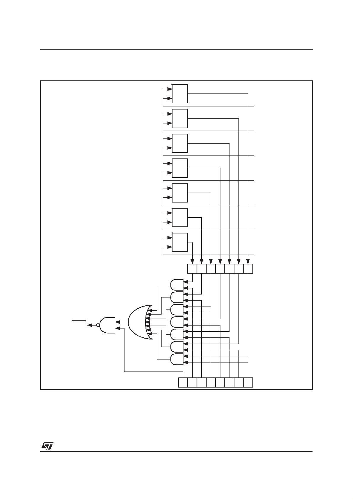
Figure15 : FunctionalSchematic
ST75C530- ST75C540
ITREST 0
(write only)
ITREST 1
(write only)
ITREST 2
(write only)
ITREST 3
(write only)
ITREST 4
(write only)
ITREST 5
(write only)
ITREST 6
(write only)
R
Q
S
IT0 : Error
R
Q
S
IT1 : VOCODER
R
Q
S
Buffer
IT2 : Tx Buffer
R
Q
S
IT3 : Rx Buffer
R
Q
S
IT4 : Status
R
Q
S
IT5 : Low Power
R
Q
S
IT6 : Command
SINTR
(open drain)
ITSRCR
(read only)
ITMASK
(read write)
0123456
01234567
75C53019.EPS
23/84
Page 24
ST75C530- ST75C540
VI - USER INTERFACE (continued)
VI.1.3- Host Interface Summary
Address (hex) Description Size (Byte) Mnemonic
COMMAND AREA
$00 Command 1 COMSYS
$01-$04 Command Parameters 4 COMPAR[0..3]
REPORT AREA
$05 Acknowledge Counter 1 COMACK
$06-$07 Report 2 COMREP[0..1]
STATUS AREA
$08 Error Status 1 SYSERR
$09-$0A General Status 2 STATUS[0..1]
$0B Quality Monitor 1 STAQUA
$0C-$0F Optional Report 3 STAOPT[0..3]
DATA BUFFER AREA (FAX Modes andData Modes)
$1C Data Rx Buffer 0 Status 1 DTRBS0
$1D-$24 Data Rx Buffer 0 8 DTRBF0[0..7]
$25 Data Rx Buffer 1 Status 1 DTRBS1
$26-$2D Data Rx Buffer 1 8 DTRBF1[0..7]
$2E Data Tx Buffer 0 Status 1 DTTBS0
$2F-$36 Data Tx Buffer 0 8 DTTBF0[0..7]
$37 Data Tx Buffer 1 Status 1 DTTBS1
$38-$3F Data Tx Buffer 1 8 DTTBF1[0..7]
VOCODER BUFFER AREA (VocoderMode)
$1C Vocoder Buffer Status 1 VOCSTA
$1D-$2E Vocoder Buffer Data 18 VOCDATA
$2F-$30 Vocoder Buffer Corrector 2 VOCCORR
INTERRUPT AREA
$40-$46 Reset Interrupt Register 7 ITREST[0..6]
$4F Interrupt Mask Register 1 ITMASK
$50 Interrupt Source Register 1 ITSRCR
GENERAL IO AND RELAY
$60 I/O Direction 0 1 IODIR0
$61 I/O Direction 1 1 IODIR1
$62 I/O Data 0 1 IODATA0
$63 I/O Data 1 1 IODATA1
$64 I/O Relay Register 1 IORELAY
Note : Registers which address is higheror equal to $40 are not affectedby a INIT Command or a Low Power wake-up. They are reseted
only by a HardwareRESET.
24/84
Page 25

VI - USER INTERFACE (continued)
VI.2 - CommandSet
The Command Set has the following attractive
features:
- user friendlywith easyto remembermnemonics,
- possibility of straightforwardexpansionwith new
commands to suit specific customer requirements,
- easy upgrade of existingsoftwareusingprevious
modembased SGS-THOMSONproducts.
Thecommandsethasbeendesignedtoprovidethe
necessaryfunctionalcontrolon theST75C530/540.
Eachcommand is classifiedaccordingto its syntax
and the presence/absence of parameters. In the
case of a parametriccommand, parameters must
first be written into the dual port RAM before the
command isissued.Acknowledgeand errorreport
isissuedfor each commandentered.
VI.2.1- CommandSet Summary
VI.2.1.1- OperationalControl Commands
INIT Initialize. Initialize the modem engine.
Setall parameterstotheirdefaultvalues
and wait for commands of the control
processor.Non parametric command.
IDT Identify.Returnthe productidentification
code. Non parametriccommand.
SLEEP Turn to low power mode, the
ST75C530/540 enters the low power
mode and stops its crystal oscillator to
reducepowerconsumption.Inthismode
all the clocks are stopped and the dual
RAM is unreachable.
HSHK Handshake. Begins the handshake
sequence.Themodemenginegenerates
all the sequences defined in the ITU-T
recommendations. A status report
indicatesto thecontrolprocessorthestate
of the handshake. This command only
applies to modes where a handshake
sequence is defined.A CONFcommand
musthavebeen issuedpriorto theuseof
HSHK. Nonparametriccommand.
STOP FAX Sto p. Stop FAX Half-duplex
transmitter.Non parametric command.
RTRA Retrain. Begin a retrain sequence in
V.32bis/V.32 or V.22bis modes as
described in the ITU-T
recommendations(ST75C540only).
ST75C530- ST75C540
SYNC FAXSynchronize.Start/StopofFAXHalf-
duplexreceiver. Parametriccommand.
CSE Clea rStatu sEr r o r.Selectivelyclear stheError
statusbyteSYSERR.Par a m etri ccomman d.
SETGN Set Gain.This command sets theglobal
gainfactor,whichis usedforthetransmit
samples.Parametriccommand.
VI.2.1.2- Data CommunicationCommands
XMIT Transmit Data. Start/stop the
transmission of data. After a XMIT
command,theST75C530/540sendsthe
data contained in its dual port RAM.
FORM Selects the Transmission Format. This
command configures the data interface
for both re ceiver and transmitte r
according to the selected data format.
Parametric command (HDLC, UART or
synchronous).
VI.2.1.3- MemoryHandlingCommands
MWI
MWLO
MW
MRI
MRLO
MR
CR Complex Read. This command allows
MemoryWrite Indirect
MemoryWrite Low Word
MemoryWrite.This commandis usedto
write an arbitrary 16-bit value into the
writable memory lo cation currently
specified by a parameter. Parametric
command.
MemoryRead Indirect
MemoryRead Low Word
MemoryRead.Thiscommandallowsthe
controller to read any of the ERAM or
CROM (ST75C530/540 memory
spaces)locationwithout interrupting the
processor. Parametric command.
the controller to read at the same time
the realand imaginary partof acomplex
valuestoredinadoubleERAMor
CROM location. This feature is very
interesting for eye pattern software
control and for equalization monitoring.
This commandinsures that the real and
imaginary parts are sampled in the
memory at the same time (integrity).
Parametric command.
25/84
Page 26

ST75C530- ST75C540
VI - USER INTERFACE (continued)
VI.2.1.4- Configuration Control Commands
ASEL Select the Analo g path option, like
Microphone input, Speaker attenuation.
Parametriccommand.
CONF Configure. This commandconfiguresthe
modemengine fordatatransmissionand
handshakeprocedures (if any) in any of
the supported modes. The transmission
parametersare set totheirdefaultvalues
and can be modified with the MODC
command.Parametric command.
MODC Modify Configuration. This command
allows mod ification of some of th e
parameters which have been set up by
theCONF command.It canalso be used
to alter the mode of operations (short
train).Parametriccommand.
DOSR Define Optional Status Report. This
command allows the modification of the
optionalstatusreportlocatedinthestatus
areaof the dualport RAM. One can thus
select a particular parameter to be
monitoredduring all modes of operation.
Parametriccommand.
DSIT Define Status Interrupt. This command
allows the programming of the status
word bit that will generate an Interrupt to
thecontroller.Parametric command.
VI.2.1.5- Tone Generation Commands
TONE SelectTone .Progr amsthetonegenerator ( s)
for the desired default tone(s ) . Additi onal
mnemonics provide quick progra m m i ng of
DTMF tonesor other currently used tones.
Parametriccommand.
DEFT Define Tone. Programs the tone
generator(s)for arbitrary tone synthesis.
Parametriccommand.
TGEN Tone Generator Control. Enabl es or
disables the tone generator(s).
Parametriccommand.
VI.2.1.6- Tone Detection Commands
TDRC Read Tone Detector Coefficient. Read
one Tone Detect or Coefficient.
Parametriccommand.
TDWC Write Tone Detector Coefficient. Write
one Tone Detect or Coefficient.
Parametriccommand.
TDRW Read Tone Detector Wiring. Read one
Tone Detector Wiring connection.
Parametriccommand.
TDWW Write Tone Detector Wiring. Write one
Tone Detector Wiring connection.
Parametriccommand.
TDZ Clear Tone Detector Cell. Clear internal
variable s of a Ton e Det ect or Ce ll.
Parametriccommand.
VI.2.1.7- MiscellaneousCommands
CALL Call a Subroutine. Call a subroutinewith
one Parameter.Parametriccommand.
JSR Call a Low Level Subroutine. Call an
internal subroutine with one parameter.
Parametriccommand.
VI.3- CommandSet Short Form
CCI Command
Mnemonic Value Description
XMIT 0x01 Transmit Data
SETGN 0x02 Set Transmit Gain
SLEEP 0x03 Power DowntheST75C530/540
HSHK 0x04 FAX Start Transmitter
RTRA* 0x05 Retrain(V.32bis/V.32andV.22bis)
INIT 0x06 Initialize (Software Reset)
CSE 0x08 Clear Error StatusWord
FORM 0x09 Define Data Format
DOSR 0x0A Define Optional StatusReport
ASEL 0x0B Select the Analog Path Options
TONE 0x0C Generate Predefined Tones
TGEN 0x0D Enable Tone Generator
DEFT 0x0E Define Arbitrary Tone
MR 0x10 Memory Read
CR 0x11 Complex Read
MW 0x12 Memory Write
DSIT 0x13 Define Status Interrupt
IDT 0x14 ReturnProductIdentificationCode
JSR 0x18 Call a Low Level Routine
CALL 0x19 Call a Routine
TDRC 0x1A Tone Detector Read Coefficient
TDRW 0x1B Tone DetectorRead Wiring
TDWC 0x1C Tone Detector Write Coefficient
TDWW 0x1D Tone DetectorWrite Wiring
TDZ 0x1E Tone DetectorClear Cell
CONF 0x20 Configure
MODC 0x21 Modify Default Configuration
STOP 0x25 FAX Stop Transmitter
SYNC 0x26 FAX Synchronize Receiver
MRI 0x28 Memory Read Indirect
MRLO 0x29 Memory Read Low Word
MWI 0x2A Memory Write Indirect
MWLO 0x2B Memory WriteLow Word
* ST75C540 only.
26/84
Page 27

VI - USER INTERFACE (continued)
VI.4 - Status - Reports
VI.4.1- Status
TheST75C530/540has a dedicatedstatusreporting area located in its dual port RAM. This allowa
continuousmonitoring of the status variableswithout interrupting the ST75C530/540.
The first statusbyte givesthe error status. Issuing
of an error status can also be flagged by a maskable interruptfor the controller.The significationof
the error codesare given in Chapter VIII.
Thesecond and thirdstatusbytesgivethegeneral
status of the modem. These status include for
example the ITU-T circuit status and other items
described in Chapter VIII “STATUS DESCRIPTION”. These two status can generate, when a
changeoccurs,an interruptto the controller; each
bit of the two byte word can be masked independently.
The forth byte gives in real time a measure of the
receptionquality.Thisinformationmaybeusedbythe
controllertomonitorthequalityofthereceivedbits.
Four other locations are dedicated for custom
status reporting. The controller can program the
ST75C530/540for a realtime monitoringof any of
its internalRAM location. High byte or low byte of
anyword can thusbe monitored.
VI.4.2- Reports
TheST75C530/540featuresan acknowledgeand
report facility. The acknowledge of a command is
monitored by a counter COMACK located in the
dualportRAM. Eachtime a commandisreadfrom
the commandarea, the ST75C530/540will incrementthiscounter.For instance, whena MR(Memory Read) command is issued, the data is first
writtenin the report area,and thecounteris incrementedafterwards.Thiswayofprocessinginsures
dataintegrity andgives additionalsynchronization
betweenthe controllerand the data pump.
VI.5 - Data Exchanges
The ST75C530/540 accepts many kinds of data
exchange:thedefaultmode usesthesynchronous
parallel exchange. Other modes include HDLC
framingsupport andUART.Detaileddescription of
the Data Buffer Exchanges modes is available in
the paragraph X.
VI.5.1- SynchronousParallel Mode
The data exchanges are made through the dual
portRAM andarebyte synchronousoriented.The
double buffer facilitiesof the ST75C530/540allow
an efficient bufferingof thedata.
ST75C530- ST75C540
VI.5.1.1- Transmit
The controller must first fill at least the first buffer
ofdata (Tx Buffer 0) withthe bits to be transmitted.
In order to perform this operation, the controller
must first check the Tx Buffer 0 status word
DTTBS0. If this buffer is empty, the controllerfills
the data buffer locations(up to 64 bits), and then
writesin DTTBS0the numberof bytescontainedin
the buffer.The controller can then either proceed
with the second buffer or initiate the transmission
witha XMITcommand.
TheST75C530/540copiesthe contentsof thedata
buffer and then clears the buffer status word in
orderto makeit againavailable,then generatesan
IT2interrupt. Thenumber of bytesspecifiedby the
status word is then queued for transmission. The
processgoes on withthetwobuffersuntil an XMIT
commandstops the transmission. After the finishingXMIT command has beenissued, thelastbuffers are emptiedby the ST75C530/540.
Errorsoccurwhenboth buffersare emptywhilethe
transmitbit queueis also empty. Error is signalled
withan IT0interruption to the controller.
VI.5.1.2- Receive
Thecontroller shouldtake careof releasingthe Rx
buffers before the Data Carrier Detect goes true.
Thisismadeby writingzeroin the Rx BufferStatus
0 and 1. The ST75C530/540 then fills the first
buffer,andonce filled sets the statusword withthe
number of bytes received and then generatesan
IT3 interrupt. It then takes control of the second
buffer and operatesthe same way.The controller
must check the status of the buffers and empty
them. Once the data read, the controller must
releasethe used bufferand wait forthe nextbuffer
to be filled.
Error occurs when both buffers are declared full,
and incomingbits continue to arrive from the line.
Erroris signaledby an IT0 interrupt.
VI.5.2 - HDLCParallel Mode
Thismodeimplementspart ofthe High Level Data
Link Control formats and procedures. It is well
suited for error correcting protocols like ECM or
FAXT4/T30recommendations.Itsupportstheflagginggeneration,16-bitFrameCheckSequence,as
well as the Zeroinsertion/deletionmechanism.
VI.5.3 - UARTParallel Mode
This mode implementa 7 or 8 bitdata format,it is
well suited forCaller ID or Minitel applications.
27/84
Page 28

ST75C530- ST75C540
VII - COMMAND SET DESCRIPTION
Commandsare presentedaccording to the followingform :
COMMAND Command Name Meaning COMMAND
Opcode Hexadecimaldigit
XXXXXXXX
Synopsis Shortdescription of the functionsperformedby the command.
Parameters
Field Byte Pos. Value Definition
Name X b..a
Explanation of the parameter
xx *
Default value
Field Name of the addressedbit field.
Byte Index (or addressin the dualport RAM)of the parameterbyte (from1 to4).
Pos. Bit field position inside the parameter byte. Can either be a single position (from 0 to 7, 0
being LSB) or a range.
Value Possibl evaluesforthebit(res p.bitfield).Rangemeansallvaluesareallow ed.Astarmeansa default
value.V al uesareexpressedei therundertheformofabitstrin g,orunderhexadeci malformat.
ASEL ASEL
Opcode: 0B
00001011
Synopsis Select the analog path options. This command select the Attenuation/Muteof the outputs
TxA1/TxA2 and SPK1/SPK2/SPK3.This command selectalso the sourceof the Mic signal
MIC1/MIC2/MIC2and the source of theLine Signal RxA/MIC3.
Parameters
Field Byte Pos. Value Definition
ASEL_ASPK1 1 7..4 0000*
0001
0010
1010
1011
Other
ASEL_MICSEL 2 1..0 00*
ASEL_LINESEL 2 2 0*1Select RxA as line input
ASEL_ESPK1 2 3 0*1SPK1output muted
ASEL_ESPK2 2 4 0*1SPK2output muted
ASEL_ESPK3 2 5 0*1SPK3output muted
ASEL_MTXA 2 7 0*1TxA output normal
Infinity attenuation
30dB attenuation
27dB attenuation
...
...
3dB attenuation
0dB attenuation
Reserved
Select Rx input as MIC1
01
Select Rx input as MIC1
10
Select Rx input as MIC2
11
Select Rx input as MIC3
Select Mic3 as line input
SPK1output normal
SPK2output normal
SPK3output normal
TxA output muted
CALL Call aSubroutine CALL
Opcode: 19
00011001
Synopsis CALLallows to executea part of theST75C530/540firmware with aspecificargument.
Parameters
This instruction can be used with SGS-THOMSON Microelectronics Application Laboratory Support for
specialapplicationsdevelopmentor debuggingneeds.Contact your local representative.
28/84
Field Byte Pos. Value Definition
C_ADDR_L 1 7..0 Low byte of the call address
C_ADDR_H 2 7..0 High byte of the call address
C_DATA_L 3 7..0 Low byte of the argument
C_DATA_H 4 7..0 High byte of the argument
Page 29

ST75C530- ST75C540
VII - COMMAND SET DESCRIPTION(continued)
CONF Configure for Operations CONF
Opcode: 20
00100000
Synopsis CONFallows thecompletedefinitionof theST75C530/540operation, includingthe modeof
operation(Tone, FAXTransmit,Voice Transmit,Voice Receive, DTMFReceiver,...) and the
Modem or VocoderParameters (Standard, speed, ...). Accordingwith the 4 first bits of the
CONFParameterthe ST75C530/540is putinto the following mode of operation.
(4)
Detectors
Yes
No
Yes
No
Yes
No
No
No
Yes
Yes
No
No
No
No
No
No
Yes
Yes
No
No
No
No
No
Yes
Yes
Yes
Yes
Yes
No
No
No
No
(5)
(4)
Answ
Yes
No
No
Yes
No
No
No
No
(6)
CONF_
OPER
0000*
0001
0010
0100
1000
1001
1100
HANDSET/HANDSFREE
1111
Other
Notes : 1.This mode includes V.23/Bell202 FSK Demodulatorand UART.
2.This primary ToneDetectors allows Detectionof signalup to 3.3kHz. (SamplingRate 7.2kHz).
3. Thissecondar yToneDetecto rsallowsDetectionofsignalupto1.8kHz(withSamplingRate4.8k Hz)orupto3.3 kHz(withSamplingRate9.6kHz) .
4.The DTMF detector and Call Progress Tone detector (CPT) are available only forV.21 Channel 2.
5.STA_CPT0,STA_CPT1 and STA_CPT10in STATUS0.
6.STA_CCITT and STA_AT in STATUS1.
7.Not available in V.32bis/V.32.
Mode
TONE
TONECID(1)
DECODER
TRANSPARENT
CODER
ROOM-MONITOR
MODEM
Reserved
Tone
16
6
0
6
0
0
0
0
(2)
Tone
4
(3)
4
4
4
4
4
4
2
(7)
DTMF Ring VAD V.21 Flag CPT
Yes
Yes
Yes
Yes
Yes
Yes
No
Yes
29/84
Page 30

ST75C530- ST75C540
VII - COMMAND SET DESCRIPTION(continued)
Parameters Whenthe CONF_OPERis setto F,selectingtheModem Mode ofoperation,theparameters
have the followingmeaning :
Field Byte Pos. Value Definition
CONF_OPER 1 3..0 1111 Select Modem Mode
CONF_ANAL 1 4 01Normal mode
CONF_PSTN 1 5 01PSTN (carrierdetect set to -43/-48dBm)
CONF_AO 1 6 01Answer mode
CONF_DTINIT
170
(only in tone mode)
CONF_MODE 2 5..0 0
Other
CONF_TXEQ 2 7..6 0
CONF_CAR 3 0 011800Hz carrier(V.17/V.33 only)
CONF_TCM 3 1 01Treillis coding not allowed (V.32 only)
CONF_SP0 3 7..4 xxx1
xx1x
x1xx
1xxx
CONF_SP1 4 2..0 xx1
Notes : 8. Withconf 8000 00 00 the coefficients of secondary tone detectorsare notinitialized.
9. ST75C540 only.
10. V.22bis, V.22,V.32bis and V.32 modes ST75C540 only.
Analog loop back (testmode only)
Leased line (carrier detect -33/-38dBm)
Originate mode
Global init of secondary tone detector
1
Partial init of secondary tone detector
Automode (V.32bis/V.32/V.22bis/V.22)
Bell 103 (full duplex)
1
Bell 212A (full duplex)
2
V.21 (full duplex)
3
V.23 (full duplex)
4
V.22 (full duplex)
5
V.22bis (full duplex)
6
V.27ter
7
V.29
8
V.17
9
V.32 (full duplex)
A
V.32bis (full duplex)
B
V.33 (half duplex)
C
V.21 channel 2
D
(9)
(9)
(9)
(9)
(9)
Reserved
No transmit equalizer
1
Transmit equalizer #1
2
Transmit equalizer #2
3
Transmit equalizer #3 (V.17/V.33/V.29/V.27ter)
1700Hz carrier(V.17/V.33 only)
Treillis coding allowed (V.32bis, V.32)
1200bps allowed (V.22, V.22bis)
2400bps allowed (V.22bis, V.27)
4800bps allowed (V.32bis, V.32,V.27, V.29)
7200bps allowed (V.32bis, V.29,V.17)
9600bps allowed (V.32bis, V.32,V.29, V.17)
12000bps allowed (V.32bis, V.17, V.33)
x1x
14400bps allowed (V.32bis, V.17, V.33)
1xx
(8)
(9)
(10)
(10)
(10)
(10)
(10)
(10)
(10)
30/84
Page 31

VII - COMMAND SET DESCRIPTION (continued)
Parameters CODERandDECODER Modes
In the VOCODER Modes, either CODER or DECODER, (CONF_OPER equals 2 or 8) the
parametershavethe followingmeaning:
Field Byte Pos. Value Definition
CONF_OPER 1 3..0 - Define mode : see table above
CONF_CODE 3 0 01Low bit rate coded
CONF_VPF 3 1 01Decoder post filter off
CONF_VASP 3 3..2 00
CONF_EC 3 4 01Line echocanceller disabled
CONF_SRC 3 5 01Coder source is line input
CONF_SUPSIL 3 6 01Coder silence supressor disabled
CONF_ERCOR 3 7 01Low bit rate decoder disable error correction
ST75C530- ST75C540
ADPCM coded
Decoder post filter on(not in ADPCM)
ADPCM 32000 bps
01
ADPCM 24000 bps
10
ADPCM 16000 bps
11
Reserved
Line echocanceller enabled
Coder source is audio input
Coder silence supressor enabled
Low bit rate decoder enable error correction
Parameters ROOM-MONITORMode
In the ROOM MONITORMode (CONF_OPER equals9) the parameters havethe following
meaning:
Field Byte Pos. Value Definition
CONF_OPER 1 3..0 1001 Define ROOM-MONITOR mode
CONF_EC 3 4 01Line echocanceller disabled
Parameters HANDSET/HANDSFREE Mode
In the HANDSET/HANDSFREE mode (CONF_OPER equals C), the parameters have the
followingmeaning:
Field Byte Pos. Value Definition
CONF_OPER 1 3..0 1100 Define HANDSET/HANDSFREE mode
CONF_INHINI 3 6 01Init all telephony parameters
CONF_HFREE 3 7 01Handset mode
CONF_LEC 4 0 01Line echocanceller enabled
CONF_AEC 4 1 01Audio echocanceller enabled
CONF_FULLD 4 2 01Full duplexmode enabled
CONF_SOFTRx 4 3 01Softclipping enabled on Rx
CONF_AGC 4 4 01AGC active
CONF_SOFTTx 4 5 01Softclipping enabled on Tx
Line echocanceller enabled
Disable initof telephony parameters
Handsfree mode
Line echocanceller disabled
Audio echocanceller disabled
Half duplexmode enabled
Softclipping disabled on Tx
AGC frozen
Softclipping disabled on Rx
31/84
Page 32

ST75C530- ST75C540
VII - COMMAND SET DESCRIPTION (continued)
CR ComplexRead CR
Opcode: 11
00010001
Synopsis CRallowsthereadin gofacompl exparameter .Thepara m eterspecifiestheparam et e raddr ess(for
thereal part : the imaginarypart is nextlocation).CRreturnsthe highbyte val ueof bothrealand
imagi narypartoftheaddress edcomplexparam eter(seeChapterVIII“STA TUSDES C RIPT ION”) .
Parameters
Field Byte Pos. Value Definition
CR_ADDR_L 1 7..0 Low byte of the16-bit address
CR_ADDR_H 2 7..0 High byteof the 16-bit address
CSE Clear Error Status CSE
Opcode: 08
00001000
Synopsis CSE is used to clear the ST75C530/540error status SYSERR byte. It is also used as an
acknowledgeto the error condition handler.
Parameters
Field Byte Pos. Value Definition
ERR_MASK 1 7..0 Error mask. See report appendix for detailed meaning
DEFT Define Arbitrary Tone DEFT
Opcode: 0E
00001110
Synopsis DEFTprograms one ofthefour tone generatorforarbitrary tone generation.The parameter
is thefrequencyof the generatedtone expressed in Hertz between0 and 3600Hz.
Parameters
Field Byte Pos. Value Definition
TONE_GEN_SL 1 1..0 Index of thetone generator (3..0)
TONE_FREQ_L 2 7..0 Low byte of the frequency
TONE_FREQ_H 3 7..0 Highbyte of the frequency (internally masked with 0F)
TONE_SCALE 4 7..0 Amplitude scaling factor (high byte)
3F gives the nominal amplitude
DOSR DefineOptionalStatus Report DOSR
Opcode: 0A
00001010
Synopsis DOSR specifies the address of the RAM variables to be monitored in the 4 locations
STAOPT[0..3]of thedual portRAM. It also specifiesthe assignmentwithin the 4 locations.
Parameters
32/84
Field Byte Pos. Value Definition
STA_OPT_ASS 1 1..0 0..3 Index of the STAOPT destination
STA_OPT_ADL 2 7..0 Low byteof source address
STA_OPT_ADH 3 3..0 High byte of source address
STA_OPT_HL 3 7 01Select low byte of source
Select high byte of source
Page 33

ST75C530- ST75C540
VII - COMMAND SET DESCRIPTION (continued)
DSIT Define Status Interrupt DSIT
Opcode: 13
00010011
Synopsis DSITspecifies the bit maskused with the STATUS[0]and STATUS[1] byte to generate an
interrupt IT4 to controller. Each time a bit change happens in the status words, assuming
the correspondingbit maskwill be set, an interruptwill be generated.
Parameters
Note : Thedefault IT Status is 0x3F for STATUS[0]and 0xFF for STATUS[1].
Field Byte Pos. Value Definition
STA_IT_MSK0 1 7..0 Status[0] bitmask pattern
STA_IT_MSK1 2 7..0 Status[1] bitmask pattern
FORM SelectTransmissionFormat FORM
Opcode: 09
00001001
Synopsis FORMdefines the type oftransmission used on the line.
Parameters
Note : 1.Valid only when transmitting.
Field Byte Pos. Value Definition
X_SYNC 1 2..0 000*
X_ANBIT 2 1..0 00017 Bit per character
X_APAR 2 3..2 00
X_ASTOP 2 5 011 stop bit
Synchronous format
001
Transmit continous“1”
HDLC framing
010
Transmit continous”0”
011
UART
100
8 Bit per character
No parity
01
Even parity
10
Odd parity
2 stop bit
(1)
(1)
(1)
(1)
HSHK Handshake HSHK
Opcode: 04
00000100
Synopsis HSHKis used to command the ST75C530/540to beginthe transmithandshakesequence
processing.The progressof the handshakeis reported to the controlprocessor.
Parameter Non parametriccommand.
33/84
Page 34

ST75C530- ST75C540
VII - COMMAND SET DESCRIPTION (continued)
IDT Identify IDT
Opcode: 14
00010100
Synopsis IDTReturntheST75C530/540HardwareandSoftwarereleasenumber.SeeparagraphVIII.1.4.
Parameter Non parametriccommand.
INIT Initialization INIT
Opcode: 06
00000110
Synopsis INITforces the ST75C530/540to reset allparameters to their defaultconditionsand restart
operations.
Parameter Non parametriccommand.
Note : This command makes a software reset of the ST75C530/540and so cannothave theregular handshake protocol. It
does not increment the COMACK,neither generate anInterrupt.
JSR Call a Low LevelSubroutine JSR
Opcode: 18
00011000
Synopsis JSRallows to executea part of the ST75C530/540firmwarewith a specific argument.
Parameters
This instruction can be used with SGS-THOMSON Microelectronics Application Laboratory Support for
specialapplicationsdevelopmentor debuggingneeds.Contact your local representative.
Field Byte Pos. Value Definition
C_ADDR_L 1 7..0 Low byte of the call address
C_ADDR_H 2 7..0 High byte of the call address
C_DATA_L 3 7..0 Low byte of theargument
C_DATA_H 4 7..0 High byte of the argument
34/84
Page 35

ST75C530- ST75C540
VII - COMMAND SET DESCRIPTION (continued)
MODC Modify Configuration MODC
Opcode: 21
00100001
Synopsis MODCallows the modificationof the parametersdefined by the CONFcommand.
Parameters
Field Byte Pos. Value Definition
MODC_SDM 1 0 01Normal data mode
MODC_DV21F 1 1 01Normal V.21ch2
MODC_DDTMF 1 2 01Normal DTMF detector
MODC_DTDT4 1 3 01Normal secondary tone detector
MODC_DTDT16 1 4 01Normal primary tone detector
MODC_SH 1 6 0*1Normal training sequence
MODC_FS 1 7 0*1Secondary tone detector sampling frequency is 4.8kHz
(6)
MODC_V22G
2 1..0 00*
MODC_FPT 2 3..2 00*
MODC_NOTA
MODC_NOSA
MODC_NOQA
(6)
240*
(6)
260*
(6)
270*
MODC_ADCFD 3 0..3 0000*
MODC_COD 3 5 01Low bit rate coder disabled
MODC_LEC 4 0 01Line echocanceller enabled
MODC_AEC 4 1 01Audio echocanceller enabled
MODC_FULLD 4 2 01Full duplexmode enabled
MODC_SOFTRx 4 3 01Softclipping enabled on Rx
MODC_AGC 4 4 01AGC active
MODC_SOFTTx 4 5 01Softclipping enabled on Tx
Notes : 1. In the modes where they areactive.
2. Short train sequence must be preceded by at least one successful long train sequence at the same data rate. For
V.17a successful long train at anydata ratemustpreceded the shorttrain.
3. Only coder or decoder can be enabled at thesametime.
4. Only when sendingV.17,V.33,V.29or V.27ter.
5. French MinitelApplication(TVR : TeletelVitesse Rapide).
6. ST75C540 only
01
10
01
10
1
1
1
0001
0010
0011
1111
1110
1101
0111
Other
Short datamode (e.g. TVR) (5)
Disable V.21ch2flag detector
Disable DTMF detector
Disable secondary tone detector
(1)
(1)
(1)
(1)
Disable primarytone detector
Short trainingsequence
(2)
Secondary tone detector sampling frequency is 9.6kHz
No guard tone
1800Hz guard tone (V.22bis/V.22)
550Hz guardtone (V.22bis/V.22)
No echo protection tone
Long echo protection tone (180ms)
Short echoprotection tone (30ms)
(4)
(4)
Answer mode : generate answer tone for handshake
Originate mode : wait answertone for handshake
Answer mode : do not generate answer
Originate mode : do notwait answer tone
Cut answer tone whenreceiving AA (V.32bis, V.32)
Continue answer tone when receiving AA.
Enable V.32bis/V.32 autoretrain on quality.
Disable V.32bis/V.32autoretrain on quality.
Low bitratedecoder voice frame duration 30ms(nominal)
Low bit rate decoder voice frame duration 35ms (+16%)
Low bit rate decoder voice frame duration 40ms (+33%)
Low bit rate decoder voice frame duration 45ms (+50%)
Low bit rate decoder voice frame duration 25ms (-16%)
Low bit rate decoder voice frame duration 20ms (-33%)
Low bit rate decoder voice frame duration 15ms (-50%)
Low bit rate decoder pause
Reserved
Low bit rate coder enabled
(3)
Line echocanceller disabled
Audio echocanceller disabled
(3)
Half duplexmode enabled
Softclipping disabled on Rx
AGC frozen
Softclipping disabled on Tx
35/84
Page 36

ST75C530- ST75C540
VII - COMMAND SET DESCRIPTION (continued)
MR Memory Read MR
Opcode: 10
00010000
Synopsis MRallowsthereadingof a16-bitparameter.Theparameterspecifiestheparameteraddress.
Parameters
Field Byte Pos. Value Definition
MR_ADDR_L 1 7..0 Low byte of the16-bit address
MR_ADDR_H 2 7..0 High byte of the 16-bit address
MRI MemoryRead Indirect MRI
Opcode: 28
00101000
Synopsis MRIallows the reading of a 16-bitparameter.The parameterspecifiesan indirectaddress.
Refer to the “RAM Mapping Application Note” (delivered on request according to revision
number).The advantageto use MRI insteadof MR is that theIndirect Address is constant
overthe differentrelease of the product.
Parameters
Field Byte Pos. Value Definition
MRI_IADDR 1 7..0 Indirect Address
MRLO MemoryRead Low Word MRLO
Opcode: 29
00101001
Synopsis MRLOallowsthereadingof thememorylocationwhichaddresscoresponds totheprevious
MR or MRI Absolute Adress minus 1. This command must be preceded by a MR or MRI
command. This command does not have any parameter. The double word reading is
executedby the MR or MRIprevious command.
MW MemoryWrite MW
Opcode: 12
00010010
Synopsis MW allows the writing of a 16-bit parameter.The parameterspecifies the address as well
as thevalue tobe transferred.
Parameters
36/84
Field Byte Pos. Value Definition
MW_ADDR_L 1 7..0 Low byte of the16-bit address
MW_ADDR_H 2 7..0 High byte of the 16-bit address
MW_VALUE_L 3 7..0 Low byte of the16-bit value
MW_VALUE_H 4 7..0 High byte of the 16-bit value
Page 37

ST75C530- ST75C540
VII - COMMAND SET DESCRIPTION (continued)
MWI Memory WriteIndirect MWI
Opcode: 2A
00101010
Synopsis MWIallowsthewritingofa16-bitparameter.Theparametersspecifiesanindirectaddressaswell
asthe valuetobetran sf er re d.Refertothe“RAMMappingApplicat ionNote”(delive r edonrequest
accordingtorevisionnumber).TheadvantagetouseMWIinsteadofMWisthattheIndirectAddress
isconstantoverthe differentreleaseof theproduct.
Parameters
Field Byte Pos. Value Definition
MWI_IADDR 1 7..0 Indirect address
MWI_IVALUE_L 2 7..0 Low byteof the 16-bit value
MWI_IVALUE_H 3 7..0 High byte of the 16-bit value
MWLO MemoryWrite LowWord MWLO
Opcode: 2B
00101011
Synopsis MWLOallows the writing of a 16-bitparameter at the addressdefined by the followingMW
or MW Absolute Address minus 1. This command must be followed by a MW or MWI
command.Thedouble word writing is executedby the MW or MWI following command.
Parameters
Field Byte Pos. Value Definition
MWLO_VALUE_L 1 7..0 Low byte of the 16-bit value
MWLO_VALUE_H 2 7..0 High byte of the 16-bit value
RTRA (ST75C540only) Retrain RTRA
Opcode: 02A
00000101
Synopsis RTRAis usedto force the ST75C530/540to initiatea retrainsequenceor a rate negotiation.
If MODC_NOQUAbit is set, the ST75C530/540will initiate a transmissionat themaximum
speeddefined bythe RTRAparameter,otherwiseit willfoundthe bestreliablespeed based
on the qualityof theline (within the RTRA allowed speed).
Parameters
Field Byte Pos. Value Definition
RTRA_NEG0 1 0 01Retrain (V.22bis,V.32, V.32bis)
RTRA_SP0 1 7..4 xxx1
xx1x
x1xx
1xxx
RTRA_SP1 2 2..0 xx1
Ratr negotiation (V.32bis, V.22bis)
1200bps allowed (V.22bis)
2400bps allowed (V.22bis)
4800bps allowed (V.32bis, V.32)
7200bps allowed (V.32bis)
9600bps allowed (V.32bis, V.32)
x1x
12000bps allowed (V.32bis)
1xx
14400bps allowed (V.32bis)
37/84
Page 38

ST75C530- ST75C540
VII - COMMAND SET DESCRIPTION (continued)
SETGN Set Output Gain SETGN
Opcode: 02
00000010
Synopsis SETGN is a command which sets the scalingfactor of the transmitsamples. It is used for
settingthe outputlevel orforsettingthelevelof thetone generators.Thegainvalueisgiven
in the form of a 2’s complement 16-bitvalue.
Parameter
Field Byte Pos. Value Definition
GAIN_L 1 7..0 range FF* Low byte ofthe 16-bit gain value
GAIN_H 2 7..0 range 7F* High byte of the 16-bit gain value
Example
Gain (dB) Gain (Hex) Gain (dB) Gain (Hex) Gain (dB) Gain (Hex)
0 7FFF -5 47FA -10 287A
-1 7214 -6 4026 -11 2413
-2 65AC -7 392C -12 2026
-3 5A9D -8 32F5 -13 1CA7
-4 50C3 -9 2D6A -14 198A
The multiplication factor is : 10
(-1/20)
= 0.89125 for 1dB step.
SLEEP Turnto SleepMode SLEEP
Opcode: 03
00000011
Synopsis SLEEPis used to force the ST75C530/540to turnto low powermode.
Parameter Non parametriccommand.
Note : Whenreceiving this commandthe ST75C530/540will stopprocessing and socannot havethe regular handshake protocol.
It does not increment the COMACK,neither generate an Interrupt.
STOP FAX Stop Transmitter STOP
Opcode: 25
00100101
Synopsis STOP is used, in FAX Modes, to force the ST75C530/540 to turn off the transmitter in
accordancewith the correspondingITU-TV.33/V.17/V.29/V.27recommendation.
Parameter Non parametriccommand.
Note : When receiving this command the ST75C530/540 will stop sending regular Data. This command must bepreceded by a
XMIT Stop command. The ST75C530/540will wait until all the transmitbuffers are sent before starting the Stopsequence.
SYNC FAX Synchronize the Receiver SYNC
Opcode: 26
00100110
Synopsis SYNC is used, in FAX Modes, to force the ST75C530/540 to Start/Stop the receiver in
accordancewith the correspondingITU-TV.33/V.17/V.29/V.27recommendation.Assoon as
the ST75C530/540receivesthe SYNC Startcommand itsets its receiverto detectthe FAX
synchronizationsignal.This command isthe equivalent HSHK commandfor the receiver.
Parameters
38/84
Field Byte Pos. Value Definition
RX_SYNC 1 0 0*1Stop receiver
Start receiver synchronization
Page 39

ST75C530- ST75C540
VII - COMMAND SET DESCRIPTION (continued)
TDRC Tone Detector Read Coefficient TDRC
Opcode: 1A
00011010
Synopsis TDRCRead one Coefficient of the selected Tone DetectorCell.
Parameters
Field Byte Pos. Value Definition
TD_CELL 1 4..0 0..13 Tone detector cell number
TD_C_ADDR 2 7..0 0..B
30
40
Biquad coefficient
10
Energy coefficient
20
Static level
(1)
Energy coefficient for relative comparison
(1)
Gain forrelative comparison
The command answer is : Low Byte of Coefficient followed byHigh Byteof Coefficient.
Note 1 : Value 30 and40 ofbyte 2 areavailable only for secondary tone detector.
TDRW Tone Detector Read Wiring TDRW
Opcode: 1B
00011011
Synopsis TDRWRead Wiring of the selectedTone DetectorCell.
Parameters
Field Byte Pos. Value Definition
TD_CELL 1 4..0 0..13 Tone detector cell number
For primary tonedetector
TD_W_ADDR 2 0 0
Other
Biquad and energy input
1
Comparator inputs
Reserved
The command answer is :
a) If TD_W_ADDR = 0 :
- FirstByteis the Node Number of the Signalconnected to BiquadraticFilter input.
- SecondByte is the Node Number of the Signal connectedto the Energy estimatorinput.
b) ifTD_W_ADDR= 1 :
- FirstByteis the Node Number of the Signalconnected to ComparatorNegative input.
- SecondByte is theNode Numberof theSignal connectedtotheComparatorPositiveinput.
For secondarytone detectorTD_W_ADDR is not defined.
- First byteis 00 if relativecomparisonis not mandatory,
First byte is 01 if relativecomparison is mandatory.
- Second byte is for the configurationof the secondarytone detector:
C0 configuration1+1 of secondarytone detectors,
E0 configuration1+1+2,
F0 configuration1+1+1.
39/84
Page 40

ST75C530- ST75C540
VII - COMMAND SET DESCRIPTION (continued)
TDWC Tone Detector Write Coefficient TDWC
Opcode: 1C
00011100
Synopsis TDWCWrite one Coefficientof the selected ToneDetectorCell.
Parameters
Note 1 : Value 30 and40 ofbyte 2 areavailable only for secondary tone detector.
Field Byte Pos. Value Definition
TD_CELL 1 4..0 0..13 Tone detector cell number
TD_C_ADDR 2 7..0 0..B
30
40
TD_COEFL 3 7..0 Low byte of coefficient
TD_COEFH 4 7..0 High byte of coefficient
Biquad coefficient
10
Energy coefficient
20
Static level
(1)
Energy coefficient for relative comparison
(1)
Gain forrelative comparison
TDWW Tone Detector Write Wiring TDWW
Opcode: 1D
00011101
Synopsis TDWWWrite Wiring of the selectedTone DetectorCell.
Parameters
Field Byte Pos. Value Definition
TD_CELL 1 4..0 0..13 Tone detector cell number
For Primary Tone Detector
Field Byte Pos. Value Definition
TD_W_ADDR 2 0 0
Other
Biquad and energy input
1
Comparator inputs
Reserved
If TD_W_ADDR = 0 (Select Biquad and Energy Inputs)
Field Byte Pos. Value Definition
TD_W_ERN 3 0..3F Energy estimator signalinput
TD_W_BIQ 4 0..3F Biquad filter signal input
40/84
If TD_W_ADDR = 1 (SelectComparator Inputs)
Field Byte Pos. Value Definition
TD_W_CN 3 0..3F Negative comparator signal input
TD_W_CP 4 0..3F Positive comparator signal input
For SecondaryTone Detector
Field Byte Pos. Value Definition
TD_4DIFF 2 7..0 00
other
TD_4_CONF 3 7..0 0 Mandatory
TD_4_CONF2 4 7..0 C0
other
Relative comparison not enable
01
Relative comparison enable
Reserved
1+1 configuration
E0
1+1+2 configuration
F0
1+1+1+1 configuration
Reserved
Page 41

ST75C530- ST75C540
VII - COMMAND SET DESCRIPTION (continued)
TDZ Tone DetectorClear Cell TDZ
Opcode: 1E
00011110
Synopsis TDZClears all internalvariablesofone Tonedetectorcell including Filterlocalvariablesand
energyestimator.This command must be sent after changingcoefficientsof a cell to avoid
instability.
Parameters
Field Byte Pos. Value Definition
TD_CELL 1 4..0 0..13 Tone detector cell number
TGEN Enable/DisableTone Generators TGEN
Opcode: 0D
00001101
Synopsis Enable or disable one of the four tone generator, define the output of the tone generator
eitherLine or Audio.
Parameters
Field Byte Pos. Value Definition
TONE_0_ENA 1 0 0*1Generator #0 disabled
Generator #0 enabled
TONE_1_ENA 1 1 0*1Generator #1 disabled
Generator #1 enabled
TONE_2_ENA 1 2 0*1Generator #2 disabled
Generator #2 enabled
TONE_3_ENA 1 3 0*1Generator #3 disabled
Generator #3 enabled
TONE_0_OUT 1 4 0*1Generator #0 output toline
Generator #0 output toaudio
TONE_1_OUT 1 5 0*1Generator #1 output toline
Generator #1 output toaudio
TONE_2_OUT 1 6 0*1Generator #2 output toline
Generator #2 output toaudio
TONE_3_OUT 1 7 0*1Generator #3 output toline
Generator #3 output toaudio
41/84
Page 42

ST75C530- ST75C540
VII - COMMAND SET DESCRIPTION (continued)
TONE PredefinedTones TONE
Opcode: 0C
00001100
Synopsis TONE programs the tone generator for the predifined tones. The tone generator #0 and
eventualy#1 are reprogrammed with this command. The tonegenerator #0 and eventualy
the #1 are enabled.Using a value not in the following table will disable tone generator #0
and #1.
Parameters
Field Byte Pos. Value Definition
TONE_SELECT 1 5..0 0
TONE_OUT 1 7 01Output on line
DTMF digit0
1
DTMF digit1
2
DTMF digit2
3
DTMF digit3
4
DTMF digit4
5
DTMF digit5
6
DTMF digit6
7
DTMF digit7
8
DTMF digit8
9
DTMF digit9
A
DTMF digitA
B
DTMF digitB
C
DTMF digitC
D
DTMF digitD
E
DTMF digit*
F
DTMF digit#
10
Answer tone 2100Hz
11
Tone 1650Hz
12
Tone 2225Hz
13
Tone 1300Hz
14
Tone 1100Hz
Output on audio
XMIT Start/stopTransmission XMIT
Opcode: 01
00000001
Synopsis XMITstart or stop thetransmissionof the TransmitData.
Parameters
42/84
Field Byte Pos. Value Definition
TX_START 1 0 0*1Stop transmission
Start transmission
Page 43

VIII - STATUSDESCRIPTION
This appendix is dedicated to the ST75C530/540
reporting features. In the following sections the
command acknowledge process and the report
and status definitionsare explained.
VIII.1 - CommandAcknowledge and Report
VIII.1.1- Command AcknowledgeProcess
The ST75C530/540 features an acknowledge
processbased ona counterCOMACK.On poweronreset(or INITcommand),this counter’svalueis
set to 0. Each time a command is successfully
executedby the ST75C530/540,the acknowledge
counter COMACK is incremented. This allows a
precise monitoring of the command entered and
avoidscommandcollision.
Figure16 : CommandAcknowledgeProcess
BEGIN
ST75C530- ST75C540
In the case of a memory reading command (CR,
TDRC, TDRW, IDT or MR) once the command
enteredisexecuted,the reportarea isfilledandthe
acknowledge counter is incremented afterwards.
This insures that the controller will read the value
correspondingto itsrequest.
Furthermore,the ST75C530/540 resetsthe value
of the COMSYS register and the interruption IT6
is raised.
VIII.1.2- Reports Specification
The report section of the Dual Port RAM is dedicatedtomemoryreading.In responsetoaCR,MR,
MRI, MRLO, TDRC, TDRW, IDT commands, the
value read is transferred to the report registers
COMREP[0..1].
Yes No
COMSYS = 0
CLEAR
ANSWER
EXECUTE
COMMAND
COPY ANSWER
INTO
COMREP
INCREMENT
COMACK
CLEAR
COMSYS
ASSERT
INTERRUPT
IT6
SET SYSERR
ERR_IPRM
ASSERT
INTERRUPT
IT0
COMMANDEXIST
NoYes
SET SYSERR
ERR_IOCD
ASSERT
INTERRUPT
IT0
END
75C53020.EPS
43/84
Page 44

ST75C530- ST75C540
VIII - STATUSDESCRIPTION (continued)
VIII.1.3- CR Command
Issuinga CR commandcauses theST75C530/540to dumpa specificmemory location in complexmode.
This instruction is particularly useful for equalizerstate analysis or for softwareeye-pattern display. The
reportarea has this meaning:
RP7 RP6 RP5 RP4 RP3 RP2 RP1 RP0 COMREP[0]
IP7 IP6 IP5 IP4 IP3 IP2 IP1 IP0 COMREP[1]
RP0..RP7is the MSB partof the 16-bitvalue of thereal part andIP0..IP7is the MSBpart of the imaginary
part.TheCR commandinsures that the realand imaginary part of the desired complexvalueare sampled
internallyat the same time. The address given in theparameter field of CR is theaddress of the real part.
VIII.1.4- MR/TDRC/TDRW/IDT/MRI/MRLO Commands
The report issued by the MR/TDRC/TDRW/IDT/MRI/MRLO commands follow the same rules as for CR.
Thereport meaningis :
D7 D6 D5 D4 D3 D2 D1 D0 COMREP[0]
D15 D14 D13 D12 D11 D10 D9 D8 COMREP[1]
D0..D15is the 16-bit valuerequested by the command.
InthecaseofIDT,D15..D12containstheproductidentification(3forST75C530,7forST75C5540),D11..D8
containsthe hardware revision identificationand D7..D0 contains thesoftware revision identification.
VIII.2 - ModemStatus
VIII.2.1- ModemStatus Description
TheStatus ofST75C530/540is dividedinto 4 fields:
- The error status byte SYSERR that provides information about error. This status can trigger an IT0
interrupt,
- The general status byte STATUS[0] and STATUS[1]that contains all the modem signals. These status
bytes cantrigger an IT4 interrupt,
- The quality status STAQUA,that containsthe quality of thereceivedtransmission,
- The optional status bytes STAOP[0], STAOP[1], STAOP[2] and STAOP[3], that contains additional
information regarding the ST75C530/540operating mode. This default informationcan be changed to
monitor any internal variables using the DOSRcommand.
Allthese informationsare updated on a Baudbasis :
Mode Baud Rate
V.32bis/V.32 (ST75C540 only) 2400
V.22bis/V.22/Bell 212A (ST75C540 only) 2400
Tone 2400
Bell 103 (full duplex) 2400
V.21 (full duplex) 2400
V.23 (full duplex) 2400
V.27ter 2400bps 1200
V.27ter 4800bps 1600
V.29 2400
V.17/V.33 2400
V.21 channel 2 2400
HANDSET, CODER or DECODER Modes 1200
Notes: 1. In thismode the tone detectorsoutputs are update 800 times by second.
2. This baud rate defines also, the maximum command rate. Each baud time the ST75C530/540 looks at the COMSYS location
(Address $00) to see ifa command have been sentby the host processor.If the contentof this location is differentfrom zero the
ST75C530/540 execute the command.
(2)
(Hz)
(1)
44/84
Page 45

ST75C530- ST75C540
VIII - STATUSDESCRIPTION (continued)
Startingat the adddress$08 the statusarea have the following format:
Add.
$0C STAOP0 Depend on operating mode (see below)
$0D STAOP1
* ST75C540 only
Name
$08 SYSERR ERR_RTK - - ERR_IPRM ERR_IOCD ERR_VOCO ERR_RX ERR_TX
$09 STATUS0 STA_109F STA_CPT10 STA_CPT1 STA_CPT0 STA_RING STA_106 STA_107 STA_109
$0A STATUS1 STA_DTMF STA_FLAG
$0B STAQUA - Quality
$0E STAOP2
$0F STAOP3
765 43210
STA_CLR*
STA_RNEG STA_HR
STA_RTRN*
VIII.2.2- ErrorStatus
Theerror statuschangeseach time an erroroccurs. When the ST75C530/540signals an error by setting
one of the SYSERR bit,it generatesan interrupt IT0. These bits canonly be cleared by the host controler
using the CSE command.
Themeaning of the differentbits of theSYSERRbyte is discribed below :
SYSERR
Field Pos. Meaning when set
ERR_TX 0 Transmitbufferunderflow.Loss of synchronisationbetween thehostandST75C530/540 transmit
ERR_RX 1 Receive buffer overflow. Loss of synchronisation between the host and ST75C530/540 receive
ERR_VOCO 2 Vocoder buffer underflow (Decoder) or overflow (Coder). Lost of synchronisation between the
ERR_IOCD 3 Incorrect command
ERR_IPRM 4 Incorrect parameter for the command
ERR_RTK 7 Real time kernel error. ST75C530/540 not able to perform all its tasks within the baud period
data buffer managment.
data buffer managment.
Host and ST75C530/540 VOCODER Buffer management.
(transmit or receive samples lost).
Bit
STA_VAD
STA_AT STA_CCITT STA-TIM STA_H
45/84
Page 46

ST75C530- ST75C540
VIII - STATUSDESCRIPTION(continued)
VIII.2.3- ModemGeneral Status
Themodem generalstatuswordiscomposedof twobytes STATUS[0]andSTATUS[1].Anybit changecan
generatean IT4interrupt. Using the DSIT command allows the selectionof the corresponding bit that will
generate an interrupt each time they will change. The default pattern is $3F for STATUS[0] and $FF for
STATUS[1].
The different bits have the following meaning :
STATUS[0]
Field Pos. Meaning when set
STA_109
STA_VAD
STA_107 1 CCITT Circuit 107(Data Set Ready). Valid only in FAX & DATA MODEM modes.
STA_106 2 CCITT Circuit 106 (Clear To Send). Indicates that the training sequence has been completed
STA_RING 3 Ring Detected. A valid ring signal is present at the Ring pin. Valid only in Tones modes. The
STA_CPT0 4 In TONE and TONECID modes STA_CPT0: Call progress tone detector #0. Low pass filter
STA_CPT1 5 In TONE and TONECID modes STA_CPT1: Call progress tone detector #1. High pass filter
STA_CPT10 6 In TONE and TONECID modes STA_CPT10: Signal in Filter #0 is higher than #1.
STA_109F 7 In FAX MODEM mode, V.22bismode* and TONECID mode STA_109F: Fast Carrier Detect.
* ST75C540 only
0 In FAX MODEM and TONECID modes STA_109: CCITT Circuit109 (Carrier Detect). Indicates
that validdata arereceived.
In CODER and DECODER modes : VAD: Voice Activity Detected
and that any data in the Transmit Buffer will betransmitted. Validonly in FAX& DATA MODEM
modes.
precise frequency can be read in the optional status byte STAOP2.
650Hz.
600Hz.
STATUS[1]
Field Pos. Meaning
STA_H 0 Transmit synchronisation in progress. Valid only in FAX & DATA MODEM modes.
STA_TIM* 1 Handshake timeout. Valid only in Data Modem mode.
STA_CCITT 2 CCITT 2100Hz versus 2225Hz answer tone detect. Valid if STA_AT is set. Valid only in Tone
STA_AT 3 Answer tone (either2100Hz or 2225Hz) detected. Valid only in Tone mode.
STA_HR
STA_RTRN*
STA_RENEG* 5 Remote rate negotiation detected, valid only inV.32bis/V.32/V.22bis Data Modem modes.
STA_FLAG
STA_CLR*
STA_DTMF 7 DTMF digit detect. The digititself is available in the optional status byte STAOP3.
* ST75C540 only
mode.
4 STA_HR : Receive synchronisation in progress. Valid onlyin Fax Modem mode.
STA_RTRN : Remote retrain detec, valid only in V.32bis/V.32/V.22bis Data Modem modes.
6 STA_FLAG : V.21channel 2 flag detect. Valid only in FAXModem mode and Tone mode.
STA_CLR : Remote clear down detected V.32bis/V.32Data Modem modes.
46/84
Page 47

ST75C530- ST75C540
VIII - STATUSDESCRIPTION(continued)
VIII.2.4- QualityStatus
Thequality bytesSTAQUAand STAQUASmonitoran evaluationof theline quality.Theyare updated once
perbaud andtheir value rangesfrom127(perfect quality)to 0 (terriblequality). This value is automaticaly
adjusted according to the current receiving mode. Refer to the following chart to convert the value of
STAQUA into its Bit Error Rate equivalence. Thetime constantfor STAQUA is 100ms. The slow quality
byte(available on STAOP1in Fax and Datamode exceptFSK)STAQUASgivesthe equivalentqualitywith
a 1 seconde time constant.
BER
-2
1e
-3
1e
-4
1e
-5
1e
-6
1e
-7
1e
-8
1e
-9
1e
0 31 63 95 127
VIII.2.5- OptionalStatus
Accordingto the operating mode of the ST75C530/540the optional status is displayingdifferent informations.
The optionalstatus are automaticallyreprogrammed after each CONF command with the address of the
variablesto monitoraccordingwiththeoperatingmode selected(CONF_OPER).AftertheCONFcommand
the user must overwrite this default programming by usingthe DOSR command.In order to change the
default set-up please refer to the “RAM Mapping application note” (delivered on request according to
revisionnumber)to obtainthe addressesof the DSP Internal variables.
STAQUA
75C53021.EPS
VIII.2.5.1- DefaultOptional Status in All modes Except MODEM
Whilein Tone modethe formatof theSTAOPword is as follows :
Optional Status Words
Add. Name
$0C STAOP0 TDT7 TDT6 TDT5 TDT4 TDT3 TDT2 TDT1 TDT0
$0D STAOP1 TDT15 TDT14 TDT13 TDT12 TDT11 TDT10 TDT9 TDT8
$0E STAOP2 RING_PERIOD
$0F STAOP3 TDT19 TDT18 TDT17 TDT16 DTMF_DIGIT
Notes: 1. RING_PERIOD is valid when theBit 3 ofthe STATUS0(STA_RING goes high. This value is updated at eac h falling edge of the
RING Signal. The RING_PERIOD value must be multiplied by 2400 to obtain the Period insecond.
2. TDTx (x in [0..15]) is the Output of the 16 Tone detectors x (samplingrate 7200Hz).
3. TDTy(y in [16..19]is the Outputof the secondary Tonedetectors (samplingrate 4800Hz or 9600Hz) with absolute comparison
or relative comparison.
4. DTMF_DIGITis validwhenthe Bit 7 of STATUS1(STA_DTMF) goes high. This value remains unchanged until a new DTMF
Digit is detected.
76543210
Bit
(1)
(4)
47/84
Page 48

ST75C530- ST75C540
VIII - STATUSDESCRIPTION(continued)
VIII.2.5.2- DefaultOptional Status in Fax Mode
Whilein Fax Modemmode the formatof the STAOPword is as follows:
Optional Status Words in MODEM Mode
Add. Name
7654321 0
$0C STAOP0 x x x SPEED
$0D STAOP1 STAQUAS
$0E STAOP2 PNSUCs PRDETs PNDETs SCR1s PRs PNs P2s P1s
$0F STAOP3 TDT19 TDT18 TDT17 TDT16 DTMF_DIGIT
Notes : 1. SPVALis active in V.33receiver only atthesame time as the rising transition of the SCR1s signal. WhenSPVAL is set, it indicates
that the SPEED bits contain the Data speed information.
2. SPEED is valid in V.33 receiver only it can have 2 values, after the SCR1s signal goes high : 1000 for 14400bps and 0111 for
12000bps.
3. TheSTAOP2Bit reflects the progression ofthe Synchronisation.
4. Onlyvalid in V.21 Channel2 Receive mode.
The STAOP2Bits have the followingmeanings:
STAOP2 in Fax Modem Mode
Name Position Description
P1s 0 Unmodulated carrier sequence. Optional, used for echo protection.
P2s 1 Continuous 180°phase reversal sequence
PNs 2 Equalizer trainning sequence
PRs 3 V.33 and V.17 rate sequence
SCR1s 4 Continuous scrambled 1 sequence
PNDETs 5 Turned on after PN sequencedetection
PRDETs 6 Turned on after PR sequencedetection (V.33 and V.17 only)
PNSUCs 7 Turned on after succesfull trainingof the receive equalizer. When on at the endof the
synchronization, thetransmition BER is statisticaly bellow 10ppm.
Bit
(2)(5)
(1)(5)
SPVAL
(4)
48/84
Page 49

VIII - STATUSDESCRIPTION(continued)
Withthe followingtiming:
Transmit
STA_H
P1s
P2s
PNs
PRs
SCR1s
Receive
STA_HR
T1
(6)
T7
(7)
T2 T3 T4 T5 T6
ST75C530- ST75C540
P2P1 PN R SCR1 Data
T8T7 T8 T8 T8
STA_109F
P2s
PNDETs
PNs
PRDETs
PNSUCs
SCR1s
STA_109
RxData
Mode T1
(1)
(2) (8)
(4)
T1p
(5)
T2 T3 T4 T5 T6 T7 T8 Unit
V.17 192 30 22 107 1240 27 20 5 7 ms
V.17 short 192 30 22 107 16 0 20 5 7 ms
V.29 192 30 22 53 160 0 20 5 7 ms
V.29 short 192 30 22 41 26 0 8 5 7 ms
V.27 4800 192 30 22 31 670 0 5 5 7 ms
V.27 4800 short 192 30 22 9 36 0 5 5 7 ms
V.27 2400 192 30 22 42 895 0 7 6 7 ms
V.27 2400 short 192 30 22 12 48 0 7 6 7 ms
75C53022.EPS
49/84
Page 50

ST75C530- ST75C540
VIII - STATUSDESCRIPTION(continued)
Transmit
STA_H
P1s
P2s
PNs
PRs
(6)
SCR1s
SCR1Data
T10 T11 min
Receive
T12
T13
(3)
STA_HR
STA_109F
PNDETs
(3)
PNs
PRDETs
PNSUCs
(3)
(3)
STA_109
RxData
Mode T10 T11 T12 T13 Unit
V.17 13 20 8 25 ms
V.17 short 13 20 8 25 ms
V.29 13 20 8 25 ms
V.29 short 13 20 8 25 ms
V.27 4800 20 30 8 25 ms
V.27 4800 short 20 30 8 25 ms
V.27 2400 27 40 8 25 ms
V.27 2400 short 27 40 8 25 ms
Notes : 1. In the case ofV.29or V.27, PRs and PRDETs bits are not active.
2. PNSUCs indicatesthe quality of theRx signal that will give a ber of approximation of 1e
3. After sending the command SYNC0, all bits are reset.
4. When using long echo protection tone, otherwise 0.
5. When using short echo protection tone, otherwise 0.
6. STA-106is set at theend of T6 and reset at the beginningof T10.
7. After sending the command SYNC1, this bit isset.
8. PNSUC is evaluatedtwice,first atSCR1 detection and further 256 baud (V.29,V.17,V.33 : 106ms ; V.27 4800bps : 160ms;
V.272400bps : 212ms)after STA_109.
9. For V.21 channel 2, timing for loss of STA_109 is 25ms and timingfor detectionof STA_109is 7ms.
10. For V.21 channel 2 after a STOPcommand, STA_H is set to“1” during13ms when the last HDLC flag is transmitted.
-5
.
75C53023.EPS
50/84
Page 51

ST75C530- ST75C540
VIII - STATUSDESCRIPTION(continued)
VIII.2.5.3- DefaultOptional Status in DATA MODEMMode (ST75C540only)
Whilein Data Modem modethe formatof the STAOPword isas follows:
Optional Status Words in MODEM Mode
Add. Name
7654321 0
$0C STAOP0 x x x SPEED
$0D STAOP1 STAQUAS
$0E STAOP2 HSHK_PHA
$0F STAOP3 TDT19 TDT18 TDT17 TDT16 Not Used
Bit
(2)(5)
SPVAL
(1)(5)
Notes : 1. SPVALis active in V.33receiver only at thesame time as the rising transition of the SCR1s signal. When SPVALis set, it
indicates that the SPEEDbits contain theData speed information.
2. SPEEDis valid in V.32bis,V.32,V.22bis,V.22,Bell212A and V.33receiver only with the following meaning :
Bit 4 Bit 3 Bit 2 Bit 1 Data Speed
0 0 1 0 1200bps
0 0 1 1 2400bps
0 1 0 0 4800bps
0 1 0 1 7200bps
0 1 1 0 9600bps
0 1 1 1 12000bps
1 0 0 0 14400bps
Other Reserved
3. TheSTAOP2Bit reflects the progression of theSynchronisation.
4. Onlyvalid in V.21Channel 2 Receive mode.
5. SPVALis active in V.32bis/V.32/V.22bis/V.22 at the end of the training sequence and at least 8 baud before entering Data mode.
SPVALand SPEED are also updated with each retrain andrate negotiation.
6. TheSPAOP1bitsreflect the progression of the synchronization in Datamodes.
51/84
Page 52

ST75C530- ST75C540
VIII - STATUSDESCRIPTION(continued)
The STAOP2Bits have the followingmeaningsin Data Modemmode :
HSHK_PHA(R) Handshake progression counter contains information about the progress of the
hadshakeinV.32and V.22bismodes.This 8-bit valueis availablein STAOP2in modem
mode.It can be readto examinethe progressioof thehandshakeandit containsnormal
valuesand errorvalues asbelow :
AUTOBAUD ORIG MODE
Event HSHK_PHA Value
Wait Answer Tone
Wait End Answer Tone
Not Autobaud and Waiting
USC1
Autobaud Waiting AC or USC1
AUTOBAUD ANSW MODE
Event HSHK_PHA Value
Waiting HSK Command
Generating Answer Tone
Generating Silence
V.32 ORIG MODE
EVENT HSHK_PHA Normal Value HSHK_PHA ErrorValue
AC_DET
AC/CA DET
CA/AC DET
NO AC DET
S_DET
SB_DET
R1_DET
S_DET
SB_DET
R3_DET
E_DET
DATA_MODE
V.32 ANSW MODE
EVENT HSHK_PHA Normal Value HSHK_PHA ErrorValue
AA_DET
AA/CC DET
NO CC DET
S_DET
SB_DET2
SB_DET
R2_DET
E_DET
DATA_MODE
V.22bis ORIG MODE
EVENT HSHK_PHA Normal Value
HSHK
USC1_DET
SCR1_DET
S1_DET
DATA_MODE
V.22bis ANSW MODE
EVENT HSHK_PHA Normal Value
HSHK
SCR1_DET
S1_DET
DATA_MODE
$20
$21
$22
$23
$24
$25
$26
$27
$28
$29
$2A
$30
$40
$41
$42
$43
$44
$45
$46
$47
$50
$01
$02
$03
$04
$10
$11
$12
$1
$2
$B for RTN, $C for RTN
$4
$5
$6
$7
$8
$9, $D noR5 det after RRN
$A
$8 for RTN, $9 forRRN
$1
$2
$3
$4
$5
$6, $A if noR det after RRN
$7
$60
$61
$62
$63
$70
$80
$82
$83
$90
52/84
Page 53

IX - TONE DETECTORS
IX.1 - Overview
The general purpose ST75C530/540 tone detectors block is a powerfulmodulethat coversa lotof
applications:
- call progress tone detection,fullyprogrammable
for all countries,
- FAX, voice, data automatic detection,
- call waiting detection, while in vocoder or data
mode.
IX.2 - Description
The primary tone detector block is a set of 16
identicalCells. Eachcell is composedof a Double
Biquadratic Filter, a Power estimator section, a
Static level and a Level comparator.
EachBiquadraticFilter,PowerEstimatorandStatic
Levelcan be programmedusing a completeset of
commands(TDRC,TDRW, TDWC, TDWW, TDZ).
The wiring between the differentCells can be defined by the user,using the associated command
allowinga widerange of applications.
Thesamplingfrequencyis 7200Hz,allowingdetectionof signalslessthan3300Hz.Thelevelofdetectionis programmablefrom-6dBmdown to -51dBm.
The16 ComparatorOutputsgive, onabaud basis,
the information into two 8 bits words TONEDET0
(for cells number 0 to 7) and TONEDET1 (for cells
number 8 to F). These TONEDET variables can be
accessed using a MRI command or, more easily,
Figure17 : BiquadraticIIR Filter
ST75C530- ST75C540
monitored on a baud basis using the DOSR command.
The16primarytonedetectorsareinitializedeachtime
enteringthetone mode.Howeverthe previouscoeffi cientvaluescouldbekept usinga MWcommand.
The secondarytone detector have been addedto
theST75C530/540.Thefilterstructureis thesame
as the primarytone detector.
Thesampling rate is 4800Hzallowingdetection of
signallessthan1800Hzby defaultprogrammingor
with a MODC command, the sampling rate is
9600Hz allowing detection of signal less than
3300Hz. The level of detection is programmable
from-6dBm down to -51dBm. In order to increase
thereliabilityof thedetection,usingaTDWW command,2comparisonsare provided,onewitha fixed
level(absolute)orwiththereceivesignal (relative).
The 4 secondary tone detectors are initialiazed
each time entering the tone mode. However the
previous coefficient values could be kept using a
CONFcommand.
ThecommandTDRC, TDWC,TDWW,TDRW,TDZ
with the TD_CELLparameter of 0x10, 0x11, 0x12
or 0x13 can be used to program these filters.
IX.2.1 - BiquadraticFilters
Each BiquadraticFilter is adouble regular section
thatcan performany Transferfunctionwith 4 Poles
and 4 Zeros.
This routine is run on a sample basis.
C0 C5
IN OUTC6
2
-1
Z
C1
C2
C3
-1
Z
C4
C7
C8
CB
2
-1
Z
C9
-1
Z
CA
-1
Z
Thecorrespondingtransferfunction is :
−
Out
Input
Note : Allcoefficients arecoded on 16 bits 2’s complement in the range +1,-1 (Q15). To avoid the possibility of overflow the user must check
that the internal node must not be higherthat 0.5(in Q15 representation).
= C0 ⋅
C5+2⋅C3⋅z
1−2⋅C1⋅z
1
+2⋅C4⋅
−
1
−2⋅C2⋅
−
2
z
−
2
z
CB+2⋅C9⋅z
⋅ C6 ⋅
1−2⋅C7⋅z
−
1
+2⋅CA⋅
−
1
−2⋅C8⋅
−
2
z
−1
⋅ z
−
2
z
53/84
75C53024.EPS
Page 54

ST75C530- ST75C540
IX - TONE DETECTORS (continued)
IX.2.2- PowerEstimation
The Power estimation Cell is needed to measure
the amplitude of the different tones. It is run on a
samplebasis.
Figure18 : PowerEstimator
IN
ABS(.) P1
+
-1
Z
Thecorrespondingtransferfunction is :
Out
= |Input|⋅
−
1
z
⋅
1 −
(1− P1) ⋅ z
P1
IX.2.3 - Static Level
A single Threshold level is associated with each
Cell.It canbe usetocomparetheoutputof a Power
Estimationwith an AbsoluteValue.
IX.2.4 - Comparator
The Comparator computes, on a baud basis, the
differenceof thesignal on itsPositiveandNegative
Inputs. If the result is Higher that zero it sets the
OUT
-1
Z
−1
correspondingbitinto the TONEDET[0..1]word; if
not it clear thisbit.
IX.2.5- Wiring
The user must specify the connection(wiring) betweenthe input/outputof theFilter,theinput/output
of the Power estimator, the output of the static
levels and the twoinputs of the Comparators.
The outputsignalshave an absoluteaddress:
Node Address
Signal
Name
75C53025.EPS
Ground 00 Signal always equal to 0000
RxSig 01 Receive signal from the
RxSig2 02 Receive signal multiplied by 2
RxSig4 03 Receive signal multiplied by 4
Filter[0..F] 10..1F Biquadratic Filter Outputs
Power[0..F] 20..2F Power Estimator Outputs
Level[0..F] 30..3F Static Levels
Address Description
Analog front end
04..0F Reserved
Theuser will specifytheinputs of thefilters,Power
andComparator.At leastoneinputmustcomefrom
the RxSig (node 01, 02 or 03). It is mandatory to
connectallunusedcell inputs to the Groundsignal
(node00).
54/84
Page 55

IX- TONEDETECTORS (continued)
Figure19 : ToneDetectorWiringAddress (first half)
ST75C530- ST75C540
GROUND
RxSIGNAL
BIQUADRATIC
FILTER
#0
BIQUADRATIC
FILTER
#1
BIQUADRATIC
FILTER
#2
@00
@01
@02
2
@03
2
BIQUADRATIC
FILTER
#3
BIQUADRATIC
FILTER
#4
BIQUADRATIC
FILTER
#5
@10
@11
@12
@13
@14
@15
POWER
#0
LEVEL #0
POWER
#1
LEVEL #1
POWER
#2
LEVEL #2
POWER
#3
LEVEL#3
POWER
#4
LEVEL #4
POWER
#5
LEVEL #5
@20
@30
@21
@31
@22
@32
@23
@33
@24
@34
@25
@35
COMP.
#0
COMP.
#1
COMP.
#2
COMP.
#3
COMP.
#4
COMP.
#5
D0
D1
D2
D3
D4
D5
D6
D7
TONEDET0
BIQUADRATIC
FILTER
#6
BIQUADRATIC
FILTER
#7
@16
@17
POWER
#6
LEVEL #6
POWER
#7
LEVEL #7
@26
@36
@27
@37
COMP.
#6
COMP.
#7
75C53026.EPS
55/84
Page 56

ST75C530- ST75C540
IX- TONEDETECTORS (continued)
Figure20 : ToneDetectorWiringAddress (second half)
BIQUADRATIC
FILTER
#8
BIQUADRATIC
FILTER
#9
BIQUADRATIC
FILTER
#A
BIQUADRATIC
FILTER
#B
BIQUADRATIC
FILTER
#C
BIQUADRATIC
FILTER
#D
@18
@19
@1A
@1B
@1C
@1D
POWER
#8
LEVEL #8
POWER
#9
LEVEL#9
POWER
#A
LEVEL #A
POWER
#B
LEVEL #B
POWER
#C
LEVEL #C
POWER
#D
LEVEL #D
@28
@38
@29
@39
@2A
@3A
@2B
@3B
@2C
@3C
@2D
@3D
COMP.
#8
COMP.
#9
COMP.
#A
COMP.
#B
COMP.
#C
COMP.
#D
D0
D1
D2
D3
D4
D5
D6
D7
TONEDET1
56/84
BIQUADRATIC
FILTER
#E
BIQUADRATIC
FILTER
#F
@1E
@1F
POWER
#E
LEVEL #E
POWER
#F
LEVEL #F
@2E
@3E
@2F
@3F
COMP.
#E
COMP.
#F
75C53027.EPS
Page 57

IX- TONEDETECTORS (continued)
Figure21a : SecondaryTone DetectorConfiguration(2 tone detectors1 + 1)
ST75C530- ST75C540
INPUT SIGNAL
FOURTHORDER
IIR FILTER#16
POW ()
#20
FOURTHORDER
IIR FILTER#17
POW ()
#20
GAIN
#16
GAIN
#17
POW()
#16
LEVEL #16
POW()
#17
LEVEL #17
COMPARATOR
#16
COMPARATOR
#16
COMPARATOR
#17
COMPARATOR
#17
absolu
OR
-TD4DIFFor
TDWW 1001 00C0
absolu
OR
-TD4DIFFor
TDWW 1100 00C0
AND
AND
Figure21b : SecondaryTone DetectorConfiguration(3 tonedetectors1 + 1 + 2)
INPUT SIGNAL
FOURTH ORDER
IIR FILTER #16
POW ()
#16
LEVEL #16
COMPARATOR
#16
absolu
TDT16
Relative
TDT17
Relative
AND
TDT16
Relative
75C53028.EPS
FOURTH ORDER
IIR FILTER #18
POW ()
#20
FOURTH ORDER
IIR FILTER #17
POW ()
#20
FOURTH ORDER
IIR FILTER #19
POW ()
#20
GAIN
#16
GAIN
#17
GAIN
#18
POW ()
#17
LEVEL #17
POW ()
#18
LEVEL #18
COMPARATOR
#16
COMPARATOR
#17
COMPARATOR
#17
COMPARATOR
#18
COMPARATOR
#18
OR
-TD4DIFF or
TDWW 1001 00E0
absolu
OR
-TD4DIFF or
TDWW 1100 00E0
absolu
OR
-TD4DIFF or
TDWW 1200 00E0
AND
AND
TDT17
Relative
TDT18
Relative
75C53029.EPS
57/84
Page 58

ST75C530- ST75C540
IX- TONEDETECTORS (continued)
Figure21c : SecondaryTone DetectorConfiguration(4 tone detectors1 + 1 +1 + 1)
INPUT SIGNAL
FOURTH ORDER
IIR FILTER #16
POW ()
#20
FOURTH ORDER
IIR FILTER #17
POW ()
#20
FOURTH ORDER
IIR FILTER #18
GAIN
#16
GAIN
#17
POW ()
#16
LEVEL #16
POW ()
#17
LEVEL #17
POW ()
#18
LEVEL #18
COMPARATOR
#16
COMPARATOR
#16
COMPARATOR
#17
COMPARATOR
#17
COMPARATOR
#18
absolu
OR
-TD4DIFFor
TDWW1001 00F0
absolu
OR
-TD4DIFFor
TDWW1100 00F0
absolu
AND
AND
AND
TDT16
Relative
TDT17
Relative
TDT18
Relative
58/84
POW ()
#20
FOURTH ORDER
IIR FILTER #19
POW ()
#20
GAIN
#18
GAIN
#19
POW ()
#19
LEVEL #19
COMPARATOR
#18
COMPARATOR
#19
COMPARATOR
#19
OR
-TD4DIFFor
TDWW1201 00F0
absolu
OR
-TD4DIFFor
TDWW1300 00F0
AND
TDT19
Relative
75C53030.EPS
Page 59

IX - TONE DETECTORS (continued)
IX.3 - Example
Hereunderis an exampleof programming a single
Tone detection (using Cell #3) and a complexdifferentialtone detection (using Cell #4 and #5).
Bit 3 of the TONEDET variable will be triggered
eachtime the energyof thatfilteredsignalis higher
thanStatic Level number3.
Figure22 : WiringExample
ST75C530- ST75C540
Bit4 of theTONEDETvariablewillbe oneachtime
a receive signal has an energy higher than the
Static Level number 4. Bit 5 will be on onlywhen
the Filtered(Filtersection 4 and5) receivedsignal
higher than the energy of the wide-band signal
number4 ; this prevents triggering on noise.
GROUND
Rx SIGNAL
2
2
@01
@02
@03
@00
BIQUADRATIC
FILTER
#3
BIQUADRATIC
FILTER
#4
BIQUADRATIC
FILTER
#5
@13
@14
@15
POWER
#3
LEVEL #3
POWER
#4
LEVEL #4
POWER
#5
LEVEL #5
@23
@33
@24
@34
@25
@35
COMP.
#3
COMP.
#4
COMP.
#5
ProgramCell #3 :
TDWW03001301
ConnectReceived signal to Filter andFilter to Energy.
TDWW03013323
ConnectLevel to ComparatorNeg Input andEnergy toPos Input.
ProgramCell #4 and#5 :
TDWW04000101
ConnectReceived SignaltoFilter and Energy.
TDWW04013424
ConnectLevel to ComparatorNeg Input andEnergy toPos Input.
TDWW05001514
ConnectFilter#4 Output to Filter andFilter to Energy.
TDWW05012425
D3
D4
D5
TONEDET0
75C53031.EPS
ConnectWide-band Energyto Neg Inputand Energy to Pos Input.
59/84
Page 60

ST75C530- ST75C540
X - PARALLELDATA EXCHANGE
X.1 - Overview
While transmiting (respectively receiving) data to
(from) the telephone line data are exchangedbetween the host and the ST75C530/540.
Twototaly independent channels are provived for
transmit and receive data. Even while using half
duplex modes of operation, the transmitted data
comes from the transmit buffers and the receive
dataarrives in the receivebuffers.
IT2
Twoindependent interrupts,
IT3
(forreceive)areavailablefor synchronizingthe
ST75C530/540 and the host. An additional
interruptwillsignaltheerrorsinthesynchronization
mechanism.
The equivalent data flow is as follows (see Figure 20).
TheST75C530/540has a buit-inHDLC capability.
This feature automatically performs HDLC framing/deframing, CRC generation/detectionand “0”
insertion/deletion. The ST75C530/540 have also
UARTcapability,the format of data is selected by
the
FORM
commanddescribed bellow.
X.2 - TransmitBuffers
Twoidentical buffersareprovidedto exchangethe
data bet ween the host in terface an d the
ST75C530/540.When the hostis writingdata into
a buffer, the ST75C530/540 is transmitting the
other one. After that, both the host and the
ST75C530/540switch to usethe other buffer. This
mechanism, called “Double-Buffering”, ensures
that the host has the maximum time to fill one
buffer.
The DUAL Ram area associated withthe transmit
buffersis as followingtable.
Figure23
(for transmit) and
IT0
Name Address Description
DTTBS0 $2E Buffer 0 Status Byte
DTTBS0 [0] $2F Buffer 0 Data Byte 0
DTTBS0 [1] $30 Buffer0 Data Byte 1
DTTBS0 [2] $31 Buffer0 Data Byte 2
DTTBS0 [3] $32 Buffer0 Data Byte 3
DTTBS0 [4] $33 Buffer0 Data Byte 4
DTTBS0 [5] $34 Buffer0 Data Byte 5
DTTBS0 [6] $35 Buffer0 Data Byte 6
DTTBS0 [7] $36 Buffer0 Data Byte 7
DTTBS1 $37 Buffer1 Status Byte
DTTBS1 [0] $38 Buffer1 Data Byte 0
DTTBS1 [1] $39 Buffer1 Data Byte 1
DTTBS1 [2] $3A Buffer 1 Data Byte 2
DTTBS1 [3] $3B Buffer 1 Data Byte 3
DTTBS1 [4] $3C Buffer 1 Data Byte 4
DTTBS1 [5] $3D Buffer 1 Data Byte 5
DTTBS1 [6] $3E Buffer 1 Data Byte 6
DTTBS1 [7] $3F Buffer 1 Data Byte 7
Bit 0 (LSB)of the Buffer 0 DataByte0 is thefirst in
time to be transmited.
Accordingto the Data Format, theStatus byte of a
bufferhas differentmeanings. However a value of
0 signals to the host that a buffer is empty. This
valueis set by the ST75C530/540each time ithas
emptied the buffer.After having used one buffer,
the host must select the other buffer for the next
operation.The host must start with the Buffer0 as
soon as the
XMIT 1
the
ST_106
commandis sent.
A mechanism of interruption (
signalgoes on and BEFORE
IT2
for Transmit) is
associatedwith the data buffer managment.Each
time a buffer is emptied by the ST75C530/540 it
generatesan interrupt.
60/84
IT2
Tx
BUFFERS
HOST INTERFACE
BUFFERS
Rx
IT3
Tx
Rx
HDLC
UART
HDLC
UART
MODUL.
Telephone
Line
H
DEMOD.
Control
Data
75C53032.EPS
Page 61

X - PARALLELDATA EXCHANGE(continued)
X.3 - ReceiveBuffers
Symetrically two identical buffers are provided to
exchange receive data between the
ST75C530/540and the host processor.While the
ST75C530/540is filling one of the bufferswith the
receivebits,the host processoris readingtheother
buffer.As soon as the host has emptied a buffer it
freesit by writing 0 in thebuffer status byte.
The DUAL Ram area associated with the receive
buffersis as following table.
Name Address Description
DTRBS0 $1C Buffer 0 Status Byte
DTRBS0 [0] $1D Buffer 0 Data Byte 0
DTRBS0 [1] $1E Buffer 0 Data Byte 1
DTRBS0 [2] $1F Buffer0 Data Byte 2
DTRBS0 [3] $20 Buffer 0 Data Byte 3
DTRBS0 [4] $21 Buffer 0 Data Byte 4
DTRBS0 [5] $22 Buffer 0 Data Byte 5
DTRBS0 [6] $23 Buffer 0 Data Byte 6
DTRBS0 [7] $24 Buffer 0 Data Byte 7
DTRBS1 $25 Buffer 1 Status Byte
DTRBS1 [0] $26 Buffer 1 Data Byte 0
DTRBS1 [1] $27 Buffer 1 Data Byte 1
DTRBS1 [2] $28 Buffer 1 Data Byte 2
DTRBS1 [3] $29 Buffer 1 Data Byte 3
DTRBS1 [4] $2A Buffer 1 Data Byte 4
DTRBS1 [5] $2B Buffer 1 Data Byte 5
DTRBS1 [6] $2C Buffer 1 Data Byte 6
DTRBS1 [7] $2D Buffer 1 Data Byte 7
The Bit 0 (LSB) of the Buffer 0 Data Byte 0 is the
firstreceived bit in time (the oldest).
Accordingto the Data Format, theStatusbyte ofa
bufferhas different meaning. Howevera valueof 0
signalstotheST75C530/540thatabufferisempty.
This value is set by the Host each time it has
emptied the buffer.After having used one buffer,
the host must select the other buffer for the next
operation.The Hostmust start withthe Buffer 0 as
soon as the
STA_109
A mechanism of interruption (
signalgoes.
IT3
for Receive) is
associatedwith the DataBuffermanagment.Each
time a bufferis filledby the ST75C530/540it generatesan interrupt.
ST75C530- ST75C540
X.4 - Interruption
TwoInterrupt signals are provided in orderto syn-
IT2
chronize the Data Buffer Exchanges.
ciatedwiththe TransmitBuffermechanismand
with the Receive Buffer mechanism.
In order to enable these interrupts,the Host processor must set the bit 2 (for
IT3
) of the
the Bit 7 of the
ITMASK
ITMASK
Registerto 1. It must also set
IT2
) and the bit 3 (for
register to 1 in order to
globallyenable alltheselectedsourcesof interruption.
Whenan Interruptoccurs(low level on
the user must read the
ITSRCR
Registerto determinethe sourceof the interrupt,either
the bit 2 is 1) or
IT3
for Rx (if thebit 3 is1).
Once the Interrupt has been serviced, the host
mustacknowledgeit by writinga $00 valueinto the
register
ITRES2
for
IT2
,or
ITRES3
These registers have the followingaddress :
Name Address Type Description
ITRES2 $42 Writeonly Clear IT2
ITRES3 $43 Writeonly Clear IT3
ITMASK $4F Read/Write Interrupt Mask
ITSRCR $50 Read Only Interrupt Source
Notes : 1. TheST75C530/540does notcheckthattheinterrupt has
been acknowledged.
2. Even if the Host does not use the interruption, the
ST75C530/540 will set the bit2 (for
T3)
of the
I
3. The ST75C530/540 uses only the Data Buffer Status
Bytes to detectOverrun or Underrun Error.These errors
are reportedinto the
an interrupt I
ITSRCR.
T0.
SYSERR
byte, and could generate
The equivalentschematicis : see Figure21.
The interrupt mechanism assumes that the Host
processor uses a Level sensitive interrupt (active
low). The Flow chart of the Host interrupt service
routine looks generalylike Figure22.
X.5 - Data Format
Different Formats of Data can be Transmitted/Receivedto/from the TelephoneLine.
These Formatscan be selectedwhenenteringthe
Data Mode by usingthe
FORM
command.
The Format of the Data canbe changed,on the fly
in the DataMode duringthe samecommunication,
bysendingadifferent
FORM
commandat anytime.
Note that for Full Duplex operation the Data Format is the same for the transmitter and the receiver.
is asso-
SINTR
IT2
forTx (if
IT3
for
.
IT2
) and/or bit3 (for
IT3
pin)
61/84
Page 62

ST75C530- ST75C540
X - PARALLELDATA EXCHANGE(continued)
Figure24
Figure25
SINTR
ITRES 2
(write only)
ITRES 3
(write only)
R
Q
S
R
Q
S
(Tx buffer emptied)
From
ST75C540
DSP
(Rx buffer filled)
ITSRCR
(read only)
ITMASK
(read write)
IT
0123456
01234567
75C53033.EPS
READ ITSRCR
MASK UNWANTED BITS
=0
No
BIT 2 = 1 EXECUTE IT_TRANSMIT
No
BIT 3 = 1 EXECUTE IT_RECEIVE
No
(Other Interrupts)
Check only the Interruptsources
that we want to manage under Interrupt
Yes
RETURN
Yes
WRITE 00 INTO ITRES2
Yes
WRITE 00 INTO ITRES3
If all sources served return from interrupt
ExecuteTx Buffer
Management
ResetIT2
ExecuteRx Buffer
Management
ResetIT3
75C53034.EPS
62/84
Page 63

X - PARALLELDATA EXCHANGE(continued)
X.6 - FORM Command
FORM
The
commandallows the selection of the
DataFormat.The Parametersyntaxis as follows :
Field Byte Pos. Value Definition
X_SYNC 1 2..0 000*
X_ANBIT 2 1..0 00017 Bit per character
X_APAR 2 3..2 00
X_ASTOP 2 5 011 stop bit(1)
Note : 1. Transmitonly
Synchronous format
001
Tr ansmit continuous
(1)
“1”
010
HDLC framming
011
Tr ansmit continuous
(1)
”0”
UART
100
8 Bit per character
No parity
01
Even parity
10
Odd parity
2 stop bit(1)
X.6.1 - SynchronousMode
The synchronousmode is the default mode, if no
FORM
commandis used.
The transmitter reads the bits in the DUAL Ram
Buffer
DTTBFx
(startingwith the Bit 0 of Byte0 of
Buffer 0) and send them over the Telephone line.
TheBuffer StatusByte
DTTBSx
containsthe numberof Data Bytes to transmit.
TheReceiverwrite thereceivedbits comi ngfromthe
Telephoneline and wri t e them into the DUAL Ram
DTRBFx
Buffer
theBuffer0).TheBufferStatusByte
(startingwith theBit0oftheByte0 of
DTRBSx
contains
thenumberof DataBytesreceived(generaly8).
Thetimebetweeneach
IT2
interrupts(or
IT3
) isequal
to64-bit if the number of Data Bytesis setto 8. The
Hosthasthefull64bitstime to servetheinterrupt:
Bit Rate (bps) Interrupt Time (ms)
14400
12000
9600
7200
4800
2400
1200
300
75
4.4
5.3
6.6
8.8
13.3
26.6
53.3
213.3
853.3
X.6.2 - HDLC Mode
The HDLC Format can be used for T.30 or ECM
implementations
X.6.2.1- HDLC Transmit
TheHDLC Transmitterperformsthefollowingtasks:
- Flag generation(7E) while in inter-frame.
- Flag generation(7E) at the beginingof a frame.
- Zero insertion(after5 consecutive“1”).
- CRC16 computation.
- CRC16 transmission at the end of a frame.
ST75C530- ST75C540
- Flaggeneration(7E) at the end of a frame.
- Abort frame.
- Programmablenumber of Startingflags.
- Programmablenumber of Interframe flags.
- Programmablenumber of Endingflags.
The BufferStatus Byte
DTTBSx
type, and the numberof DataBytes to transmit.
X.6.2.2 - HDLC Receive
The HDLC Receiverperforms thefollowingtasks:
- Flagrecognition.
- Openingflag recognition.
- Zerodeletion.
- CRC16 computation.
- CRC16 check ; error CRC16 detection.
- Closing flag recognition.
- Abort frame detection.
- Received CRC.
TheBufferStatusByte
DTRBSx
type,thenumberofDataBytesand theerrorreport
if any.The errors detected are :
- CRC16 Error : Wrong CRCreceived.
- Non byte-al l i gnedfram e: The number of Da ta bi ts
betweenthebegin i ngoftheframeandtheendofthe
frame(after“zero”deletion)is nota byte-multiple.
- Aborted frame : More that 6 consecutive“1” received.
X.6.3 - UART Mode
In the UART mode the buffers contains only one
Characterto transmitor received.The worse case
ofinterruptrate isobtainedwiththe lowercharacter
bit length(7bit of data,no parityand 1stopbit) and
is providedin the following table.
Bit Rate (bps) Interrupt Time (ms)
14400
12000
9600
7200
4800
2400
1200
300
75
X.6.3.1 - UART Transmit
TheUARTTransmitterperformsthefollowingtasks:
- Start bit generation.
- Parity Computation.
- Stop Bit generation.
- Break generation.
X.6.3.2 - UART Receive
The UART Receiverperforms thefollowingtasks :
- Start bit recognition.
- Parity Checking.
- Stop bit Checking.
- Break detection.
definesthe frame
containsthe frame
0.41
0.41
0.82
1.25
1.64
3.75
7.5
30
120
63/84
Page 64

ST75C530- ST75C540
XI- TRANSMITTING DATAIN PARALLEL MODE
XI.1 - Description
XI.1.1- XMIT Command
XMIT
The
the Parallel Dataprocess.
When
continuous“1”.WhenontheST75C530/540transmitsData inaccordancewith the
and starts to managethe DataBuffer.
This command can be sent at any time, while in
DataMode (seeTable below).
XI.1.2- FORM Command
The
redefine the current format. The effect will take
place only when
Here is a formalexampleshowing the relationship
between
ure 26).
XI.1.3- STOPCommand
The
Figure26
Command works like a CTS signal for
XMIT
is off, the ST75C530/540 transmits
FORM
FORM
STOP
Command can be sent at any time to
XMIT
is on.
XMIT
, and
FORM
Commands(see Fig-
command is used, at the end of the
command
transmission, to stop sending the carrier on the
telephoneline.
Prior to the
STOP
stop the parallel transmition with a
command the user must have
XMIT off
command.
Whenthecurrentdata bufferwillbe totalytransmitted,and that nomorebufferswillbe available,that
is to said both
DTTBF0
and
DTTBF1
will be $00
(equivalentto an Underruncondition).
XI.1.4 - Timing
Here are regular sequences to stop properly the
transmition (see Figure 27).
Field Byte Pos. Value Definition
TX_START 1 0 0 *1(Off) Send
continuous “1”
(On) Send Data
according with the
Formatdefined in the
FORM
** The
XMITOff
buffers are empty :
commandtakes effectonlywhen thetwo Transmit
DTTBF0
and
DTTBF1
equal to $00.
(**)
command.
.
Figure27
STA_106
DATA
TRANSMITTED
COMMANDS:
FORM3
XMIT 1
XMIT 0
Case # 1 Synchronous Format
STA_106
FeedLast Buffer
XMIT0
STOP
DATA
TRANSMITTED
Case # 2 HDLC Format
STA_106
FeedLast Buffer
XMIT0
STOP
DATA
TRANSMITTED
1 0 $7E101
XMIT1
FORM 2
XMIT0
(ignoreduntil here)
LastBuffer
(ignoreduntil here)
75C53035.EPS
1
$7ECRC16LastBuffer
1
64/84
Case # 3 UART Format
STA_106
XMIT0
STOP
DATA
TRANSMITTED
(ignoreduntil here)
LastBuffer 1
75C53036.EPS
Page 65

XI- TRANSMITTING DATAIN PARALLEL MODE (continued)
XI.1.5 - FSK Full Duplex Mode
In FSK Full duplex Mode the parallel mode assumesthat the Bit time durationis the nominalBit
rate.
Establisha V.29transmition and sendthe very first
Buffer(see Figure 29).
Figure 28
Eachbit elementfrom the Transmit buffer ismaintainedduring thefull bit time.
TheNominal bit clock is definedas follows :
FSK Standard Nominal Transmit Bit Rate(Hz) (1)
V.21 300
Bell 103 300
V.23 Originate 75
V.23 Answer 1200
Note 1 : The accuracy of the Bit clock is given by the
ST75C530/540 oscillator, and must betterthan 100ppm.
BEGIN
READBIT IN
INTERNALBUFFER
INTERNALBUFFER
EMPTY
Yes
SELECTNEXT DUAL
RAM BUFFERX
ST75C530- ST75C540
No
RETURN
XI.2- Modem Flow Chart
When Data Mode, each time the ST75C530/540
need a bit to transmit it executes the following
routine (see Figure 28). Where x starts with the
value 0 and togglethereafterbetween1 and 0.
XI.3- Host Flow Chart
Here after are Flowcharts to :
- Establisha V.29transmission
- Send Synchronouscontinuous “$AA, $55, $AA,
$55,...”sequence.ThemanagmentoftheBuffers
are done under Interrupt.
- Stop properlythe transmition.
Figure29
CONF 0F 08 00 01
HSHK
FORM 00 (opt)
FILL FIRST BUFFER
Select V.29 9600bps
Start V.29sequence
Format synchronous
Fill the first buffer # 0
DTTBSx= 0
No
MOVEDTTBFx DATA
TO INTERNALBUFFER
CLEARDTTBSx
RAISE IT2 INTERRUPT
RETURN
Subroutine :
FILL FIRST BUFFER
WRITEAA, 55 ...
INTO DTTBF [0..7]
WRITE08 INTO DTTBFS0
Yes
SIGNALERROR
INTO ERR_TX
RAISEIT0 INTERRUPT
SELECTDUAL
RAM BUFFERx = 0
RETURN
75C53037.EPS
STA_106 = 1
Yes
XMIT 1
No
Wait until end
of training
Start totransmit
the firstbuffer
SELECTNEXT BUFFER
IBUF = 1
Tx_COMPLETED= FALSE
ENABLE IT2
ITMASK = 0 x 84
RET
75C53038.EPS
65/84
Page 66

ST75C530- ST75C540
XI- TRANSMITTING DATAIN PARALLEL MODE (continued)
Theseflowchartsshowtwo CPUvariableslabeled
IBUF and Tx_Completed, they are necessary for
the understandingof the mechanism, but there is
differentmanners to implementit. Thesetwo variables have the following meanning :
- IBUF: Thisisthenumberof theDUALRAMBuffer
currently in use by the Host processor. It starts
with 0 andthen alternate1, 0, 1, 0, ...
- Tx_Completed : This is a Flagto dialogwith the
interrupt process in order to stop properly the
transmition.
The other Buffers are sent under interrupt control
(refer to the interrupt flow chart, Figure30).
To stop properly the transmition, without loss of
Data(see Figure31).
Figure30
DTTBSx
place of the regular Buffer.
- Thiscondition cannotappend in UARTmode.
When an underflow conditionoccur the host must
restartthewholeparallelinitialization,as explained
above.
Figure 31
Tx_COMPLETED = TRUE
buffer.An abort frame is transmittedin
XMIT 00
STOP
Stop sending parallel
data (delayed)
Stop signal
Semaphore with interrupt
EXECUTE_IT_TRANSMIT
Tx_COMPLETED ?
No
IBUF = 1
(1) (1)
Yes
WRITE AA, 55, ...
INTO DTTBF1
WRITE 08 INTO DTTBS1
IBUF = 0
Yes
No
WRITE AA, 55, ...
INTO DTTBF0
WRITE 08 INTO DTTBS0
IBUF = 1
RETURN
XI.4- ErrorDetection
Erroroccurs whenthe ST75C530/540 needsome
bitsfromthetransmitbuffer
DTTBSx
andthisbuffer
is empty.This conditionis called “Underflow”.
This error is signaled in the bit
SYSERR
cleartheerrora
byte, and generatesan interrupt
CSE01
commandmustbe issued.
ERR_TX
of the
IT0
.To
AnUnderflow contition occurswhen :
- In synchronous mode: the host processor “forgets” to feed the current
DTTBSx
buffer.
- In HDLC mode: when, while inside a frame, the
host processor “forgets” to feed the current
No
STA_106 = 1
Yes
Wait untillast buffer is
transmitted and CCITT
stop sequence completed
XI.5 - SynchronousMode
XI.5.1 - Description
InsynchronousmodetheST75C530/540transmits
the bits containedin theDUALRAM Bufferwithout
any modification. It starts with the Bit 0 of the
DTTBF0[0]
byte.
XI.5.2 - Status Word Format
The Transmit Status Bytes
DTTBS0orDTTBS1
havethesamefollowingmeaning(seetablebelow).
DTTBSx in Synchronous Mode
Field Pos. Value Definition
BUFF_LENG 3 .. 0 0
75C53039.EPS
Other
Other 7 .. 4 0 Reserved, must be 0.
Buffer empty.
1
1 Byte to transmit
DTTBFx[0]
(
2 Bytes to transmit
2
..
8
DTTBFx[0]
(
DTTBFx[1]
..
8 Bytes to transmit
DTTBFx[0 .. 7]
(
Not allowed.
).
and
).
This status byte must be written bythe Host,after
filing the correspondingdata buffer
DTTBFx[0..7]
with theright numberof data bytes to transmit.
This status byte is cleared by the ST75C530/540,
IT2
just beforegeneratingthe
interrupt.
75C53040.EPS
).
66/84
Page 67

XI- TRANSMITTING DATAIN PARALLEL MODE (continued)
XI.6- HDLC Mode
XI.6.1 - Description
In HDLC mode the ST75C530/540 transmits the
will be transmitted, the ST75C530/540 will send
8 consecutive“1” and wait for the next buffer.
XI.6.2 - Status Word Format
data bytes contained into the DUAL Ram buffer
packedinside an HDLC frame.The mechanismis
as follows :
- While the Host has no frameto transmit, that is:
as long as
DTTBSx
equals $00, the
Field Pos. Value Definition
BUFF_LENG 3 .. 0 0
ST75C530/540transmitsthe HDLC Flag $7E.
- When the Hostwantsto sendsome data,it feeds
the buffer with some data bytes to transmit (between 1 and 8) and set the
the
DTTBSx
status buffer. At that time the
BUFF_SFRM
ST75C530/540 start sending data contained in
the Buffer, computin the CRC and performing
bit in
BUFF_SFRM 4 01Data stream.
“zero intertion”if needed.
- When the host wants to send additional data
(within the same frame) it feeds the buffers just
BUFF_EFRM 5 01Data stream.
likein synchronousmode. If an Underflowcondition occurs, the ST75C530/540 will abort the
framebysending8 consecutive“1”,andtheHost
must restartthe whole parallelinitialization.
BUFF_FRAB 6 01Data stream.
- When the host wants to closea frame,it set the
BUFF_EFRM
bit in the
DTTBSx
statusbuffer.At
that time the ST75C530/540 will send the contents of the buffer, then send the CRC and an
HDLC closingflag $7E.
Other 7 0 Reserved, must be 0.
Notes : 1. A buffer can have
- If theHost,wantstoabort a frame(while sending
a frame)itsetthe
BUFF_FRAB
bitinthe
DTTBSx
statusbuffer.Atthattime,assoonasthelastbuffer
ST75C530- ST75C540
DTTBSx in HDLC Mode
Buffer empty.
1
1 Byte to transmit
DTTBFx[0]
(
2
2 Bytes to transmit
DTTBFx[0]
(
..
8
other
in the same
transmittedis short (between 1 and 8 Bytes long).
2. An ending frame (with
least ONE byteof data totransmit.
DTTBSx
DTTBFx[1]
..
8 Bytes to transmit
DTTBFx[0 .. 7]
(
Not allowed.
Start of frame : the buffer
is a beginning of frame.
End of frame : the buffer
will be followed by the
transmission of the CRC
and closing flag.
Abort frame :
8 consecutive “1” will be
transmitted (whatever
BUFF_LENG
BUFF_SFRM
byte, this means that the frame
BUFF_EFRM
).
).
and
BUFF_EFRM s
set) must have at
and
).
is).
et
XI.6.3 - SingleShort Frame (seeFigure 32)
Figure 32
TRANSMITTED
DATA
BUFF_FRAB
BUFF_SFRM
BUFF_EFRM
BUFF_LENG
(BUFF_DATA)
$7E D0 CRC D1 D2 D3
062 8 5
D0 D1 D2 D3
$7E CRC CRC CRC$7E $7E $7E
000
75C53041.EPS
67/84
Page 68

ST75C530- ST75C540
XI- TRANSMITTING DATAIN PARALLEL MODE (continued)
XI.6.4 - Long Frame
Figure 33
TRANSMITTED
DATA
BUFF_FRAB
BUFF_SFRM
BUFF_EFRM
BUFF_LENG
(BUFF_DATA)
XI.6.5 - AbortFrame
Figure 34
TRANSMITTED
DATA
BUFF_FRAB
BUFF_SFRM
BUFF_EFRM
D0
$7E
08
D0 D1 D2 D3
D0
$7E
D1 D2 D3
5
D1 D2 D3
4
ABORT
CRC $7E
$7E
08
75C53042.EPS
D4
D5
BUFF_LENG
(BUFF_DATA)
5
0
88
D0 D1 D2 D3 D5D4x
x
0
68
8
XI.6.6 - AbortDue to Underflow
Figure 35
TRANSMITTED
DATA
BUFF_FRAB
BUFF_SFRM
BUFF_EFRM
BUFF_LENG
(BUFF_DATA)
ERR_TX
Where : 1. The Underflow condition appears when the ST75C530/540 needs, inside a frame, some bytes to transmit and that the
corresponding buffer is empty.
2. The
ERR_TX
3. After an Underflow conditionrestartthe initialization of theparallel mode and use the buffer number 0.
$7E D0 D1 D2 D3
0
58 8 0 6 88
D0 D1 D2 D3
bit is cleared witha
CSE 01
Command.
68/84
ABORT $7E D4
D4
(1)
(2)
(3)
D5
D5
75C53043.EPS
75C53044.EPS
Page 69

XI- TRANSMITTING DATAIN PARALLEL MODE (continued)
XI.6.7 - HDLCSpecial Timming
Figure 36
ST75C530- ST75C540
FORM 2 XMIT 1
_NHFBF
DATA TRANSMITTED
Time to fill theBuffer 0
(Otherwise Extra
Flags Added)
7E..7E 7E DATA CRC
Time
to fillthe
Buffer 1
IT
Tx
IT
Tx
Time
to fill the
Buffer 0
Buffer 1(Otherwise
Extra Flags Added)
IT
Tx
Aset ofglobalvariablesallowsthe programmation
of the number of flags (7E) generated by the
ST75C530/540:
- _NHFBF : Numberof flagsbefore the firstframe.
- _NHFCF : Numberof flags betweenframes.
- _NHFST : Number of flags after the last frame.
The default value for all these variables is 0, the
programming range is from 0 to 7FFF (32767).
These varaibales must be modifiedwith a MW or
MWIcommand (see Figure36).
XI.7- UART Mode Description
In UART mode the ST75C530/540 transmits the
data Character contained into the DUAL Ram
buffe.The mechanism isasfollows:
- While theHost has no characterto transmit, that
is: as long as
DTTBSx
equals $00, the
ST75C530/540transmitscontinuous“1”.
- Whenthe Hostwantstosendachacarter,it feeds
the bufferwith the character to transmit.
- The ST75C530/540 start to send a stop bit (“0”)
then thecharactercontainedintheBuffer,computing the parity. It send the parity bit,if needed,and
the stop bits (1 or 2 according with the
FORM
XMIT 0
_NHFCF
7E..7E 7E CRC
Time to fill the
IT
Tx
DATA
Time
to fill the
Buffer 0
IT
Tx
STOP
_NHFST
7E 7E..7E
command).
- If the user wants to senda breaksignal, he has
toset the
BUFF_UBRK
ing Status Word (
bitwithinthe correspond-
DTTBSx
). A break signal is
defined as a totalynull characterwith all stopbits
duration maintainedto “0” (e.g: if format is 7 bit,
even parity and 2 stop bit, break is a ”0” durring
10 bit). Multiple continuous breaks (“0” continuous signal) can be send by using consecutive
bufferswith
BUFF_UBRK
set to 1.
XI.7.1 - Status Word Format
DTTBSx in UART Mode
Field Pos. Value Definition
BUFF_LENG 3 .. 0 0
BUFF_UBRK 6 01Normal character.
Other 7 0 Reserved, must be 0.
Buffer empty.
1
1 character to transmit
(
other
DTTBFx[0]
Not allowed.
Break signal : a complete
“0” character withall stop
bits equalto ”0”.
75C53045.EPS
).
69/84
Page 70

ST75C530- ST75C540
XII - RECEIVINGIN PARALLELMODE
Figure 37
DEMODULATED
SIGNAL
SAMPLETIME
RECEIVEBIT
0100 100101
75C53046.EPS
XII.1- Description
When the STA_109 (CD) signal goes on, the
ST75C530/540 will write received data into the
DUALRAMbuffer DTRBS0 at first.
XII.1.1- Initialization
The host processor must enable the IT3 receive
interruptfirst.
Thenit mustemptythetwo DTRBS0 and DTRBS1
registersby writting $00 at theselocations.
As soon as the first IT3 interruptappears, the host
must proceedwith the DTRBS0buffer.
XII.1.2- Loss of Carrier
Each time a loss of carrier appears the
ST75C530/540 stops updating the Data buffer. If
the carrier reappers the host must proceed again
withthe initialisationsequence.
XII.1.3- FSKSynchronization
The FSK Full Duplex demodulator uses an algorithm based on the transitionsof the received signal. The synchronization mechanism is adjusted
with each signal transiton in order to sample the
demodulated signal at the middle of the bit
(seeFigure 37).
XII.2- Modem Flow Chart
When in parallel data mode, each time the
ST75C530/540 has receive some bit of data it
executesthefollowing routine (see Figure 38).
Wherex start withthevalue 0 andtogglebetween
1 and0.
XII.3- Host Flow Chart
Hereafterare flowcharts to :
- Establish a V.29reception.
- Receive synchronous data. This task is performedunder interrupt.
- Handle properlysome temporary lossof carrier.
Figure 38
BEGIN
WRITE BIT IN
INTERNAL BUFFER
INTERNAL BUFFER
FULL
Yes
SELECT NEXT DUAL
RAM BUFFER X
DTRBSx = 0
Yes
MOVE DATA FROM INTERNAL
BUFFER TO DTRBFx
WRITE DTRBSx
RAISE IT3 INTERRUPT
RETURN
No
RETURN
No
SIGNAL ERROR
INTO ERR_Rx
RAISE IT0 INTERRUPT
SELECT DUAL
RAM BUFFER x = 0
RETURN
75C53047.EPS
70/84
Page 71

XII - RECEIVINGIN PARALLELMODE (continued)
Establishthe reception(see Figure39).
Figure39
ST75C530- ST75C540
CONF 0F 08 00 01
SYNC1
CLEAR FIRSTBUFFER
FORM 00 (opt)
STA_109 = 1
Yes
STA_109 = 0
Yes
Select V.29 9600bps
Arm V.29 receiver
Clear the first
buffers #0 and #1
Format synchronous
Wait untilV.29
No
carrier detected
No
In caseof lost of carrier
while in data mode
IBUF which is necessaryfor the understandingof
themechanism,but there are differentmannersto
implementit.
- IBUF: thisis thenumberoftheDUALRAMbuffer
currentlyinuse bytheHostprocessor.It startswit
0 an thenalternates1, 0, 1, 0, ...
The received bits are read by an interrupt routine
(SeeFigure 40).
Figure 40These flowchartsshow one CPU variable labeled
EXECUTE_IT_RECEIVE
READDTRBS1
EXTRACTBUFF_LENG
Subroutine :
CLEAR FIRSTBUFFER
WRITE 00 INTO DTRBFS0
WRITE 00 INTO DTRBFS1
SELECT NEXT BUFFER
IBUF = 0
ENABLE IT3
ITMASK =0 x 88
RET
IBUF = 1
Yes
(1) (1)
No
READDTRBS0
EXTRACTBUFF_LENG
75C53048.EPS
XII.4- Error Detection
Error occurs when the ST75C530/540 has receivedsomebits andthatthebuffer
DTRBSx
isnot
empty, thisconditionis called “Overflow”.
This error is signaled in the bit
SYSERR
cleartheerrora
byte, and generatesan interrupt
CSE02
commandmustbe issued.
ERR_RX
of the
IT0
.
To
AnOverflow conditionoccurs when :
- In synchronous mode: the host processor “forgets” to empty thecurrent
DTRBSx
buffer.
- In HDLC mode: when, while inside a frame, the
host processors “forgets” to empty the current
DTRBSx
buffer.
- In UARTmode, thiscannot happen.
Whenan Overflowcondition occurs the host must
restartthe whole parallelinitialisation.
BUFF_LENGTIMES(2)
READDTRBF1DATA
WRITE00 INTO DTRBS1
IBUF = 0
Notes : 1. At that step the host can check that the corresponding
DTRBSx
an error.
2. Thismeans read
buffer
DTRBFx[BUFF_LENG - 1]
BUFF_LENG
lost appears in themiddle of thebuffer.
buffer is full(different from $00), otherwise it is
DTRBFx
isalways 8bytes, exceptwhena
BUFF_LENGTIMES (2)
READDTRBF0 DATA
WRITE00 INTO DTRBS0
IBUF= 1
RETURN
BUFF_LENG
starting from location
bytes, insidetheReceive
. In synchronous mode, the
DTRBFx[0]
STA_109
71/84
75C53049.EPS
to
Page 72

ST75C530- ST75C540
XII - RECEIVINGIN PARALLELMODE (continued)
XII.5- SynchronousMode
XII.5.1- Description
In synchronous mode the ST75C530/540 writes
thereceivedbit into theDUALRAM Buffer without
any modification. It starts with the Bit 0 of the
DTRBF0[0]
XII.5.2- Status Word Format
ThereceiveStatusByte
the same followingmeaning(See Table below).
The BUFF_LENGis always 8 except when a lost
of carrier (
This status byte is set by the ST75C530/540,just
beforegeneratingthe
XII.6- HDLC Mode
XII.6.1- Description
In HDLC mode the ST75C530/540extracts from
the received HDLC frame the Data information
only. It reports, troughthe DUALRam buffer,only
data information and frame validity. The mechanismis as follows:
- As long as the ST75C530/540receivescontinuous HDLCFlag $7E, nothing happens. Note that
the ST75C530/540allows zero sharing between
adjacent flags.
- When the ST75C530/540 receivessomedata, it
removes inserted “zero” if needed, and starts to
compute the CRC. As soon as its internal buffer
isfull,theST75C530/540writesthereceiveddata
into the
BUFF_SFRM
- When receiving additional data, the
ST75C530/540 feeds the buffer just like in synchronousmode.
- When the ST75C530/540receivesa closingflag
(which canbe shared with the following opening
flag) it compares the receivedCRC with itsinternal computation. It writes the contents of the
received last data into the
BUFF_EFRM
the
in the
Reported errors are :
• CRC error (lowest priority): the receivedCRC
is notequal to thecomputed CRC.Some bits,
byte.
STA_109
DTRBFx
DTRBSx
DTRBS0orDTRBS1
goingto 0) happens.
IT3
interrupt.
buffer and sets the
insidethe
DTRBSx
DTRBFx
statusbyte.
buffer,sets
bitand reportsany frameerror
registerviathe
BUFF_ERRS
have
bits.
insidethe frame, are erroneous.
•
Non Byte-Alignedframe (middle priority): the
received data bit count (after deletion of the
“zero inserted”), between the opening andthe
closingflag, is not a multipleof 8.
• Abortedframe(highestpriority):the framewas
abortedwith at least7 consecutive“1”
- An abortframecan be alsodetected,while inthe
interframemode,if insteadof receiving$7Eflag,
theST75C530/540receivemorethan 7consecutive “1”. In this case only one Aborted frame is
signaled, event if the”1” conditionis maintained.
DTRBSx in Synchronous Mode
Field Pos. Value Definition
BUFF_LENG 3 .. 0 0
Other
Other 7.. 4 0 Not used.
Buffer empty.
1
1 Byte received
DTRBFx[0]
2
..
8
(
2 Bytes received
DTRBFx[0]
(
DTRBFx[1]
..
8 Bytes received
DTRBFx[0 .. 7]
(
Not used.
).
and
).
).
XII.6.2 - Status Word Format
DTRBSx in HDLC Mode
Field Pos. Value Definition
BUFF_LENG 3 .. 0 0
BUFF_ERRS 5 .. 4 0 0
BUFF_SFRM 6 01Data stream.
BUFF_EFRM 7 01Data stream.
Buffer empty.
1
1 Byte received
DTRBFx[0]
2
..
8
other
01
10
11
(
2 Bytes received
DTRBFx[0]
(
DTRBFx[1]
..
8 Bytes received
DTRBFx[0 .. 7]
(
Not allowed.
No error.
CRC error.
Non Byte-Alignedframe.
Aborted frame.
Start of frame : thebuffer
is a beginning of frame.
End of frame : the buffer
is a closing frame.
).
and
).
).
72/84
Page 73

XII - RECEIVINGIN PARALLELMODE (continued)
XII.6.3- SingleShort frame
Figure 41
ST75C530- ST75C540
RECEIVED
DATA
BUFF_ERRS
BUFF_SFRM
BUFF_EFRM
BUFF_LENG
(BUFF_DATA)
XII.6.4- Long Frame
Figure42
RECEIVED
DATA
BUFF_ERRS
BUFF_SFRM
BUFF_EFRM
$7E D0 CRC D1 D2 D3
062 8
$7E
D0 D1 D2 D3
$7E CRC CRC CRC$7E $7E $7E
00
D0 D1 D2
CRC $7E
(1)
75C53050.EPS
BUFF_LENG
(BUFF_DATA)
Note : 1. Iferror occurs during the reception, it is signaled in this last buffer.
08
D0
8
D1 D2 D3
XII.6.5- AbortedFrame
Figure43
RECEIVED
DATA
BUFF_ERRS
BUFF_SFRM
BUFF_EFRM
BUFF_LENG
(BUFF_DATA)
$7E
D0
D1 D2 D3
ABORT
8
D0 D1 D3
5
$7E
11
8x
x
08
75C53051.EPS
D4
0
D5
8
75C53052.EPS
73/84
Page 74

ST75C530- ST75C540
XII - RECEIVINGIN PARALLELMODE (continued)
XII.7- UART Mode
XII.7.1- Description
InUART modethe ST75C530/540extractsfrom the
received Characters the Datainformation only. It reports,troughtheDUALRambuffer,onlydatainformation charactervalidity.The mechanismisas follows :
- As long as the ST75C530/540receivescontinuous “1”nothing happens.
- When the ST75C530/540 receives the start bit
(“0”)itstartstocomputetheparity.Assoonasthe
number of data bit (definedby the FORM command) is received,the ST75C530/540writesthe
received character into the DTRBFx buffer and
update the receiveStatus wordDTRBSx.
- The Reportederrors are :
• Parityerror(lowestpriority):thereceivedparity
is not equalto the computedparity.Some bits,
insidethe character,are erroneous.
•
Stop bit error(middle priority): the bitafter the
parity was not a stop bit (“1”). Note that if the
two stop bit format was selected,only the first
stop bit will be checked.
• BreakDetection (highestpriority):thecharacteris
abreaksignalasdefinedinthetransmi tsection.If
thedurationof thebreakis longerthanonecharacter,onlyonebreakbufferwillbereported.
XI.7.2 - StatusWord Format
DTRBSx in UART Mode
Field Pos. Value Definition
BUFF_LENG 3 .. 0 0
Other
BUFF_ERRS 5..4 00
Buffer empty.
1
1 character received
(DTRBFx[0]).
Not allowed.
No error.
01
Parity error
10
Stop bit error
11
Break signal detected
XIII - VOCODER DATAEXCHANGE
XIII.1 - Overview
The ST75C530/540 can receive (or transmit)
coded voice from (to) the telephone line or the
audiointerface. Thereceivingmodeis theCODER
modewhile thetransmitis the DECODER mode.
TwoformatsofVoicecompressionare provided:Low
bitrateandADPCM.Inall theformatsandspeedthe
managementof the CodedVoiceis exac tlythesame.
In any format a frame of all data equal to zero will
besynthesised(DECODER)as aframeof silence.
XIII.2 - VocoderBuffer
A buffer area is reserved in the DUAL ram to
exchange Voice between the ST75C530/540 and
theHostprocessor.Thisareaisusedeitherforrecording (CODER) or playing back (DECO D ER) the voice
signal.
The DUAL Ram area associated with the VOCODERis as follows:
Name Address Description
VOCSTA $1C Vocoder Buffer Status
VOCDATA $1D..$2E Vocoder Buffer Data
VOCCORR $2F..$30 Vocoder Buffer Corrector
TheIT1interruptsignalis dedicatedtothe Vocoder
BufferManagement.
XIII.3- Transmit(DECODER)
This mode is entered with the CONF DECODER
command.
If the ADPCMor Low bit rate withouterror correction mode (CONF_ERCOR= 0) are selected,the
userneedstofeed the vocoderbufferwith18bytes
of voice data, then set the VOCSTA byte with a
value different from zero.
In the low bitratewith error mode(CONF_ERCOR
=1), theuser needstofeedthevocoderbufferwith
20 bytesof voice data, then set theVOCSTAbyte
with a valuedifferent fromzero.
Once the ST75C530/540 have read the buffer, it
clearstheVOCSTAbyteandraisetheIT1interrupt.
The IT1interrupt rate is as follows :
Mode
ADPCM 32Kpbs 4.5 36
ADPCM 24Kpbs 6 48
ADPCM 16Kpbs 9 72
LowBitRateNominal
(with and without
error correction)
Low Bit Rate
Fast/Slow Playback
Low Bit Rate Pause 0 -
Interrupt
Time (ms)
30 240
Depends on
speed 15 to 45
Number of
Voice Samples
in the Buffer
(8kHz sampling)
Depends on
speed 120 to 360
Asilencecan begeneratedby writingzeroto allthe
VOCDATA bytes (an d VOCCORR bytes if
CONF_ERCOR = 1). The duration of the silence
will bethe same as the otherframes of signal.
As the buffercontains always a completenumber
of samples representing the same duration, it is
easy to randomly advance forward/backwardin a
message.
If the user does not feed the Buffer within the
Interrupt time, the ST75C530/540 will signal this
errorbyrisingtheERR_VOCOintheSYSERRbyte
and rising the IT0 Interrupt. In this case the previous frame will be re-transmited.
74/84
Page 75

XIII - VOCODER DATAEXCHANGE (continued)
XIII.4 - Receive(CODER)
This function can be enteredeither by :
- TheCONFCODERCommand.Thiscorresponds
to the “Normal AnsweringMachine” function.
- The MODC Command with MODC_COD = 1, in
the HANDSET Mode. This corresponds, in the
HANDSET mode to the “Conversation Recording” function. This reduced sub-mode does not
allow ADPCMformat and does not performVAD
(VoiceActivityDetector).
Once thisfunction isselected, theST75C530/540
startsto codethe voicesignal, writes one frameof
compressedvoice into the VOCDATA bytes (if the
lowbit ratemodeisselected,computesalwaysthe
Correctorbytes and writesthemin the VOCCORR
bytes)thenwritestheVOCSTAbyteandgenerates
the IT1 interrupt.
TheIT1 interruptrate is as follows:
Mode
ADPCM 32Kpbs 4.5 36
ADPCM 24Kpbs 6 48
ADPCM 16Kpbs 9 72
Low Bit Rate (with and
without error correction)
Interrupt
Time
(ms)
Number of Voice
Samples
in the Buffer
(8kHz sampling)
30 240
ST75C530- ST75C540
Note that the VOCCORR are always computed,
whateverthe value of CONF_ERCOR.
The formatof the VOCSTAbyte is as follows:
VOCSTAT
Format Field Pos. Value Definition
Low Bit
Rate
ADPCM VOC
Notethatin “Conversationrecording”the VOCSTA
byte isalways $14.
The user must readthe VOCDATA(and optionally
the VOCCORR)bytesand clear theVOCSTAbyte
(writing$00).
If the userdoes not clearthe VOCSTAbytewithin
the interrupt time, the ST75C530/540 will signal
thiserrorbyrising the ERR_VOCOin theSYSERR
byte and rising the IT0 Interrupt. In this case the
currentframe is lost.
If theCONF_SUPSILbit is 1 in theCONF CODER
command, the interrupts IT1 appears only when
the VADhas detecteda voicedsignal.
VOC
_VAD
VOC
_NUM
_VAD
VOC
_NUM
70
4..0 10100 (20 decimal) Number
70
4..0 10010 (18 decimal) Number
VADUnvoicedSignal.
1
VAD VoiceSignal.
of VOCDATA Bytes
VADUnvoicedSignal.
1
VAD VoiceSignal.
of VOCDATA Bytes
75/84
Page 76

ST75C530- ST75C540
XIV - TRANSPARENT MODE DATA EXCHANGE
The mode uses the DPR locations to exchange
samplesbetweenthe hostand the AFE’s.To allow
maximuminterrupt latency, the DSPuses internal
buffers to store samples and updates the DPR
buffers when internal buffers are ready.The DPR
buffersarebidirectional,thusdoublingthe effective
DPRcapacity.
The transfer mechanism isdepicted below :
1. At baud rate (every 4 samples at 9.6kHz), the
DSP transfers4 samples from theModem AFE
totheinternalreceivebuffer,aftersendingthem
througha high-passfilter witha transferfunction
H(z) = (z-1)/ (z-0.875) used to remove all DC
components from the signal, and transfers
4samplesfromtheInternaltransmitbuffertothe
Modem AFE. This comes from the currently
implemented internal scheduling. The same
operationis performed for the voiceAFE.
2. After 3 bauds, the internal receive buffer is full
(the internal transmit buffer is also empty), the
DPR buffer is copied to the internal transmit
buffer,then the internal receivebufferis copied
intotheDPR.
3. Ahost interruptis generated: during servicing,
the host reads the DPR sample buffer then
writesit with new transmittedsamples.
XIV.1- Samplebuffers
The mode uses the DPR locations to exchange
samplesbetweenthehostand theAFE’s; sinceno
data transfer (HDLC, UART) occurs in this mode,
the full 0x10 .. 0x3F DPR locations are available.
The Modem sample buffer (MODEMDPR) uses
locations 0x10 to 0x27 (24 bytes) to exchange
12 MAFE samples. The audio sample buffer
(AUDIODPR) uses locations 0x28 to 0x3F to exchange 12 VAFE samples. Samples are represented in 16-bit linear data format, byte order is
little-Endian(Intel-like,LSByteatlowaddress),and
consecutive locations correspond to consecutive
samplesin time. Example : locations(0x10, 0x11)
correspond to the first sample (LSB, MSB) receivedfrom the line AFE.
XIV.2- Interrupts
The DSP signalevents to thehost usingthe interrupt mailbox (ITREST[0..6], ITMASK, ITSRCR).
IT2 is set by the DSP whenever the DPR buffers
are ready. This interrupt source can be masked
through IT MASK, and a cknowledg e d u sing
ITSRCR[0..6]. The host interrupt service routine
shouldread receivedsamples from theDPR,write
transmitted samples to the DPR, then acknowledgeby clearingtheIT2 flag. Theinterruptlatency
is approximately equal to the interrupt period, i.e.
T = 1/800 = 1.25ms. Overrun and underrun conditions may occur if the host interrupt latency exceeds the previous value. Since this situation is
unrecoverable,no specificaction is taken. Nevertheless, for debug purposes the user can detect
thisconditionby probingthe interrupt line(SINTR),
andtriggeron a pulsewidth greaterthan themaximumallowed latency.
76/84
Page 77

XV - DEFAULTCALL PROGRESS TONE DETECTORS
Figure44 : CallProgressTone DetectorBand 1
dB
0
-10
no detection
detection
Figure 45 : CallProgressToneDetectorBand 2
-8
ST75C530- ST75C540
dB
0
no detection
detection
-20
step = 10Hz
referencelevel = 0dB
-30
-40
f (Hz)
-50
0 200 400 600 800 1000
XVI - DEFAULTANSWER TONE DETECTORS
Figure46 : 2100HzAnswer ToneDetector
dB
0
-10
-20
-30
-40
no detection
detection
-50
2000 2040 2080 2120 2160 2200
step = 10Hz
referencelevel = 0dB
f (Hz)
-16
step = 100Hz
-24
reference level = 0dB
-32
-40
75C53053.EPS
0 720 1440 2160 2880 3600
Figure 47 : 440HzTone Detector
dB
0
-10
-20
-30
-40
-50
200 320 440 560 680 800
75C53055.EPS
step = 10Hz
referencelevel = 0dB
f (Hz)
75C53054.EPS
no detection
detection
f (Hz)
75C53056.EPS
77/84
Page 78

ST75C530- ST75C540
XVII - ELECTRICAL SCHEMATICS
Figure48
C15
10µF
CC
V
100nF
C12 (1)
GIO11
6162636465666768697071727374757677787980
GIO12
GIO13
GIO14
GIO15
GIO16
GIO17
CLKOUT
XPLL
DGND5
DD
DV
5
XTALL
EXTALL
TEST0
RESET
SPK3N
SPK3P
SPK2N
SPK2P
DDA
AV
100nF
C13 (1)
605958575655545352
DD4
DV
GIO10SPK1N
GIO07
DGND4
GIO06
GIO05
GIO04
51
5049484746
DD3
DV
GIO02
GIO03
DGND3
ST75C530
4544434241
RING
GIO00
GIO01
RELAY0
RELAY1
ST75C540
RGND
SINTR
INT/MOT
SCS
DD2
DD1
SA6
SA5
SA4
SA3
SA2
SA1
SA0
SDS
SR/W
DV
DGND2
SD7
SD6
SD5
SD4
SD3
SD2
SD1
SD0
DV
21 22 23 24 25 26 27 28 29 30 31 32 33 34 35 36 37 38 39 40
C14 (1)
100nF
78/84
AGNDM
AGNDRA
+5VA
C3 (1)
C1
100nF
2.2µF
REFNVREFPVCM
SPK1P
AGNDTA
1
V
2
3
4
C5 (1)
C6
5
100nF
2.2µF
6
AGNDRA
7
C7 (1)
100nF
C4
2.2µF
MIC1
8
MIC2
9
DDM
MIC3
AV
RxA
10
1112131415
C16 (1)
100nF
C2
2.2µF
C9 (1)
100nF
C8
4.7µF
CM
V
AGNDM
TxA2
R1 1.2kΩ
0VA
TxA1
EYEX
1617181920
C17 (1)
2.2nF
R2 1.2kΩ
MIC1
EYEY
MIC2
C18 (1)
DGND6
2.2nF
R3 1.2kΩ
DD6
DV
MIC3
C19 (1)
DGND1
CC
V
2.2nF
R4 1.2kΩ
RxA
C20 (1)
C11
C10 (1)
4.7µF
100nF
2.2nF
75C53057.EPS
Page 79

XVIII - PCB DESIGN GUIDELINES
Performancesof the FAXmodem dependson the
ST75C530/540intrinsic performancesand on the
properPC board layout.
Allaspectsof the properengineeringpractices,for
PC board design, are beyond the scope of this
paragraph.
Werecommendthe following points :
- in a 4-layerPC board : Separated digital ground
and analog ground, connected together at one
point,as closeaspossible to theST75C530/540,
- in a 2-layerPC board: Providea groundgrid in all
spacearoundandundercomponentsonbothsides
XIX- APPENDIXA : MODES OFOPERATION
Figure49 : ToneMode (TONE)
ATT_TX
ATT_SPK
DUAL
RAM
INTERFACE
Programmable
Attenuation
DTMF
DETECTOR
16 TONE
DETECTORS
4 TONE
DETECTORS
V.21 FLAG
DETECTOR
RING
DETECTOR
Addition
of Signals
4 TONES
GENERATOR
DG
Automatic
DG
Gain
Figure50 : ToneMode with Caller ID (TONECID)
ATT_TX
ATT_SPK
DUAL
RAM
INTERFACE
Programmable
Attenuation
DTMF
DETECTOR
6 TONE
DETECTORS
4 TONE
DETECTORS
V.21 FLAG
DETECTOR
UART
RING
DETECTOR
Addition
of Signals
V.23
DEMODULATOR
DG
4 TONES
GENERATOR
DG
Automatic
Gain
ST75C530- ST75C540
of the band and connect to avoidsmall islands,
- both AGNDR and AGNDT must be connected
with very low impedance to a single point, (see
Chapter I.6,Power Supply),
- the four 2.2nF capacitors connected to the RxA
and MIC1,MIC2, MIC3Pinsmust beas closeas
possible to them,
- thetwo100nFcapacitorsconnectedtotheV
pinsmustbeascloseaspossibletothem,
V
REFN
- analog and digital supplies must be connected
together,at asinglepoint,ascloseas possibleto
the chip.
TxA1
15
14
TxA2
11
RxA
1
2
SPK1
76
SPK3
77
78
79
SPK2
9
MIC2
8
MIC1
10 MIC3
TxA1
15
14
TxA2
11
RxA
1
2
SPK1
76
SPK3
77
78
79
SPK2
9
MIC2
8
MIC1
10 MIC3
HYBRID
HYBRID
ADC
ATT_LOC
DAC
ADC
ATT_LOC
DAC
ADC
ADC
MUTEDAC
MUTEDAC
MUTE
[0..-30]dB
Step 3dB
MUTE
MUTE
MUTE
[0..-30]dB
Step 3dB
MUTE
MUTE
REFP
and
Line
75C53058.EPS
Line
75C53059.EPS
79/84
Page 80

ST75C530- ST75C540
XIX- APPENDIXA : MODESOF OPERATION (continued)
Figure51 : FaxModem Mode (MODEM)
ATT_TX
DG
SD[0..7]
HDLC
Tx
DUAL
RAM
INTERFACE
HANDSHAKE
AND STATUS
REPORT
FAX
TRANSMITTER
ADC
TxA1
MUTEDAC
15
TxA2
RxA
HYBRID
14
11
Line
FAX
RECEIVER
4 TONE
DETECTORS
V.21 FLAG
DETECTOR
DTMF
DETECTOR
(V.21ch2 only)
DG
Automatic
Gain
DAC
ATT_LOC
ADC
SINTR
42
HDLC
Programmable
Attenuation
Rx
Addition
of Signals
Figure52 : DataModemMode (Full Duplex Modem)(ST75C540 only)
SD[0..7]
SINTR
INTERFACE
42
Programmable
Attenuation
UART
HDLC
DUAL
RAM
UART
HDLC
Tx
Rx
TRANSMITTER
HANDSHAKE
AND STATUS
Addition
of Signals
MODEM
REPORT
MODEM
RECEIVER
DG
CANCELLER
Automatic
Gain
ECHO
ATT_TX
ATT_LOC
DAC
ADC
ADC
MUTEDAC
[0..-30]dB
Step 3dB
MUTE
[0..-30]dB
Step 3dB
MUTE
MUTE
MUTE
MUTE
MUTE
1
2
76
77
78
79
9
8
10 MIC3
TxA1
15
14
TxA2
11
RxA
1
2
SPK1
76
SPK3
77
78
79
SPK2
9
MIC2
8
MIC1
MIC3
10
SPK1
SPK3
SPK2
MIC2
MIC1
HYBRID
75C53060.EPS
Line
75C53061.EPS
80/84
Page 81

XIX- APPENDIXA : MODESOF OPERATION (continued)
Figure53 : DecoderMode (DECODER)
ATT_TX
DECODER
LINE ECHO
CANCELLER
ATT_LOC
DUAL
RAM
INTERFACE
Programmable
Attenuation
4 TONE
DETECTORS
DTMF
DETECTOR
RING
DETECTOR
Addition
of Signals
4 TONE
GENERATORS
DG
DG
Automatic
Gain
Figure54 : CoderMode(CODER)
4 TONE
ATT_LOC
Automatic
Gain
GENERATORS
ATT_SEL
ADC
ADC
ATT_MIC
DUAL
RAM
INTERFACE
Programmable
Attenuation
VOICE
ACTIVITY
DETECTOR
DTMF
DETECTOR
4 TONE
DETECTORS
RING
DETECTOR
Addition
ofSignals
AGCCODER
DG
DG
ADC
DAC
ADC
DAC
MUTEDAC
MUTEDAC
MUTE
[0..-30]dB
Step 3dB
MUTE
MUTE
MUTE
[0..-30]dB
Step 3dB
MUTE
MUTE
ST75C530- ST75C540
TxA1
15
14
TxA2
11
RxA
1
2
SPK1
76
SPK3
77
78
79
SPK2
9
MIC2
8
MIC1
10 MIC3
TxA1
15
14
TxA2
11
RxA
1
2
SPK1
76
SPK3
77
78
79
SPK2
9
MIC2
8
MIC1
MIC3
10
HYBRID
HYBRID
Line
Line
75C53062.EPS
75C53063.EPS
81/84
Page 82

ST75C530- ST75C540
XIX- APPENDIXA : MODESOF OPERATION (continued)
Figure55 : RoomMonitoring Mode(ROOM)
ATT_TX
DUAL
RAM
INTERFACE
Programmable
Attenuation
DG
Automatic
Gain
DTMF
DETECTOR
4 TONE
DETECTORS
Addition
of Signals
DG
Figure56 : TelephoneMode (HANDSET)
LINEECHO
CANCELLER
AGC
ADC
DAC
ADC
ATT_MIC
MUTEDAC
MUTE
[0..-30]dB
Step 3dB
MUTE
MUTE
TxA1
15
14
11
76
77
78
79
10
HYBRID
TxA2
RxA
1
2
SPK1
SPK3
SPK2
9
MIC2
8
MIC1
MIC3
Line
75C53064.EPS
DUAL
RAM
INTERFACE
* default is 2.
4 TONE*
GENERATOR
CODER
4 TONE*
DETECTORS
RING
DETECTOR
AGC
AGC
DG
ATT_TX
ALGORITHMS
SPEAKER-PHONE
HALF/FULLDUPLEX
ATT_MIC
ADC
DAC
ADC
MUTEDAC
MUTE
[0..-30]dB
Step 3dB
MUTE
MUTE
TxA1
15
14
TxA2
11
RxA
1
2
SPK1
76
SPK3
77
78
79
SPK2
9
MIC2
8
MIC1
10 MIC3
HYBRID
Line
75C53065.EPS
82/84
Page 83

XIX- APPENDIXA : MODESOF OPERATION (continued)
Figure57 : TransparentMode
ATT_MODTX
BLOCK
ATT_SEL
DC-
BLOCKA
DC-
(*)
ATT_TX
(*)
ATT_MIC
DUAL RAM
INTERFACE
H(z) =
(*)
DETECTORS
4 SECONDARY
DETECTORS
Programmable
Attenuation
z-1
z - 0.875
DTMF
DETECTOR
6 PRIMARY
TONE
TONE
ATT_MODRX
ATT_AUDTX
ATT_AUDRX
Addition
of Signals
DG
ATT_SPK
DG
ATT_LOC
Automatic
Gain
4 TONE
GENERATORS
DAC
ADC
ADC
MUTEDAC
ST75C530- ST75C540
TxA1
15
14
TxA2
11
RxA
MUTE
[0..-30]dB
Step 3dB
MUTE
MUTE
1
2
SPK1
76
SPK3
77
78
79
SPK2
9
MIC2
8
MIC1
10 MIC3
HYBRID
Line
75C53066.EPS
83/84
Page 84

ST75C530- ST75C540
XX - PACKAGE MECHANICAL DATA
80 PINS - FULLTHIN PLASTIC QUAD FLAT PACK(TQFP)
80 61
1
e
60
E3
E
E1
0,10 mm
.004 inch
SEATING PLANE
A
A2
A1
B
Dimensions
20
21 40
D3
D1
D
Millimeters Inches
Min. Typ. Max. Min. Typ. Max.
41
c
L1
L
0,25 mm
.010 inch
GAGE PLANE
K
A 1.60 0.063
A1 0.05 0.15 0.002 0.006
A2 1.35 1.40 1.45 0.053 0.055 0.057
B 0.22 0.32 0.38 0.010 0.012 0.014
C 0.09 0.20 0.004 0.008
D 16.00 0.630
D1 14.00 0.551
D3 12.35 0.486
e 0.65 0.026
E 16.00 0.630
E1 14.00 0.551
E3 12.35 0.486
L 0.45 0.60 0.75 0.020 0.024 0.030
L1 1.00 0.039
K0
Information furnished is believed to be accurate and reliable. However, STMicroelectronics assumes no responsibility for the
consequences of use of such information nor for any infringement of patents or other rights of thirdparties whichmay result from
its use. No licence is granted by implication or otherwise under any patent or patent rights of STMicroelectronics. Specifications
mentioned in this publication are subject to change without notice. This publication supersedes and replaces all information
previouslysupplied.STMicroelectronicsproductsare notauthorizedfor use ascriticalcomponentsin lifesupport devicesor systems
without express written approval of STMicroelectronics.
Purchase of I
Rights to use these components in a I
Australia - Brazil- Canada- China - France - Germany - Italy - Japan - Korea - Malaysia - Malta- Mexico - Morocco -The Netherlands
Singapore - Spain- Sweden - Switzerland- Taiwan - Thailand - United Kingdom - U.S.A.
The ST logois a registeredtrademark of STMicroelectronics
1999 STMicroelectronics - All Rights Reserved
2
C Components of STMicroelectronics,conveys a licenseunder the PhilipsI2C Patent.
2
C StandardSpecifications as defined by Philips.
the I
2
C system,is granted providedthat thesystem conformsto
STMicroelectronics GROUP OF COMPANIES
http://www.st.com
o
(Min.), 7o(Max.)
84/84
PM-1S.EPS
1S.TBL
 Loading...