

Page 1
V.90 USB WORLD MODEM CONTROLLER
GENERAL
.
USB HOT PLUG & PLAY INTERF A CE
.
DIRECT INTERFACE TO ST MAFE+DAA
CHIP-SET ST75951/ST952 FOR WORLDWIDE DAA DESIGN OR TO STLC7550 FOR
TRADITIONAL DAA DESIGN
.
WINDOWS 98 AND NT 5.0 SUPPORT
.
TA P I 2.0 COMPLIANT
.
SOFTWARE UPGRADABLE
.
MINIMUM SYSTEM REQUIREMENTS:
.
USB MOTHERBOARD, 166MHz PENTIUM
PROCESSOR WITH MMX TECHNOLOGY,
WINDOWS 98 AND 16MBYTES RAM OR
WINDOWS NT 5.0 AND 32MBYTES R AM
DEVICE F EATURE S
.
SINGLE 9.216MHz CRYSTAL OSCILLATOR
.
INTEGRATED ANALOG AND DIGITAL 3.3V
REGULATORS
.
DEDICATED PINS FOR RING, OFF-HOOK,
CLID, LOOP CURRENT SENS E
.
0.5µm CMOS PROCESS
.
TQFP48 (7 x 7 mm) PACKAGE
DATA MO DEM / FA X / VO ICE
.
V.90
.
V.34BIS, V.34, V.32BIS, V.32, V.22BIS, V.22,
V.23, V.21
.
BELL 103 AND BELL 212A
.
V.17, V.27TER, V.29, FAX CLASS 1 SUPP OR T
.
V.42, V.42BIS, MNP 2, 3, 4, 5
.
V.80
.
V .8 AND AUT O MODE
.
VOICE / FAX / MODEM DISTINCTION
.
ADPCM VOICE COMPRESSION/DECOMPRESSION
.
VOICE DETECTION (SILENCE DETECTION)
OTHER FEATURES
.
VIRTUAL UART (460.8Kbps)
.
AT HAYES COMMAND COMPATIBLE
.
TIME INDEPENDENT ESCAPE SEQUENCE
(TIES) COMMAND
.
CALLER ID
ST7554
SUMMARY DATA
TQFP48 (7 x 7 x 1.40mm)
(Full Plastic Quad Flat Pack)
.
DTMF DETECTION AND GENERATION
.
WAKE UP ON RING
.
WORLD-WIDE PROGRAMMABLE SILICON
DAA SUPPORT FOR ST75951/ST952
MAFE+DAA CHIP-SET
UNIVERSAL SERIA L BUS
.
SPECIFICATION 1.0, 12MBps FULL SPEED
.
ON-CHIP U SB TRANS CEIVER WITH DIGIT AL PLL
.
COMMUNICATION DEVICE CLASS AND
VENDOR REQUES TS
.
BUS OR SELF POWERED APPLICATION
(PIN-PROGRAMMABLE)
.
ONNOW POWER MANAGEMENT (D0, D2, D3)
.
LOW POWER CONSUMPTION (SUSPEND
MODE D2), WHOLE APPLICATION BELOW
500µA
DESCRIPTION
The ST7 554 is a single chip hos t si gnal processing
Modem/f ax/voice c ontroller that suppo rts data rates
up to 56Kbp s. All data pump a nd pro tocol f unctio ns
are executed on the host PC’s processor. This
product has been developed in cooperation with
Smart Link Ltd, who ported "USB-Modio", its host
based M odem and s ystem so ftware in to S T syst em
and hardwar e platform. The ST7554 directly connects to ST h igh per forma nce M odem analog fr ontend (MAFE) STLC7550 or to the highly integrated
MAFE+ DAA ch ip-set ST75951/S T952. The ST7554
also features an Universal Serial Bus (USB) interface for direct connection to the host PC for maximum flexi bility and real plug & play oper ation.
ORDER CODE : ST7554TQF7
January 1999
This is advance information on a new product now in development or undergoing evaluation. Details are subject to change without notice.
1/11
Page 2
ST7554
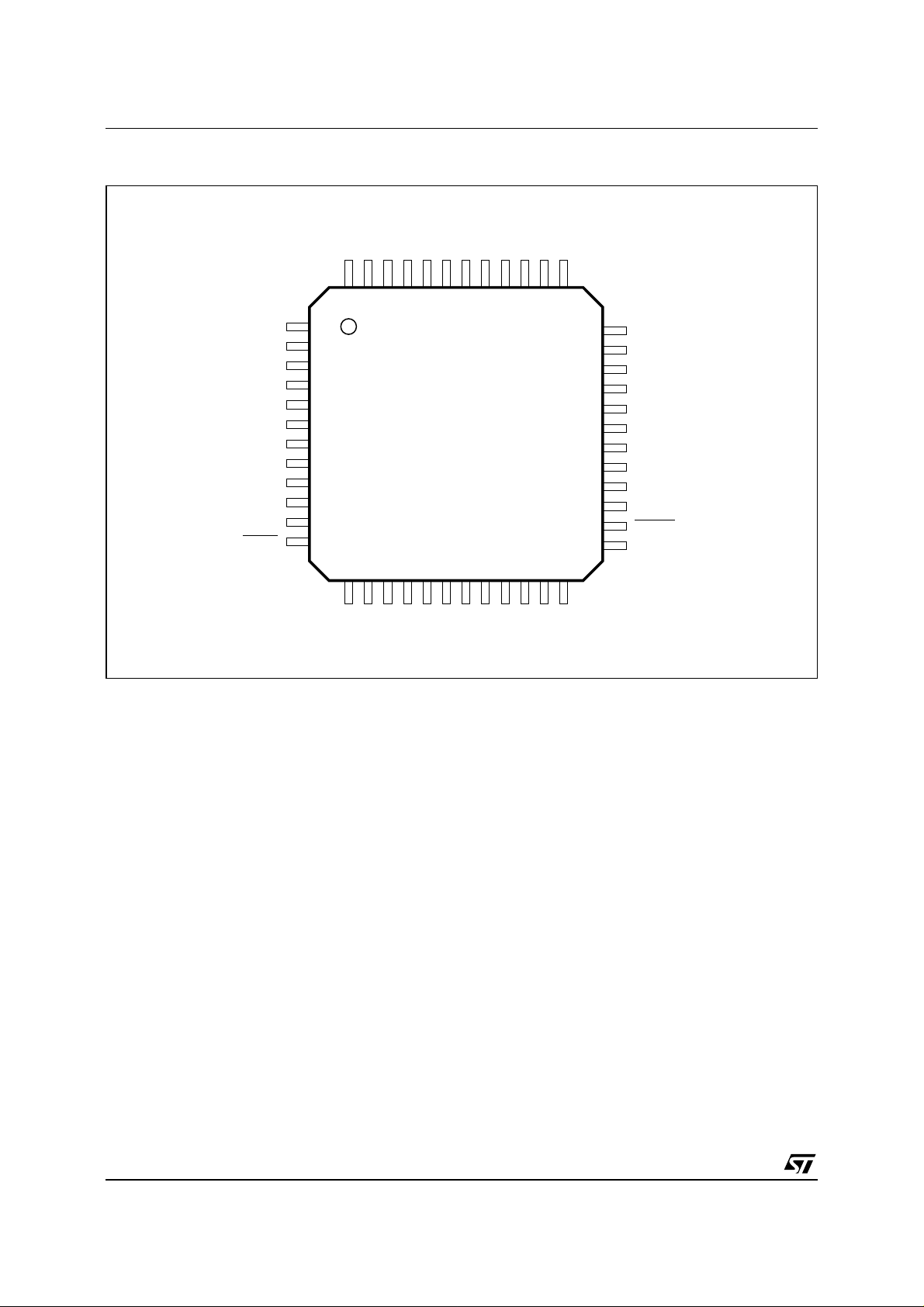
PIN CONNECTIONS
RESERVED
RI
47
48
HSDT
46
RESERVED
HO
44
45
BUZEN
PULSE
LED
41
RFC
40
DISHS
39
37
38
CLID
CD
42
43
D+
GNDBUS
VREGD
VBUS
VREGA
AGND
PSM
XTALIN
XTALOUT
FLTPLL
RESET
D-
1
2
3
4
5
6
7
8
9
10
11
12
15
14
13
RESERVED
RESERVED
RESERVED
16
1718192021
RESERVED
RESERVED
RESERVED
RESERVED
RESERVED
RESERVED
22
23
24
RESERVED
RESERVED
RESERVED
36
35
34
33
32
31
30
29
28
27
26
25
DC
TRxD
DAASEL
RESERVED
DGND
DOUT
DIN
MCLK
FS
HC1
PDOWN
RESERVED
7554S-01.EPS
2/11
Page 3

PIN LIST
Name Pin Type Description
XTALIN 9 I Crystal Input
XTALOUT 10 O Crystal Output
RESET 12 I Reset Function to initialise the device (active low)
VBUS 5 I Positive Voltage Regulator Input, connected to USB VBUS
GNDBUS 3 I Regulator Ground, connected to USB Ground (0V) (see Note 1)
VREGA 6 I/O Positive Regulated Analog Input/Output Power Supply
VREGD 4 I/O Positive Regulated Digital Input/Output Power Supply
PSM 8 I Power Supply Mode (Bus-powered or Self-powered)
D+ 2 I/O Positive Data Signal of Differenti al Data Bus confor ming to USB Standard
D- 1 I/O Negative Data Signal of Differential Data Bus conforming to USB Standard
TRxD 35 I/O Transmit/Receive Data Led
DC 36 I/O DC mask
BUZEN 37 I/O Buzzer Amplifier Enable/Mute
PULSE 38 I/O Pulse dialing
DISHS 39 I/O Disconnect external phone
RFC 40 I/O Refresh
LED 41 I/O LED control
CD 42 I/O Carrier Detect Led
CLID 43 I/O Caller ID
HO 45 I/O Hook Control
HSDT 46 I/O Current sense
RI 48 I/O Ring Indicator
HC1 27 O Modem Codec Hardware Control mode selection
PDOWN 26 O SSI Powerdown bit output (active low)
MCLK 29 O SSI Master Clock Output
DAASEL 34 I Select Silicon or Discrete DAA Configuration Mode
FS 28 I SSI Frame Synchronisation Input
DOUT 31 O SSI Serial Data Output
DIN 30 I SSI Serial Data Input
FLTPLL 11 OA PLL filter analog output. Must be connected to analog ground AGND with
DGND 32 I Digital Ground (0V) (see Note 1)
AGND 7 I Analog Ground (0V) (see Note 1)
RESERVED 13 to 25-33-44 - Not connected
RESERVED 47 - Connect to digital ground DGND
Note 1 :
Analog and digital ground pins must be tied together to USB ground GNDBUS.
Specification 1.0
Specification 1.0
33pF capacitor
ST7554
7554S-01.TBL
3/11
Page 4

ST7554
PIN DESCRIPTION
1 - Power Supply
1.1 - Regulator Input Power Supply
This pin must be connected to USB VBUS (+5V).
It supplies the integrated analog USB transceiver.
It is also the positive regulator power supply input
(5V) when ST7554 is in bus-powered mode
(PSM = 1) and it is used to internally generate the
3.3V supply for the digital and analog circuitry.
1.2 - Regulated Analog V
This pin is the analog power supply input (PSM = 0)
or analog 3.3V power supply output (PSM = 1).
This pin is the positive analog power supply for the
external Codec and DAA.
It is recommended to add a 1µF capacitor between
VREGA and GNDA as close as possible to the
IC pins.
1.3 - Regulated V
This pin is the digital power supply input (PSM = 0)
or digital 3.3V power supply output (PSM = 1).
This pin is the positive digital power supply for the
external Codec and DAA.
It is recommended to add a 1µF capacitor between
VREGA and GNDA as close as possible to the
IC pins.
1.4 - Power Supply Mode
This pin controls the VREGD and VREGA power
supply mode.
When PSM = 1, the application is bus-powered.
The 3.3V power supply is generated internally from
VBUS. In this case VREGD and VREGA are outputs which can be used to supply 3.3V to external
devices (see Figure 1).
When PSM = 0, the application is self-powered.
VBUS must be still connected to the VBUS Pin of
the USB connector in order to supply the integrated
USB transceiver . Anyway in this case VREGD and
VREGA mus t be fed by a 3.3V externally regulated
digital and analog power supplies (see Figure 2).
(7 pins)
Supply
DD
Supply
DD
(VREGD)
(PSM)
(VBUS)
(VREGA)
Figure 1 :
from USB
to other
digital ICs
to other
analog ICs
Figure 2 :
from USB
from 3.3V
externally
regulated
supplies
ST7554 in Bus-Powered mode
(PSM = 1)
ST7554
PSM
8
VBUS
5
GNDBUS
3
VREGD
4
DGND
32
VREGA
6
AGND
7
ST7554 in Self Powered mode
(PSM = 0)
ST7554
PSM
8
VBUS
5
GNDBUS
3
VREGD
4
DGND
32
VREGA
6
AGND
7
7554S-02.EPS
7554S-03.EPS
1.5 - Ground
(DGND, AGND and GNDB US)
DGND, AGND and GNDBUS are the digital, analog
and USB ground return pins respectively.
They should be connected together outside the
chip to the GND pin of the USB plug.
4/11
2 - USB Interface
(D+ , D-)
These pins are the positive and negative USB
differential data lines. They shall be both connected
to the USB plug or USB protection circuit via 27
Ω
series resistors for line impedance matching.
Page 5

ST7554
PIN DESCRIPTION
3 - Reset, Powerdown
(continued)
RESET, PDOW N)
(
RESET Pin initialises the internal counters and
control registers to their default v alue. A minimum
low pulse of 1ms is required to reset the chip.
In a typical application
RESET is connected to
VBUS through a R, C network. This ensures that
the chip is reset at each connection / disconnection
to the USB bus (see Figure 3).
PDOWN Pin shall be connec ted to the powerdown
inputs of the external codec used on the SSI.
When ST7554 is in Suspend mode,
PDOWN i s
forced low so that the external codec is in
powerdown.
VBUS
RESET
12
RESET
Figure 3 :
RC network for
R
220k
W
C
10nF
4 - Serial Synchronous Interface
ST7554 has a Serial Syncronous Interface (SSI)
dedicated to the connection of the STLC7550 or
ST75951, ST high performance Modem Analog
Front-End (MAFE).
4.1 - Data
(DIN, DOUT)
Digital data word input/output of SSI, to be connected to the data word pins of STLC7550 or
ST75951.
4.2 - Master Clock
(MCLK)
This pin is the master clock output.
4.3 - Frame Synchronization
(FS)
The frame sync hronization is used to sy nchronize data
transfer betw een ST75 54 and the ext ernal Co dec.
based on ST75951 + ST952. Connect to DGND
when using STLC7550 with discrete interface.
5 - DAA Con trol Pins
(IMP, DC, BUZEN,
PULSE, DISHS, RFC, LED, CLID, HO, HSDT, RI)
These pins control the World Wide software
programmable DAA through ST759 51/ST952 .
6 - Crystal
(XTA LI N, XTALOUT)
These pins must be tied to the 9.216MHz external
crystal.
It is recommended to use a ±50ppm fundamental
parallel resonator crystal. It is recommended to
insert a 1.8kΩ resistor between XTALOUT and the
crystal to limit its energy to 100µW for a 20
resonator (see Figure 4).
For a SMD crystal the load capacitor is typically
= 12pF and this leads to an ideal value of
C
LOAD
C = 24pF for the capacitors between the crystal
and analog ground (AGND). Anyway, in practice
these capacitors shall be reduced down to
C = 18pF each by considering parasitic capacitors
on PCB and package (see Figure 4).
7554S-04.EPS
After a reset or when leavin g the s uspend state,
the 9.216MHz is asserted inside ST7554 only
3.5ms late r in or der to wait f or it to be sta ble.
Figure 4 :
Application schematic for the
9.216MHz external crystal
XTAL
IN
9 10
C
18pF
AGND AGND
XTAL
OUT
R
1.8k
C
18pF
W
Ω
7554S-05.EPS
4.4 - Hardware Control
(HC1)
HC1 mus t be connec ted to the c orrespondi ng pin of
STLC7 550 or ST75951 , while their HC 0 Pin shal l be
tied to the 3.3V VREGD digital supply. This pin
selects d ata or control mod es for the Modem Co dec.
4.5 - DAA Selection
(DAASEL)
Connect to VREGD when using silicon DA A chipset
7 - PLL Output Filter
(FLTPLL)
This pin must be connected to the analog ground
(AGND) through a 33pF capacitor.
8 - Reserved Pins
(18 pins)
These pins must be left not connected except
Pin 47 which should be connected to the digital
ground DGND.
5/11
Page 6

ST7554
ELECTRICAL SPECI F ICATIONS
Unless otherwise stated, electrical characteristics are specified over the operating range.
Ty pical values are given for V
= +5V , V
BUS
REGA
= 3.3V, V
REGD
= 3.3V , T
amb
= 25°C.
Absolute Maximum Rating
(AGND = DGND = USB GND = 0V, all voltages with respect to 0V)
Symbol Parameter Value Unit
DV
V
V
T
T
P
Warning : Operation beyond these limits may result in permanent damage to the device. Normal operation is not guaranted at these extremes.
Nominal DC Characteristics
Digital Power Supply -0.3, 6.0 V
DD
Input Current per Pin -10, +10 mA
I
I
Output Current per Pin -20, +20 mA
I
O
Analog Input Voltage -0.3, AVDD + 0.3 V
IA
Digital Input Voltage -0.3, DVDD + 0.3 V
ID
Operating Temperature 0, +70 °C
oper
Storage Temperature -55, +150 °C
stg
Maximum Power Dissipation 200 mW
tot
= 0 to 70°C unless otherwise specified)
(T
amb
Symbol Parameter Min. Typ. Max. Unit
POWER SUPPLY AND COMMON MODE VOLTAGE
V
I
VBUS
I
VBUSS
V
REGA
V
REGD
I
VREGA
I
VREGD
P
DIGITAL INTERFACE (except XTALIN, XTALOUT, PSM and
V
V
V
I
LEAK
I
V
C
PSM,
V
I
LEAK
V
Supply Voltage 4 5 5.25 V
BUS
Supply Current TBD mA
Supply Current in Suspend Mode (PSM = 1) TBD µA
Analog regulated Output Power Supply (PSM =1)
Analog regulated Input Power Supply (PSM =0)
Digital regulated Output Power Supply (PSM =1)
Digital regulated Input Power Supply (PSM =0)
3.4-10%
3.3-10%
3.4-10%
3.3-10%
3.4
3.3
3.4
3.3
Analog regulated Output Current (PSM =1)
Analog regulated Input Current (PSM =0) TBD
Digital regulated Output Current (PSM =1)
Digital regulated Input Current (PSM =0)
Low Power Mode (Suspend mode D2, wake-up on ring enabled) TBD mW
DLP
P
Operating Power (SSI in power-down) TBD mW
D
Operating Power (D0 power state) TBD mW
P
D
20
20
RESET) (these inputs have hysteresis)
High Level Input Voltage
IH
V
Low Level Input Voltage
IL
High Level Output Voltage
OH
Low Level Output Voltage
OL
0.8 x V
0.85 x V
REGD
REGD
0.2 x V
Input Leakage Current ± 1 µA
High Level Output Current (0 < VOL < V
I
OL
Low Level Output Current (V
OH
Schmitt Trigger Hysteresis 0.8 V
HYST
Input Capacitance 3 pF
IN
OHMin.
< VOH < V
OLMax.
)
)-2
REGD
RESET (these inputs have hysteresis)
High Level Input Voltage
IH
V
Low Level Input Voltage
IL
0.7 x V
BUS
Input Leakage Current ± 1 µA
Schmitt Trigger Hysteresis 1 1.3 V
HYST
3.4+10%
3.3+10%VV
3.4+10%
3.3+10%VV
40 mA
mA
mA
mA
REGD
0.4
2mA
mA
0.3 x V
BUS
V
V
V
V
V
V
CRYSTAL OSCILLATOR (XTALIN, XTALOUT)
V
High Level Input Voltage
IH
V
Low Level Input Voltage
IL
I
High Level Input Current
IH
I
Low Level Input Current -20
IL
0.8 x V
0.2 x V
REGA
REGA
V
V
20 µA
µA
6/11
Page 7

UNIVERSAL SERIAL BUS INTERFACE
(see Chapter 7 of USB rev 1.0 for complete Electrical Specification)
ST7554
Nominal DC Characteristics
(D+, D-)
Symbol Parameter Min. Typ. Max. Unit
V
DI
V
CM
V
SE
V
OH
V
OL
I
LO
C
IN
(2) Driver Output Resistance (steady state drive) TBD TBD Ω
R
D
Note 2 :
AC Characteristics
Differential Input Sensitivity [(D+) - (D-)] 0.2 V
Differential Common Mode Range 0.8 2.5 V
Single Ended Receiver Threshold 0.8 2 V
High Level Output Static Voltage (RL of 15kΩ to GND)
Low Level Output Static Voltage (RL of 1.5kΩ to 3.6V)
2.8 3.6
0.3
Hi-Z State Data Line Leakage Current (0V < VIN < 3.3V) ±10 µA
Transceiver Capacitance (Pin to GND) 20 pF
Excludes external resistor. In order to comply with USB Specifications 1.0, external series resistors of 27Ω ±1% each on D+ and Dare recommended
(D+, D-) (see Figure 5 for test scheme)
Symbol Parameter Min. Typ. Max. Unit
t
DR
t
R
t
F
V
CRS
Figure 5 :
Average bit rate (12 M/s ± 0.05%) 11.97 12.03 Mbps
Rise Time between 10% and 90% (see Figure 6) 4 20 ns
Fall Time 10% and 90% (see Figure 6) 4 20 ns
Output Signal Crossover Voltage 1.3 2 V
T es t Scheme for D+/D-
V
REGD
Figure 6 :
Rise and Fall Time Measures
V
V
D+
D-
t
W
1.5k
27
W
2
Test
27
W
1
50pF
15k
W
50pF
Test
15k
W
7554S-06.EPS
R
10%
90%
90%
t
10%
F
7554S-07.EPS
7/11
Page 8

ST7554
TYPICAL APPLICATIONS
Figure 7 :
Figure 8 :
ST7554 Typical Application Diagram wit h ST75951/ST952
USB
ST7554 Typical Application Diagram wit h STLC7550
USB
ST75951 ST952ST7554
STLC7550 DAAST7554
POTS
7554S-08.EPS
POTS
7554S-09.EPS
8/11
Page 9

ST7554
TYPICAL APPLICATIONS
Figure 9 :
ST7554 Schematic Diagram with ST75951/ST952
123
USB
Plug
6
7
8
USB6
C26 C27
R18
R17
DD
DV
C15
C14
C30C31
D4
DD
AV
L3
84126
10
R19
5
VBUS
PSM
V
REGD
RESET
V
REGA
FLTPLL
R19
3
214
C29
2
1
D-
D+
LED
41
R16
C11
(continued)
U4
4
5
L4
U5
R20
C28
7
3
32
RI
HO
AGND
DGND
GNDBUS
CLID
DIN
DOUT
RESERVED
RESERVED
IC1
RESERVED
DAASEL
ST7554
HC1
PDOWN
FS
MCLK
XTALIN
XTALOUT
9
10
R14
K1
C13
C12
LED
GND
C24
C22
C16
DD
DV
C25
C17 C23
C18
REF
SET25LCOM32LCOM6TOFF
18
C19
C21
C20
AGND
18 47
17 31 30 43 45 48
34
27
26
28
29
R15
DD
DV
4 44
MCM
GPI
16
9
HC1
PWRDWN
11
3
FS
2
SCLK
8
XTALIN
7
XTALOUT
HM
42
HC0
10
RESET
43
M/S
14
U1
IC3
ST952
DIN
DOUT
D1
D2
35
34
30
31
D1
D2
LINI
LIM124GAIN
8
23
GPIO0
46
TS
U2
GPIO1
D3
31
1
D3
17
GPIO2
GPIO3
IC2
ST75951
D4
30
2
D4
OHC10COM
11
28
RING
TSTA1
D5
27
U3
4
TER19IDC16TER2
17
D5
TSTA2
D6
26
5
D6
5
DV
DD
AUXIN
TSTD1
6
DGND
AV
40
DD
V
21
REFP
G2
V
29
CMP
G1
V
39
CM
V
32
CMS
V
22
REFN
AGND2
38
AGND1
23
C10
26
27
AIN
AOUT
RIN
LINE22IDI
20
IDG19VDR15VDREF14I
21
3
41
45
33
15
18
19
20
47
C5
C3
R0
L1
Details may change without notice.
Refer to ST USB Dongle Modem documentation.
Note : This is an example schematic.
B1
Line
R5
Q1
R2
T1
Plug
Q2
R4
Q3
Q4
R9
R3
C4
R1
L2
Q5
D1
R10C9R11
D2
R6
R12 R7
C6 C7 R8 C8
7554S-10.EPS
9/11
Page 10

ST7554
TYPICAL APPLICATIONS
Figure 10 :
ST7554 Schematic Diagram with STLC7550 (in TQFP48 package)
USB
Plug
USB6
C6 C5
R2
R3
C2 C3
L1
DD
DV
C7
C24
L4
C23C25
DD
AV
(continued)
123
6
7
8
3
214
R6
R7
L2
C13
C12
2
1
5
D-
D+
VBUS
84126
PSM
V
REGD
RESET
ST7554
V
REGA
FLTPLL
10
XTALOUT
LED
10
41
U4
4
5
U1
3
32
DGND
GNDBUS
RESERVED
RESERVED
RESERVED
IC1
XTALIN
RI
9
48
7
DIN
AGND
DOUT
DAASEL
HC1
PDOWN
MCLK
HO
45
L3
GND
DOUT
DIN
44 45
TS
7 42
MCM
TSTD1
43
HC1
15
PWRDWN
17
4
FS
3
SCLK
9
XTALIN
8
XTALOUT
DD
DV
18
M/S
16R541
HC0
IC2
STLC7550
IN+
OUT+
29
C20
RESET
DGND
AUXIN-
AUXIN+
AGND2
AGND1
OUT403039
DD
C19
DV
C18
C15 C8
C14
C10
C16
C11
AGND
5
DV
DD
6
AV
31
DD
V
19
REFP
28
C9
V
CM
27 32
V
C17
20
REFN
33
21
IN-
G1 G2
18 47
17 31 30
34
27
26
FS
28
29
R8
This is an example schematic.
Details may change without notice.
Refer to ST USB Dongle Modem documentation.
Note :
R10
C22
R9
K1
C21
D1
DD
DV
D2 D4
R32
R14
3
6
D5
C27
R1
14
R21
R13
Line
R23
R28
R16
C35
R17
6
5
U3
7
C39
R18
T1
C28
B1
L6
Plug
R29
R33
3
2
U3
CM
V
1
C38
C32
C31
R20
R24
Q1
R22D3
C1
U3
AGND
12
13
R15 C30
R19
R11
4
1
2
7
5
8
T2
L5
R12
R4
8
R26
Q2
C36
9
C37
R25
R31
C4
U3
AGND
10
R27
R30
7554S-11.EPS
10/11
Page 11

PACKAGE MECHANICAL DATA
48 PINS - THIN PLASTIC QUAD FLAT PACK (TQFP)
48 37
1
e
36
ST7554
A
A2
A1
0,10 mm
.004 inch
SEATING PLANE
B
c
Dimensions
E
E3
E1
12
13 24
D3
D1
D
25
L1
L
K
0,25 mm
.010 inch
GAGE PLANE
Millimeters Inches
Min. Typ. Max. Min. Typ. Max.
A 1.60 0.063
A1 0.05 0.15 0.002 0.006
A2 1.35 1.40 1.45 0.053 0.055 0.057
B 0.17 0.22 0.27 0.007 0.009 0.011
C 0.09 0.20 0.004 0.008
D 9.00 0.354
D1 7.00 0.276
D3 5.50 0.216
e 0.50 0.0197
E 9.00 0.354
E1 7.00 0.276
E3 5.50 0.216
L 0.45 0.60 0.75 0.018 0.024 0.030
L1 1.00 0.039
K0
o
(Min.), 7o (Max.)
PM-5B.EPS
5B.TBL
Information furnished is believed to be accurate and reliable. However, STMicroelectronics assumes no responsibility for the
consequences of use of such information nor for any infringement of patents or other rights of third parties which may result from
its use. No licence is granted by implication or otherwise under any patent or patent rights of STMicroelectronics. Specifications
mentioned in this publication are subject to change without notice. This publication supersedes and replaces all information
previously supplied. STMicroelectronics products are not authorized for use as critical components in life support devices or sys tem s
without express written approv al of STMi cr oelec troni cs.
Purchase of I
Rights to use these components in a I
Australia - Brazil - Canada - China - France - Germany - Italy - Japan - Korea - Malaysia - Malta - Mexico - Morocco - The Neth erlands
Singapore - Spain - Sweden - Switzerland - Taiwan - Thailand - United Kingdom - U.S.A.
The ST logo is a registered trademark of STMicroelectronics
© 1999 STMicroelectronics - All Rights Reserved
2
C Components of STMicroelectronics, conveys a license under the Philips I2C Pate n t .
2
the I
C Standard Specifications as defined by Phili ps.
STMicroelectronics GROUP OF COMPANIES
2
C system, is granted provided that the system conforms to
http://www.st.com
11/11
 Loading...