

Page 1

ADJUSTABLE INVERTING NEGATIVE OUTPUT
CURRENT MODE PWM REGULATORS
■ 2.7V TO 11V INPUT TO ADJUSTABLE
NEGATIVE OUTPUT CONVERSION
■ 1W GUARANTEED OUTPUT POWER
(V
>4.5V,T≤70°C)
I
■ 68% TYP. EFFICENCY AT 6V
■ VERY LOW QUIESCENT CURRENT:1.2mA
IN ON MODE, 10µA IN SH UT DOWN MODE
■ SOFT START
■ VERY LOW NOISE OUTPUT
■ 160KHz FIXED FREQUENCY OSCILLATOR
■ MIXED BIPOLAR-CMOS TECHNO LOG Y
DESCRIPTION
The ST755 is an adjustable inverting switch-mode
DC-DC regulator with internal Power MOSFET
that generators an adjustable negative output
from a voltage input of 2.7V to 11V , output current
guaranteed at 200mA (for V
>4.5V,VO=-5Vand
I
ST755
DIP-8 SO-8
T
= 0°C to 70°C) and 275mA (typical value at T
A
=25°C,VO=-5V).
A logic controlled shut down pin that interfaces
directly with microprocessor reduces supply
current to only 10mA. Input to Output differential
voltage is limited to V
supply current is 1. 2mA.
+|VO|<12.7V. No load
I
A
SCHEMATIC DIAGRAM
1/10June 2003
Page 2
ST755
ABSOLUTE MAXIMUM RATINGS
Symbol Parameter² Value Unit
V
V
SHDN
V
V
I
LX
P
TOT
T
T
Absolute Maximum Ratings are those values beyond which damage to the device may occur. Functional operation under these condition is
not implied.
Note 1: The input to output differential voltage is limited to V
THERMAL DATA
Symbol Parameter SO-8 DIP-8 Unit
R
thj-amb
(*) This value depends from thermal design of PCB on which the device is mounted.
DC Input Voltage to GND (Note1)
CC
-0.3 to 12 V
Shutdown Voltage, SS Voltage, CC Voltage -0.3 to (VCC+ 0.3)
Switch Voltage (LX to VCC)
LX
Feedback Voltage (VOto GND)
FB
Peak Switch Current
Continuous Power Dissipation at TA= 70°C (DIP-8)
(SO-8)
Operating Junction Temperature Range (C series) -40 to 185 °C
op
Storage Temperature Range
stg
+|VO|<12.7V
CC
Thermal Resistance Junction-ambient (*)
-12.5 to + 0.3 V
-11 to + 0.9 V
2A
725
470
-55 to +150 °C
160 100 °C/W
V
mW
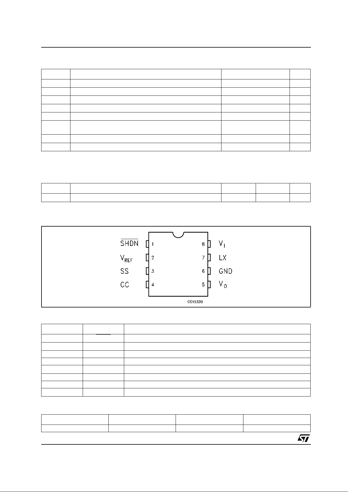
CONNECTION DIAGRAM (top view)
PIN DESCRIPTION
Pin N° Symbol Name and Function
1 SHDN
2V
REF
3 SS Soft Start
4 CC Compensation Input
5V
O
6 GND Ground
7 LX Switch Output
8V
CC
SHUT-DOWN control (VCC= ON, GND = Shutdown)
Reference Output Voltage: (1.25V)
Negative Output Voltage
Supply Voltage Input.
ORDERING CODES
TYPE DIP8 SO-8 SO-8 (T&R)
ST755 ST755CN ST755CD ST755CD-TR
2/10
Page 3
ST755
ELECTRICAL CHARACTERISTICS (Refer to the test circuits , VCC=5V,VO= -5.25 to -4.75V,
I
=0mA,TA=T
LOAD
Symbol Parameter Test Conditions Min. Typ. Max. Unit
VIInput Voltage 4 11 V
Output Voltage VCC= 4.5 to 6.2V IO=0 to 200mA 4.75 5 5.25 V
V
O
Output Current VCC= 4.5 to 6.2V TA= 0 to 70°C 200 275 mA
I
O
I
SUPPLY
I
∆V
∆V
V
∆V
R
I
LEAK
f
Supply Current (Including
Switching Current)
Standby Current) No Load V
OFF
Short Circuit Current) 1.2 A
I
SC
Line Regulation VCC= 4 to 6.2V 0.1 %/V
O
Load Regulation IO= 0 to 200mA 0.003 %/mA
O
Reference Voltage TA= 25°C 1.18 1.25 1.32 V
REF
Reference Drift TA=T
REF
LX On Resistance 0.7 Ω
DSON
LX Leakage Current) VDS= 10V 1 µA
Shutdown Pin Current) 1 µA
I
SH
SHDN Input High Threshold 2 V
V
IH
SHDN Input Low Threshold 0.25 V
V
IL
Oscillator Frequency 160 KHz
OSC
η Power Efficiency I
CC Compensation Pin
Impedance
Do not overload or short the Output to Ground. If the above conditions are observed, the device may be damaged.
MIN
to T
, unless otherwise s pec ified. Typical value are referred at TA= 25°C)
MAX
= 4.5 to 6.2V TA= -40 to 85°C 175
V
CC
=4V VO= -5V 175
V
CC
V
= 2.7V VO= -5V 125
CC
No Load V
to T
MIN
=100mA 68 %
O
MAX
SHDN=VCC
=0V 10 100 µA
SHDN
1.2 3.5 mA
50 ppm/°C
7.5 KΩ
APPLICATION INFORMATION
The ST755 is a n IC developed for voltage conversion from an input volt age ranging from +2.4V to 11V to
a regulated adjustable negative output limite d by |V
| ≤ 12 .7V-VI. The circuit adopts a current-mode PWM
O
control scheme to achieve good efficiency, high stability and low noise performance. The figure in the first
page shown the detailed b lock diagram of the device.
ST755 is realized in a BCD technology in order to achieve high temperature stability, the best
REFERENCE precision, a very low quiescent current and jitter free operat ions. The f inal stage is built
around a 0.7Ω - 2 A P-Channel Power MOS. A f raction of the output curren t is splitted o ut for current
detection.Internal clock frequency is fixed to 160KHz. Error amplifier drives the PWM comparator in order
to keep 0V on the CC input. So R
V
)*R3(see fig 1). For R3can be choose any value between 2KΩ and 20KΩ. Soft-Start (SS) input is a
REF
and R4resistors are calculated by t he following formulae R4= (|VO|/
3
voltage dependent-output current limit (see figure 9, Switch Current Limit vs. SS Input V oltage). SS pin is
internally pulled to V
through a 1.2 MΩ resistor. Applying an appropriate capacitor at SS input is
REF
possible to obtain a s of t-start current imitation during power up. F orcing Soft -Start (SS) input to a lower
voltage through a resistive voltage driver (R
and R2), the maximum LX current limit can be lowered
1
according the diagram showed in figure 9. When SHDN input is l ow, the total current c ons umption is
reduced to 10µA.
APPLICATION CIRCUIT
To achieve the best performances from switch ing power supply topology, particular care to layout drawing
is needed, in order to minimize EMI and obtain low noise, jitter free operati on moreover, it ensures the full
device functionality. Layou t design proposed on demoboard (see pict ure 2) helps to lower the developing
3/10
Page 4

ST755
time. Wire lengths must be minimized, filter and by-pass capacitors C1,C2and C3must be low ESR type,
placed as close possible to the integrated circuit. The 10µH inductor m us t be chosen built on a core,
taking care that saturation c urrent should be higher than t he peak LX switch current. See the PEAK
INDUCTOR CURRENT vs. LOAD CURRENT graph (figure 6 ).
Figure1 : TYPICAL APPLICATION CIRCUIT
(*) R1 and R2 can be omitted for Iout<200mA.
(**) C6: Very low noise but poor transient and load response speed.
(***) C3 (alternative to C6): faster transient and load response.
Figure2 : PRINTED DEMOBOARD
PIN 1 = V
PIN 2 = V
PIN 3 = SHDN
PIN 4 = GND
Note: Drawings not in scale
CC
O
Component Valu es
Capacitor Value Unit Resistor Value Unit
C1 47 µF R1 130 KΩ
C2 100 µF R2 300 KΩ
C3 82 pF R3 10 KΩ
C4 1 µF R4 40.7 KΩ
C5 10 µF R5 10 KΩ
C6 47 pF
4/10
Page 5

TYPICAL PERFORMANCE CHARACTE RISTICS (unless otherwise specified Tj=25°C
ST755
Figure3 : Load Current vs Supply Voltage
Figure4 : Load Current vs Supply Voltage
Figure6 : Peak Inductor Current vs Load Current
Figure7 : Switch ON Resistance vs Supply
Voltage
Figure5 : Efficiency vs Load Current
Figure8:Oscillator Frequenc y vs T emperature &
Supply Voltage
5/10
Page 6

ST755
Figure9 : Switch Current Limit vs Soft Start
Voltage
Figure10 : Refe renc e Voltage Vs Temperature
Figure11 : Soft Start Delay Time
6/10
Page 7

Plastic DIP-8 MECHANICAL DATA
ST755
DIM.
MIN. TYP MAX. MIN. TYP. MAX.
A 3.3 0.130
a1 0.7 0.028
B 1.39 1.65 0.055 0.065
B1 0.91 1.04 0.036 0.041
b 0.5 0.020
b1 0.38 0.5 0.015 0.020
D 9.8 0.386
E 8.8 0.346
e 2.54 0.100
e3 7.62 0.300
e4 7.62 0.300
F 7.1 0.280
I 4.8 0.189
L 3.3 0.130
Z 0.44 1.6 0.017 0.063
mm. inch
P001F
7/10
Page 8

ST755
SO-8 MECHANICAL DATA
DIM.
A 1.35 1.75 0.053 0.069
A1 0.10 0.25 0.04 0.010
A2 1.10 1.65 0.043 0.065
B 0.33 0.51 0.013 0.020
C 0.19 0.25 0.007 0.010
D 4.80 5.00 0.189 0.197
E 3.80 4.00 0.150 0.157
e 1.27 0.050
H 5.80 6.20 0.228 0.244
h 0.25 0.50 0.010 0.020
L 0.40 1.27 0.016 0.050
k ˚ (max.)
ddd 0.1 0.04
MIN. TYP MAX. MIN. TYP. MAX.
mm. inch
8
8/10
0016023/C
Page 9

Tape & Reel SO-8 MECHANICAL DATA
mm. inch
DIM.
MIN. TYP MAX. MIN. TYP. MAX.
A 330 12.992
C 12.8 13.2 0.504 0.519
D 20.2 0.795
N 60 2.362
T 22.4 0.882
Ao 8.1 8.5 0.319 0.335
Bo 5.5 5.9 0.216 0.232
Ko 2.1 2.3 0.082 0.090
Po 3.9 4.1 0.153 0.161
P 7.9 8.1 0.311 0.319
ST755
9/10
Page 10

ST755
Information furnished is believed to be accurate and reliable. However, STMicroelectronics assumes no responsibility for the
consequences of use o f suc h inf ormat ion n or f or an y infr ingeme nt of paten ts or oth er ri gh ts of third part ies whic h may resul t f rom
its use. No license is granted by implication or otherwise under any patent or patent rights of STMicroelectronics. Specifications
mentioned in this publication are subject to change without notice. This publication supersedes and replaces all information
previously supplied. STMicroelectronics products are not authorized for use as critical components in life support devices or
systems without express written approval of STMicroelectronics.
Australia - Brazil - Canada - China - Finland - France - Germany - Hong Kong - India - Israel - Italy - Japan - Malaysia - Malta - Morocco
© The ST logo is a registered trademark of STMicroelectronics
© 2003 STMicroelectronics - Printed in Italy - All Rights Reserved
STMicroelectronics GROUP OF COMPANIES
Singapore - Spain - Sweden - Switzerland - United Kingdom - United States.
© http://www.st.com
10/10
 Loading...